EP1753162A1 - Synchronization of data streams from data acquisition processors using a shared signal - Google Patents
Synchronization of data streams from data acquisition processors using a shared signal Download PDFInfo
- Publication number
- EP1753162A1 EP1753162A1 EP06254134A EP06254134A EP1753162A1 EP 1753162 A1 EP1753162 A1 EP 1753162A1 EP 06254134 A EP06254134 A EP 06254134A EP 06254134 A EP06254134 A EP 06254134A EP 1753162 A1 EP1753162 A1 EP 1753162A1
- Authority
- EP
- European Patent Office
- Prior art keywords
- data acquisition
- data
- processors
- signal
- phase
- Prior art date
- Legal status (The legal status is an assumption and is not a legal conclusion. Google has not performed a legal analysis and makes no representation as to the accuracy of the status listed.)
- Withdrawn
Links
Images


Classifications
-
- G—PHYSICS
- G06—COMPUTING OR CALCULATING; COUNTING
- G06F—ELECTRIC DIGITAL DATA PROCESSING
- G06F1/00—Details not covered by groups G06F3/00 - G06F13/00 and G06F21/00
- G06F1/04—Generating or distributing clock signals or signals derived directly therefrom
- G06F1/12—Synchronisation of different clock signals provided by a plurality of clock generators
-
- H—ELECTRICITY
- H04—ELECTRIC COMMUNICATION TECHNIQUE
- H04J—MULTIPLEX COMMUNICATION
- H04J3/00—Time-division multiplex systems
- H04J3/02—Details
- H04J3/06—Synchronising arrangements
- H04J3/0635—Clock or time synchronisation in a network
- H04J3/0682—Clock or time synchronisation in a network by delay compensation, e.g. by compensation of propagation delay or variations thereof, by ranging
Definitions
- the invention relates to the field of data processing and display. More particularly, the invention relates to the field of synchronizing processed data streams.
- a PLL includes a voltage- or current-driving oscillator that is constantly adjusted to match in phase (and thus lock onto) the frequency of an input signal.
- a PLL can be used to generate a signal, modulate or demodulate a signal, reconstitute a signal with less noise, or multiply or divide a frequency.
- Fig. 1 illustrates the classic PLL 10 configuration.
- the phase detector 15 is a device that compares input frequencies 35, 40, generating a phase error signal 50 that is a measure of their phase difference (if, for example, the input frequencies 35, 40 differ in frequency, it gives a periodic output at the difference frequency). If f IN 35 doesn't equal f VCO 40, the phase-error signal 50, after being filtered in the loop filter 20 and amplified in the voltage controlled oscillator (VCO) 25, causes the f VCO 40 frequency to deviate in the direction of f IN 35. If conditions are right, the f VCO 40 will quickly "lock" to f IN 35 maintaining a fixed relationship with the input signal 35.
- VCO voltage controlled oscillator
- the filtered output frequency (Fout) 40 of the phase detector 25 is a dc signal, and the control input to the VCO 25 is a measure of the input frequency 35, with obvious applications to tone decoding (used in digital transmission over telephone lines) and FM detection.
- the VCO 25 output Fout 40 is a locally generated frequency equal to f IN 35, thus providing a clean replica of f IN 35, which may itself be noisy. Since the VCO 25 output Fout 40 can be a triangle wave, sine wave, or any other type of wave, this provides a nice method of generating a sine wave locked to a train of pulses.
- a modulo-n counter 30 is hooked between the VCO 25 output Fout 40 and the phase detector 15, thus generating a multiple of the input reference frequency f IN 35.
- This is an ideal method for generating clocking pulses at a multiple of the power-line frequency for integrating A/D converters (dual-slope, charge-balancing), in order to have infinite rejection of interference at the power-line frequency and its harmonics. It also provides the basic technique of frequency synthesizers.
- Various aspects and embodiments of the present invention relate to a system and method of synchronizing data streams from data acquisition processors.
- the system and method utilizes a common signal to data acquisition processors to trigger a measuring of the data sampling signal. These measurements are averaged and compared to an expected phase, whereby either of the data acquisition processor's data delivery rate are adjusted if the compound shows a difference greater than a maximum drift rate.
- Various aspects and embodiments of the present invention include a method of synchronizing a set of data streams, which comprises routing a common signal to a first data acquisition processor and a second data acquisition processor, wherein the common signal triggers the first and second data acquisition processors to take a plurality of phase measurements of a sampling signal, averaging the plurality of phase measurements, comparing the averaged phase measurements of each of the first and second data acquisition processors to an expected phase, and adjusting a digital control signal of either one of the first and second data acquisition processors when the difference between the average phase measurement of either data acquisition processor and the expected phase exceeds a maximum drift rate, wherein the common signal is generated by an administrative processor.
- Various aspects and embodiments of the present invention include a system for synchronizing a set of data streams, which comprises a first data acquisition processor and a second data acquisition processor, the first and second data acquisition processors configured to receive a common signal, and an administrative processor configured to receive a data signal from each of the data acquisition processors and to generate the common signal, wherein the first and second data acquisition processors take a plurality of phase measurements of a sampling signal and average the phase measurements when the common signal is received, and further wherein the first and second data acquisition processors compare the average phase measurements to an expected phase, such that a digital control signal of either one of the first and second data acquisition processors is adjusted when the difference between the average phase measurements and the expected phase exceeds a maximum drift rate.
- Various aspects and embodiments of the present invention include a method of synchronizing a set of data streams, which comprises generating a common signal with an administrative processor, routing the common signal to a first data acquisition processor and a second data acquisition processor, wherein the common signal triggers the first and second data acquisition processors to take a plurality of phase measurements of a sampling signal, averaging the plurality of phase measurements, comparing the averaged phase measurements of each of the first and second data acquisition processors to an expected phase, and adjusting a digital control signal of either one of the first and second data acquisition processors when the difference between the average phase measurement of either data acquisition processor and the expected phase exceeds a maximum drift rate.
- a common signal 180 is routed to a set of data acquisition processors 120, 135. It should be understood that embodiments of the invention may include more than two data acquisition processors 120, 135 and that Figure 2 depicts the preferred embodiment including two data acquisition processors 120, 135.
- the common signal 180 is used by each data acquisition processor 120, 135 to trigger a measurement of the phase of the signal used in its data sampling. These phase measurements are averaged across a number of iterations, and then compared to an expected phase value. If the difference between the measured and expected phase exceeds a maximum drift rate, an adjustment is made to the data acquisition processor's 120, 135 data delivery rate to compensate.
- each data acquisition processor's 120, 135 data delivery rate may drift back or forth, but will be centered around a rate dictated by the common signal input, resulting in an effective synchronization of the data signals 175 from the data acquisition processors 120, 135.
- the data delivery rate of each data acquisition processor 120, 135 is a function of the rate at which it samples data.
- this sample rate is performed using on-chip timers, set to sample the data at a predefined period. Specifically, the timers will repeatedly count from 0 to a predefined value, with a new sample collected at each timer restart. Synchronization will be implemented by adjusting this mechanism directly, either by moving the timer count ahead or behind, depending on the direction of the synchronization required. The effect is that the sampling is adjusted in phase, and aligned with that of the common signal. This will occur each time phase misalignment between the data acquisition processors 120, 135 sampling timers and the common signal exceeds the adjustment threshold.
- An additional component of this embodiment of the invention is enhanced noise-immunity.
- the common signal 180 provided to each data acquisition processor 120, 135 will be uncorrupted. However, synchronization will still occur under noisy conditions, and with the resulting, associated corrupted common signal 180 arriving at the processors. This is done by monitoring for, and rejecting, "outlier" samples that occur under these conditions, and that exceed the known range of valid readings. Rejected samples will be replaced with the last valid sample, for designated duration of continuously occurring noise and corrupted signal.
- phase compensation is performed on each data acquisition processor 120, 135 separately, resulting in the data streams 175 from both being synchronized to the common signal 180, and to each other. Without such a common signal, data delivered 175 from the data acquisition processors 120, 135 would drift apart, making diagnosis derived from comparison of the associated data sets difficult and inaccurate. Other cruder methods of compensating for this drift are possible, like dropping a sample from the data streams every so often. But these types of approaches result in large data discontinuities at the point of adjustment, and significant amounts of drift before it is applied. Complex, downstream adjustments to the data are also required, whereas the present invention performs the compensation at the optimal, earliest stage of its collection.
- a novel approach to noise immunity is provided by this invention as well, by allowing synchronization of the data acquisition processors 120, 135 in the presence of noise. It will overcome reasonable and expected levels of noise corruption, by rejecting and compensating for "outlying" samples of the common signal, and without negative effect on the overall synchronization.
- the signal 210 represents the common signal produced by the administrative processor 105 ( Figure 2), and utilized by the data acquisition processors 120, 135 to synchronize the data signals 175.
- the digital control signal 160 instructs the A/D 150 at what rate to sample the analog signal, and the resultant digital signal 165 is sent to the data acquisition processors 120, 135.
- the signal 220 is a representation of a normal timer count, in other words, a timer count 220 that would ordinarily be used by a data acquisition processor 120, 135.
- the adjusted timer count signals 230 show an adjusted saw tooth 235, as would be implemented in the present invention when the drift exceeds a predetermined level.
- the adjusted saw tooth 235 of the adjusted timer count signal 230 represents the timer of the data acquisition processor 120, 135 being adjusted up or down when the drift exceeds a predetermined level.
- the adjusted digital control signal 160 to the A/D 150, 155 will result in synchronizing the data delivery rate.
- the synchronizing method 300 of the present invention is further depicted in Figure 4.
- a common signal is routed to a first data acquisition processor and a second data acquisition processor.
- a plurality of phase measurements of a sampling signal are taken by the data acquisition processors.
- the plurality of phase measurements taken in the data acquisition processors are averaged, and the averages are compared in step 320 to an expected phase. If the averages exceed the expected phase by a predetermined amount, in step 325 the digital control signals are adjusted, such that the sampling rates are modified, resulting in synchronized data delivery in step 325.
Landscapes
- Engineering & Computer Science (AREA)
- Theoretical Computer Science (AREA)
- Physics & Mathematics (AREA)
- General Engineering & Computer Science (AREA)
- General Physics & Mathematics (AREA)
- Computer Networks & Wireless Communication (AREA)
- Signal Processing (AREA)
- Stabilization Of Oscillater, Synchronisation, Frequency Synthesizers (AREA)
- Synchronisation In Digital Transmission Systems (AREA)
Abstract
Description
- The invention relates to the field of data processing and display. More particularly, the invention relates to the field of synchronizing processed data streams.
- When data acquisition processors are used to generate data consumed by an administrative processor, the data sets coming from the data acquisition processors need to be time aligned, even though they are generated from separate processors, each having their own CPU clock. Without correction, the data sets would drift apart from each other, because the crystals used to generate the CPU clock for each processor are not exactly the same frequency.
- Current solutions of compensating for this drift include dropping a sample from one of the data streams every so often. However, this type of approach results in large data discontinuities at the point of adjustment, and significant amounts of drift before it is applied. Complex, downstream adjustments to the data are also required.
- In understanding the present invention, it will be beneficial to note that a PLL includes a voltage- or current-driving oscillator that is constantly adjusted to match in phase (and thus lock onto) the frequency of an input signal. In addition to stabilizing a particular communications channel (keeping it set to a particular frequency), a PLL can be used to generate a signal, modulate or demodulate a signal, reconstitute a signal with less noise, or multiply or divide a frequency.
- Fig. 1 illustrates the
classic PLL 10 configuration. Thephase detector 15 is a device that comparesinput frequencies phase error signal 50 that is a measure of their phase difference (if, for example, theinput frequencies f IN 35 doesn't equalf VCO 40, the phase-error signal 50, after being filtered in theloop filter 20 and amplified in the voltage controlled oscillator (VCO) 25, causes thef VCO 40 frequency to deviate in the direction off IN 35. If conditions are right, thef VCO 40 will quickly "lock" tof IN 35 maintaining a fixed relationship with theinput signal 35. At that point, the filtered output frequency (Fout) 40 of thephase detector 25 is a dc signal, and the control input to theVCO 25 is a measure of theinput frequency 35, with obvious applications to tone decoding (used in digital transmission over telephone lines) and FM detection. The VCO 25output Fout 40 is a locally generated frequency equal tof IN 35, thus providing a clean replica off IN 35, which may itself be noisy. Since theVCO 25output Fout 40 can be a triangle wave, sine wave, or any other type of wave, this provides a nice method of generating a sine wave locked to a train of pulses. - In one of the most common applications of
PLLs 10, a modulo-n counter 30 is hooked between theVCO 25output Fout 40 and thephase detector 15, thus generating a multiple of the inputreference frequency f IN 35. This is an ideal method for generating clocking pulses at a multiple of the power-line frequency for integrating A/D converters (dual-slope, charge-balancing), in order to have infinite rejection of interference at the power-line frequency and its harmonics. It also provides the basic technique of frequency synthesizers. - Various aspects and embodiments of this invention make use of the design principles behind
PLLs 10, which is considered prior art. However,PLL 10 principles and techniques are applied in a novel way. - Various aspects and embodiments of the present invention relate to a system and method of synchronizing data streams from data acquisition processors. The system and method utilizes a common signal to data acquisition processors to trigger a measuring of the data sampling signal. These measurements are averaged and compared to an expected phase, whereby either of the data acquisition processor's data delivery rate are adjusted if the compound shows a difference greater than a maximum drift rate.
- Various aspects and embodiments of the present invention include a method of synchronizing a set of data streams, which comprises routing a common signal to a first data acquisition processor and a second data acquisition processor, wherein the common signal triggers the first and second data acquisition processors to take a plurality of phase measurements of a sampling signal, averaging the plurality of phase measurements, comparing the averaged phase measurements of each of the first and second data acquisition processors to an expected phase, and adjusting a digital control signal of either one of the first and second data acquisition processors when the difference between the average phase measurement of either data acquisition processor and the expected phase exceeds a maximum drift rate, wherein the common signal is generated by an administrative processor.
- Various aspects and embodiments of the present invention include a system for synchronizing a set of data streams, which comprises a first data acquisition processor and a second data acquisition processor, the first and second data acquisition processors configured to receive a common signal, and an administrative processor configured to receive a data signal from each of the data acquisition processors and to generate the common signal, wherein the first and second data acquisition processors take a plurality of phase measurements of a sampling signal and average the phase measurements when the common signal is received, and further wherein the first and second data acquisition processors compare the average phase measurements to an expected phase, such that a digital control signal of either one of the first and second data acquisition processors is adjusted when the difference between the average phase measurements and the expected phase exceeds a maximum drift rate.
- Various aspects and embodiments of the present invention include a method of synchronizing a set of data streams, which comprises generating a common signal with an administrative processor, routing the common signal to a first data acquisition processor and a second data acquisition processor, wherein the common signal triggers the first and second data acquisition processors to take a plurality of phase measurements of a sampling signal, averaging the plurality of phase measurements, comparing the averaged phase measurements of each of the first and second data acquisition processors to an expected phase, and adjusting a digital control signal of either one of the first and second data acquisition processors when the difference between the average phase measurement of either data acquisition processor and the expected phase exceeds a maximum drift rate.
- Various aspects and embodiments of the present invention will now be described in connection with the accompanying drawings, in which:
- Figure 1 is a block diagram illustrating a Phase Locked Loop (PLL) circuit.
- Figure 2 is a block diagram illustrating a system according to an embodiment of the present invention.
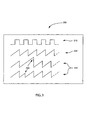
- Figure 3 is a graphical representation illustrating waveforms according to an embodiment of the present invention.
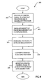
- Figure 4 is a flow chart illustrating a method according to an embodiment of the present invention.
- As shown in Figure 2, a
common signal 180 is routed to a set ofdata acquisition processors data acquisition processors data acquisition processors common signal 180 is used by eachdata acquisition processor data acquisition processors - The data delivery rate of each
data acquisition processor data acquisition processor data acquisition processors - An additional component of this embodiment of the invention is enhanced noise-immunity. Under normal circumstances, the
common signal 180 provided to eachdata acquisition processor common signal 180 arriving at the processors. This is done by monitoring for, and rejecting, "outlier" samples that occur under these conditions, and that exceed the known range of valid readings. Rejected samples will be replaced with the last valid sample, for designated duration of continuously occurring noise and corrupted signal. - In the medical field, various embodiments of this invention will result in more accurate data presentation to medical personnel, with a likely associated increase in customer satisfaction, and enhanced marketing appeal. The most common method of synchronizing data streams from multiple processors is for them to use a shared CPU clock. However, this embodiment of the present invention was designed in a system that would not easily allow for this type of approach, primarily as a result of a requirement that the
data acquisition processors common signal 180 of this invention, and use it to adjust the phase of the sampling on thedata acquisition processors data acquisition processor common signal 180, and to each other. Without such a common signal, data delivered 175 from thedata acquisition processors data acquisition processors - Referring now to Figure 3, a
signal profile 200 of the signals discussed previously in accordance with the present invention is depicted. Thesignal 210 represents the common signal produced by the administrative processor 105 (Figure 2), and utilized by thedata acquisition processors data signals 175. Thedigital control signal 160 instructs the A/D 150 at what rate to sample the analog signal, and the resultantdigital signal 165 is sent to thedata acquisition processors signal 220 is a representation of a normal timer count, in other words, atimer count 220 that would ordinarily be used by adata acquisition processor timer count signals 230 show an adjustedsaw tooth 235, as would be implemented in the present invention when the drift exceeds a predetermined level. Here, the adjustedsaw tooth 235 of the adjustedtimer count signal 230 represents the timer of thedata acquisition processor digital control signal 160 to the A/D - The
synchronizing method 300 of the present invention is further depicted in Figure 4. Instep 305, a common signal is routed to a first data acquisition processor and a second data acquisition processor. Instep 310, a plurality of phase measurements of a sampling signal are taken by the data acquisition processors. Instep 315, the plurality of phase measurements taken in the data acquisition processors are averaged, and the averages are compared instep 320 to an expected phase. If the averages exceed the expected phase by a predetermined amount, instep 325 the digital control signals are adjusted, such that the sampling rates are modified, resulting in synchronized data delivery instep 325. - The present invention has been described in terms of specific embodiments incorporating details to facilitate the understanding of the principles of construction and operation of the invention. Such reference herein to specific embodiments and details thereof is not intended to limit the scope of the claims appended hereto. It will be apparent to those skilled in the art that modifications may be made in the embodiment chosen for illustration without departing from the spirit and scope of the invention.
-
Component Part Reference Number Figure Number Phase Lock Loop 10 Figure 1 Phase Detector 15 Figure 1 Loop Filter 20 Figure 1 Voltage Controlled Oscillator (VCO) 25 Figure 1 N Counter 30 Figure 1 Input Frequency (Fin) 35 Figure 1 Output Frequency (Fout) 40 Figure 1 VCO Frequency (Fvco) 45 Figure 1 Phase Error Signal 50 Figure 1 Synchronizing System 100 Figure 2 Administrative Processor 105 Figure 2 Data Acquisition Processor 120 Figure 2 Data Acquisition Processor 135 Figure 2 Common Signal Input 2 140 Figure 2 Sample Output 2 145 Figure 2 A/D 1 150 Figure 2 A/D 2 155 Figure 2 Synchronized Analog Signal 160 Figure 2 Synchronized Digital Signal 165 Figure 2 Signal Profile 200 Figure 3 Common Signal 210 Figure 3 Normal Timer Count 220 Figure 3 Adjusted Timer Count 230 Figure 3 Adjusted Sawtooth 235 Figure 3 Synchronizing Method 300 Figure 4 Step 305 Figure 4 Step 310 Figure 4 Step 315 Figure 4 Step 320 Figure 4 Step 325 Figure 4 Data Signal 175 Figure 2 Common Signal 180 Figure 2
Claims (4)
- A method of synchronizing a set of data streams, the method comprising:a. routing (305) a common signal to a first data acquisition (120) processor and a second data acquisition processor (135), wherein the common signal triggers the first and second data acquisition processors (120,135) to take a plurality of phase measurements (310) of a sampling signal;b. averaging (315) the plurality of phase measurements;c. comparing (320) the averaged phase measurements of each of the first and second data acquisition processors (120, 135) to an expected phase; andd. adjusting (325) a digital control signal of either one of the first and second data acquisition processors (120, 135) when the difference between the average phase measurement of either data acquisition processor (120, 135) and the expected phase exceeds a maximum drift rate.
- The method according to claim 1, wherein the common signal is generated by an administrative processor (105).
- A system for synchronizing a set of data streams, the system comprising:a. a first data acquisition processor (120) and a second data acquisition processor (135), the first and second data acquisition processors (120, 135) configured to receive a common signal; andb. an administrative processor (105) configured to receive a data signal from each of the data acquisition processors (120, 135) and to generate the common signal,wherein the first and second data acquisition processors (120, 135) take a plurality of phase measurements of a sampling signal and average the phase measurements when the common signal is received, and further wherein the first and second data acquisition processors (120, 135) compare the average phase measurements to an expected phase, such that a digital control signal of either one of the first and second data acquisition processors is adjusted when the difference between the average phase measurements and the expected phase exceeds a maximum drift rate.
- A method of synchronizing a set of data streams, the method comprising:a. generating a common signal with an administrative processor (105);b. routing (305) the common signal to a first data acquisition processor (120) and a second data acquisition processor, wherein the common signal triggers the first and second data acquisition processors (120, 135) to take a plurality of phase measurements (310) of a sampling signal;c. averaging (315) the plurality of phase measurements;d. comparing (320) the averaged phase measurements of each of the first and second data acquisition processors (120, 135) to an expected phase; ande. adjusting (325) a digital control signal of either one of the first and second data acquisition processors (120, 135) when the difference between the average phase measurement of either data acquisition processor (120, 135) and the expected phase exceeds a maximum drift rate.
Applications Claiming Priority (1)
| Application Number | Priority Date | Filing Date | Title |
|---|---|---|---|
| US11/199,859 US20070036255A1 (en) | 2005-08-09 | 2005-08-09 | Synchronization of data streams from data acquisition processors using a common signal |
Publications (1)
| Publication Number | Publication Date |
|---|---|
| EP1753162A1 true EP1753162A1 (en) | 2007-02-14 |
Family
ID=37075237
Family Applications (1)
| Application Number | Title | Priority Date | Filing Date |
|---|---|---|---|
| EP06254134A Withdrawn EP1753162A1 (en) | 2005-08-09 | 2006-08-07 | Synchronization of data streams from data acquisition processors using a shared signal |
Country Status (3)
| Country | Link |
|---|---|
| US (1) | US20070036255A1 (en) |
| EP (1) | EP1753162A1 (en) |
| JP (1) | JP2007049705A (en) |
Citations (1)
| Publication number | Priority date | Publication date | Assignee | Title |
|---|---|---|---|---|
| FR2832523A1 (en) * | 2001-11-16 | 2003-05-23 | Alstom | Method for compensating data propagation time differences in distributed system, e.g. for static converter control, comprising phases of module calibration to determine synchronization times and delaying module executions accordingly |
Family Cites Families (11)
| Publication number | Priority date | Publication date | Assignee | Title |
|---|---|---|---|---|
| US6269317B1 (en) * | 1997-04-30 | 2001-07-31 | Lecroy Corporation | Self-calibration of an oscilloscope using a square-wave test signal |
| US5921938A (en) * | 1997-10-09 | 1999-07-13 | Physio-Control Manufacturing Corporation | System and method for adjusting time associated with medical event data |
| US7110370B2 (en) * | 1997-10-22 | 2006-09-19 | Texas Instruments Incorporated | Method and apparatus for coordinating multi-point to point communications in a multi-tone data transmission system |
| JP3286907B2 (en) * | 1997-10-30 | 2002-05-27 | 三菱電機株式会社 | Timing phase synchronization detection circuit and demodulator |
| WO1999060494A1 (en) * | 1998-05-18 | 1999-11-25 | Acqiris | Data acquisition system comprising an analog input signal conversion circuit |
| JP4547064B2 (en) * | 1999-03-24 | 2010-09-22 | 株式会社アドバンテスト | A / D converter and calibration device |
| EP1565102A4 (en) * | 2002-10-15 | 2008-05-28 | Medtronic Inc | SYNCHRONIZATION AND CALIBRATION OF CLOCKS FOR MEDICAL DEVICE AND CALIBRATED CLOCK |
| US7317941B2 (en) * | 2003-11-13 | 2008-01-08 | Medtronic, Inc. | Time syncrhonization of data |
| TWI241071B (en) * | 2004-06-30 | 2005-10-01 | Univ Nat Cheng Kung | Test framework and test method of analog to digital converter |
| US7183953B2 (en) * | 2005-03-31 | 2007-02-27 | Teradyne, Inc. | Calibrating automatic test equipment containing interleaved analog-to-digital converters |
| US7148828B2 (en) * | 2005-05-03 | 2006-12-12 | Agilent Technologies, Inc. | System and method for timing calibration of time-interleaved data converters |
-
2005
- 2005-08-09 US US11/199,859 patent/US20070036255A1/en not_active Abandoned
-
2006
- 2006-08-04 JP JP2006213290A patent/JP2007049705A/en not_active Withdrawn
- 2006-08-07 EP EP06254134A patent/EP1753162A1/en not_active Withdrawn
Patent Citations (1)
| Publication number | Priority date | Publication date | Assignee | Title |
|---|---|---|---|---|
| FR2832523A1 (en) * | 2001-11-16 | 2003-05-23 | Alstom | Method for compensating data propagation time differences in distributed system, e.g. for static converter control, comprising phases of module calibration to determine synchronization times and delaying module executions accordingly |
Also Published As
| Publication number | Publication date |
|---|---|
| JP2007049705A (en) | 2007-02-22 |
| US20070036255A1 (en) | 2007-02-15 |
Similar Documents
| Publication | Publication Date | Title |
|---|---|---|
| US11705914B2 (en) | Phase detectors with alignment to phase information lost in decimation | |
| US11038511B2 (en) | Apparatus and methods for system clock compensation | |
| US10608647B1 (en) | Delay adjustment using frequency estimation | |
| US8537957B2 (en) | Clock synchroniser | |
| US7512175B2 (en) | Method for synchronizing exporter and exciter clocks | |
| CA2253461C (en) | Multiple input frequency locked loop | |
| US6369659B1 (en) | Clock recovery system using wide-bandwidth injection locked oscillator with parallel phase-locked loop | |
| EP0849907A2 (en) | Phase measurement apparatus and method | |
| US8059778B1 (en) | Automatic clock frequency acquisition | |
| US9742549B1 (en) | Apparatus and methods for asynchronous clock mapping | |
| US20250274210A1 (en) | Fsync mismatch tracking | |
| KR20050057610A (en) | System and method for frequency management in a communications device having a positioning feature | |
| WO1992004634A1 (en) | Frequency counter and method of counting frequency of a signal to minimize effects of duty cycle modulation | |
| US9544078B2 (en) | Method and system for optimizing short term stability of a clock pulse | |
| CN101848075A (en) | Receiving device and time correction method for receiving device | |
| EP0311972A2 (en) | Auto-threshold / adaptive equalizer | |
| US10483987B1 (en) | Failsafe clock product using frequency estimation | |
| JPH11271476A (en) | Reference frequency generating device | |
| US8971468B1 (en) | Increasing the resolution of serial data recovery units (DRUs) based on interleaved free running oversamplers | |
| US9237004B2 (en) | Clock data recovery circuit | |
| EP1753162A1 (en) | Synchronization of data streams from data acquisition processors using a shared signal | |
| US7577224B2 (en) | Reducing phase offsets in a phase detector | |
| US7415092B2 (en) | Low wander timing generation and recovery | |
| CN115002893A (en) | Method and device for improving clock holding capacity of base station based on digital phase-locked loop | |
| US8330497B1 (en) | Frequency monitoring systems and methods |
Legal Events
| Date | Code | Title | Description |
|---|---|---|---|
| PUAI | Public reference made under article 153(3) epc to a published international application that has entered the european phase |
Free format text: ORIGINAL CODE: 0009012 |
|
| AK | Designated contracting states |
Kind code of ref document: A1 Designated state(s): AT BE BG CH CY CZ DE DK EE ES FI FR GB GR HU IE IS IT LI LT LU LV MC NL PL PT RO SE SI SK TR |
|
| AX | Request for extension of the european patent |
Extension state: AL BA HR MK YU |
|
| 17P | Request for examination filed |
Effective date: 20070814 |
|
| AKX | Designation fees paid |
Designated state(s): CH DE GB LI |
|
| 17Q | First examination report despatched |
Effective date: 20070927 |
|
| STAA | Information on the status of an ep patent application or granted ep patent |
Free format text: STATUS: THE APPLICATION IS DEEMED TO BE WITHDRAWN |
|
| 18D | Application deemed to be withdrawn |
Effective date: 20100427 |