EP1753072A1 - Directional coupler - Google Patents
Directional coupler Download PDFInfo
- Publication number
- EP1753072A1 EP1753072A1 EP05728022A EP05728022A EP1753072A1 EP 1753072 A1 EP1753072 A1 EP 1753072A1 EP 05728022 A EP05728022 A EP 05728022A EP 05728022 A EP05728022 A EP 05728022A EP 1753072 A1 EP1753072 A1 EP 1753072A1
- Authority
- EP
- European Patent Office
- Prior art keywords
- line electrode
- electrode
- directional coupler
- electrodes
- inner line
- Prior art date
- Legal status (The legal status is an assumption and is not a legal conclusion. Google has not performed a legal analysis and makes no representation as to the accuracy of the status listed.)
- Granted
Links
Images


Classifications
-
- H—ELECTRICITY
- H01—ELECTRIC ELEMENTS
- H01P—WAVEGUIDES; RESONATORS, LINES, OR OTHER DEVICES OF THE WAVEGUIDE TYPE
- H01P5/00—Coupling devices of the waveguide type
- H01P5/12—Coupling devices having more than two ports
- H01P5/16—Conjugate devices, i.e. devices having at least one port decoupled from one other port
- H01P5/18—Conjugate devices, i.e. devices having at least one port decoupled from one other port consisting of two coupled guides, e.g. directional couplers
- H01P5/184—Conjugate devices, i.e. devices having at least one port decoupled from one other port consisting of two coupled guides, e.g. directional couplers the guides being strip lines or microstrips
- H01P5/185—Edge coupled lines
Definitions
- the present invention relates to directional couplers, and in particular, relates to a directional coupler that couples to only microwaves that propagate through a transmission line in one direction and obtains an output proportional to the microwave power and that does not couple to microwaves that propagate through the transmission line in another direction opposite to the one direction.
- waveguide circuits which have been predominant microwave circuits, require high precision machining and thus are not suitable for mass production and are expensive.
- a problem has existed with waveguide circuits, in that the outer sizes and weights of waveguide circuits are large.
- microstrips which can be reduced in size and weight through the use of large-scale integration technology, have been used in radios, BS receivers, and the like.
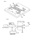
- a conventional directional coupler composed of microstrips shown in Fig. 6 is disclosed in Patent Document 1.
- This directional coupler is what is called a side-edge type coupler, which has a structure in which sections of respective stripline electrodes 81a and 82a of microstrips 81 and 82 are disposed close to each other for the length of ⁇ /4 in the horizontal direction and the upper and lower surfaces of the microstrips 81 and 82 are covered with ground electrodes 83 and 84.
- first microwave power is input from a port 1 to the microstrip 81 functioning as a main line
- second microwave power that is a fraction of the first microwave power is generated in a port 3 of the microstrip 82 functioning as a subordinate line.
- a main line 70a of a directional coupler 70 is disposed between a transmission power amplifier 71 and an antenna 72 and one end of a subordinate line 70b is connected to an automatic gain control circuit 73 so that the automatic gain control circuit 73 adjusts the output of the transmission power amplifier 71, as shown in Fig. 7.
- ⁇ /4 is 7.5 cm (on the condition that the specific inductive capacity is 1) at 1 GHz.
- the required minimum length of the sections of the stripline electrodes 81a and 82a is 7.5 cm, the sections being disposed close to each other in the horizontal direction. Accordingly, the size of the substrate, which includes the stripline electrodes 81a and 82a thereon, becomes large.
- the stripline electrodes having the length of a quarter of a wavelength are formed with the stripline electrode components and the via holes so that the stripline electrodes are divided into components on a plurality of laminated dielectric substrates.
- the size of the improved directional coupler can be small compared with that of the directional coupler shown in Fig. 6.
- the total length of the stripline electrodes is required to be a quarter of a wavelength.
- the size of the directional coupler cannot be largely reduced.
- side-edge type couplers have a problem in that it is difficult to achieve a high degree of coupling due to the characteristics of the distribution of a magnetic field around stripline electrodes.
- the improved directional coupler is also a coupler in which side-edge coupling between a pair of stripline electrodes is used.
- the improved directional coupler has a problem in that it is difficult to achieve a high degree of coupling.
- a directional coupler that is what is called a broad-side type coupler is proposed in Patent Document 2.
- spiral-shaped coupled lines are opposed to each other with dielectric layers therebetween so as to achieve coupling between the coupled lines. Since the inductance value of the coupled lines becomes high in this directional coupler, this directional coupler can be constructed with lines that are shorter than a quarter of a wavelength. Thus, the size can be readily reduced, and a high degree of coupling can be achieved with a small loss.
- a directional coupler includes at least one dielectric layer and two line electrodes that are formed on the at least one dielectric layer.
- the two line electrodes include an inner line electrode and an outer line electrode that surrounds the inner line electrode as viewed from the top. Corresponding currents are transmitted in the same direction through sections of the inner line electrode and the outer line electrode that are adjacent and parallel to each other.
- the inductance values of the line electrodes become high.
- inductive coupling between the inner line electrode and the outer line electrode becomes strong, and capacitive coupling between the inner line electrode and the outer line electrode becomes weak, thereby achieving high isolation.
- high inductance values can be achieved while the size of the directional coupler is small, and thus the size of the directional coupler can be reduced.
- the inductance values of the inner line electrode and the outer line electrode can be readily adjusted so that the inductance values agree with each other by adjusting the respective numbers of turns of the inner line electrode and the outer line electrode.
- a directional coupler includes at least one dielectric layer and two line electrodes that are formed on the at least one dielectric layer.
- the two line electrodes include a spiral-shaped or helical-shaped inner line electrode and a spiral-shaped or helical-shaped outer line electrode that surrounds the inner line electrode as viewed from the top.
- the inner line electrode and the outer line electrode are formed so as to have a spiral or helical shape.
- the corresponding currents are transmitted in the same direction through the sections of the inner line electrode and the outer line electrode, which are adjacent and parallel to each other, and the inductance values of the line electrodes become high.
- inductive coupling between the inner line electrode and the outer line electrode becomes strong, and capacitive coupling between the inner line electrode and the outer line electrode becomes weak, thereby achieving high isolation.
- high inductance values can be achieved while the size of the directional coupler is small, and thus the size of the directional coupler can be reduced.
- the inductance values of the inner line electrode and the outer line electrode can be readily adjusted so that the inductance values agree with each other by adjusting the respective numbers of turns of the inner line electrode and the outer line electrode.
- the length of each of the inner line electrode and the outer line electrode can be kept less than a quarter of a wavelength.
- the size of the directional coupler can be further reduced.
- the width of the inner line electrode is smaller than the width of the outer line electrode.
- the inductance value of the inner line electrode is increased. Accordingly, even when the number of turns of the inner line electrode is reduced, the inductance values of the inner line electrode and the outer line electrode can be adjusted so that the inductance values agree with each other. Thus, the size of the directional coupler can be further reduced.
- the number of turns of the inner line electrode may be larger than the number of turns of the outer line electrode.
- the inductance values of the inner line electrode and the outer line electrode can be readily adjusted so that the inductance values agree with each other by increasing the number of turns of the inner line electrode.
- the inner line electrode and the outer line electrode may be formed on the same plane.
- a first area of the spiral-shaped or helical-shaped outer line electrode opposing the spiral-shaped or helical-shaped inner line electrode, which is located inside the outer line electrode, is substantially the same as a second area of the inner edge of the innermost circumferential of the outer line electrode opposing the outer edge of the outermost circumferential of the inner line electrode.
- the thickness of the inner line electrode and the outer line electrode is fairly small.
- the capacitance formed between the inner line electrode and the outer line electrode is small, and the degree of isolation between these line electrodes can be significantly increased.
- the inner line electrode and the outer line electrode may be formed on different planes.
- the capacitance formed between the inner line electrode and the outer line electrode can be further reduced by forming the inner line electrode and the outer line electrode on different planes.
- the degree of isolation between these line electrodes can be further increased.
- At least one of the inner line electrode and the outer line electrode may be divided into line electrode components that are formed on a plurality of planes, and the divided line electrode components may be connected in series with each other through a via hole.
- the inner line electrode and/or the outer line electrode are divided into line electrode components that are formed on a plurality of planes, the number of line electrode components per unit area that are formed on one plane can be reduced. Thus, the size of the directional coupler can be further reduced.
- the directional coupler according to the present invention may further include a ground electrode that is formed on the dielectric layer. Capacitances may be formed between the ground electrode and individual ends of the inner line electrode and the outer line electrode. Due to the functions of the capacitances formed between the ground electrode and the individual ends of the inner line electrode and the outer line electrode, the resonant frequencies of the inner line electrode and the outer line electrode can be reduced. Thus, the size of the directional coupler can be further reduced by shortening the lengths of the line electrodes to obtain a predetermined resonant frequency.
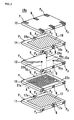
- Figs. 1 and 2 show the external appearance and the exploded structure of a directional coupler 10a according to a first embodiment of the present invention, respectively.
- the directional coupler 10a includes a chip laminate body 16 composed of a first ground electrode substrate 11, a dielectric substrate 12 that includes an inner line electrode 21a and an outer line electrode 22a that have a spiral shape and are described below on one major surface thereof, a lead-out conductor substrate 13 that includes lead-out conductors 23a, 24a, and 25a of the inner line electrode 21a and the outer line electrode 22a formed thereon, a second ground electrode substrate 14, and a protection substrate 15.
- External electrodes G for grounding, external electrodes P 1 and P 2 for a main line, and external electrodes P 3 and P 4 for a subordinate line are formed on side surfaces of the laminate body 16 so as to extend from the first ground electrode substrate 11 to the protection substrate 15.
- the aforementioned substrates 11, 12, 13, 14, and 15 are composed of ceramic green sheets that are formed of dielectric ceramic materials by using, for example, the doctor blade method or the Czochralski method, and are laminated into the laminate body 16 and sintered.
- separating line does not appear between the substrates 11, 12, 13, 14, and 15 in the direction in which these substrates are laminated.
- the aforementioned external electrodes G, P 1 P 2 , P 3 , and P 4 may be formed after the laminate body 16 has been sintered.
- a ground electrode 17 is formed on the major surface of the first ground electrode substrate 11.
- the size of the ground electrode 17 is such that the ground electrode 17 completely covers the inner line electrode 21a and the outer line electrode 22a, which have a spiral shape and are formed on the dielectric substrate 12, excluding the peripheral region of the major surface of the first ground electrode substrate 11.
- the ground electrode 17 is connected to the external electrodes G, G for grounding through lead-out parts 17a, 17a.
- the inner line electrode 21a functioning as a main line and the outer line electrode 22a functioning as a subordinate line, these line electrodes having a spiral shape, are formed by printing on the major surface of the dielectric substrate 12 at a stage at which the dielectric substrate 12 is a green sheet that has not been sintered.
- the inner line electrode 21a and the outer line electrode 22a have the same width, and the respective numbers of turns of the inner line electrode 21a and the outer line electrode 22a are 2.5 and 1.5.
- the line length of each of the main and subordinate lines is less than a quarter of a wavelength.
- the lead-out conductors 23a, 24a, and 25a are formed on the major surface of the lead-out conductor substrate 13.
- the inner end of the inner line electrode 21a having a spiral shape is connected to the external electrode P 1 for the main line through a via hole Vh 1 and the lead-out conductor 23a, which are formed in the lead-out conductor substrate 13, and the outer end of the inner line electrode 21a is connected to the external electrode P 2 for the main line through a via hole Vh 2 and the lead-out conductor 24a, which are formed in the lead-out conductor substrate 13.
- the inner end of the outer line electrode 22a having a spiral shape is connected to the external electrode P 3 for the subordinate line through a via hole Vh 3 and the lead-out conductor 25a, which are formed in the lead-out conductor substrate 13, and the outer end of the outer line electrode 22a is connected directly to the external electrode P 4 for the subordinate line on the dielectric substrate 12.
- a ground electrode 18 is formed on the major surface of the second ground electrode substrate 14 laminated on the lead-out conductor substrate 13, as with the first ground electrode substrate 11.
- the size of the ground electrode 18 is such that the ground electrode 18 completely covers the two line electrodes 21a and 22a, which have a spiral shape and are formed on the dielectric substrate 12, excluding the peripheral region of the major surface of the second ground electrode substrate 14.
- the ground electrode 18 is connected to the external electrodes G for grounding through lead-out parts 18a.
- the ground electrode 18 is covered with the protection substrate 15 laminated on the second ground electrode substrate 14.
- the outer line electrode 22a having a spiral shape and the inner line electrode 21a having a spiral shape are coupled by side-edge coupling therebetween.
- the inner line electrode 21a is surrounded by the outer line electrode 22a and disposed inside the outer line electrode 22a.
- An enclosed area that is enclosed between the inner line electrode 21a and the outer line electrode 22a is substantially the same as an enclosed area that is enclosed between the inner edge of the innermost circumferential of the outer line electrode 22a and the outer edge of the outermost circumferential of the inner line electrode 21a.
- the inner line electrode 21a and the outer line electrode 22a are formed by printing, the thickness of each line electrode is thin. Thus, the capacitance formed between the inner line electrode 21a and the outer line electrode 22a is small, and high isolation between these line electrodes can be achieved.
- the inner line electrode 21a and the outer line electrode 22a have a spiral shape, and, according to a neighboring parallel area, for example, in Fig. 2, the corresponding currents are transmitted through front left sections of the inner line electrode 21a and the outer line electrode 22a in the same direction indicated by an arrow A.
- the inductance values of the line electrodes 21a and 22a become high at sections of the inner line electrode 21a and the outer line electrode 22a. Accordingly, inductive coupling between the inner line electrode 21a and the outer line electrode 22a becomes strong and capacitive coupling between the inner line electrode 21a and the outer line electrode 22a becomes weak.
- the inductance values of the inner line electrode 21a and the outer line electrode 22a can be readily adjusted so that the inductance values agree with each other by adjusting the respective numbers of turns of the inner line electrode 21a and the outer line electrode 22a.
- the inner line electrode 21a and the outer line electrode 22a have a spiral shape, and the corresponding currents are transmitted through the sections of the inner line electrode 21a and the outer line electrode 22a that are parallel and adjacent to each other in the same direction.
- a high inductance value can be achieved while the size of the directional coupler 10a is small.
- the length of each line electrode can be set to less than a quarter of a wavelength, and the size of the directional coupler 10a can be reduced.
- the inner line electrode 21a is the main line electrode and the outer line electrode 22a is the subordinate line electrode. Even when the inner line electrode 21a is the subordinate line and the outer line electrode 22a is the main line, the directional coupler 10a can operate in the same manner. The same applies to the embodiments, which are described below.
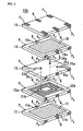
- Fig. 3 shows a directional coupler 10b according to a second embodiment of the present invention. While the dielectric substrate 12 is used in the directional coupler 10a according to the first embodiment, which was described with reference to Figs. 1 and 2, the inner line electrode 21a and the outer line electrode 22a having the same width being formed on the dielectric substrate 12, a dielectric substrate 12a is used in the directional coupler 10b, an inner line electrode 21b and an outer line electrode 22b being formed on the dielectric substrate 12a so that the width of the inner line electrode 21b is narrower than that of the outer line electrode 22b.
- the width of the inner line electrode 21b is narrowed in this way, the inductance value of the inner line electrode 21b is increased. Accordingly, the number of turns of the inner line electrode 21b can be reduced. Thus, a directional coupler that is smaller than the directional coupler 10a can be obtained as the directional coupler 10b.
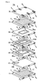
- Fig. 4 shows a directional coupler according to a third embodiment of the present invention. While the dielectric substrate 12 is used in the directional coupler 10a according to the first embodiment, which was described with reference to Figs. 1 and 2, the inner line electrode 21a and the outer line electrode 22a having the same width being formed on the dielectric substrate 12, dielectric substrates 32, 33, and 34 are used in the directional coupler 10c, three inner line electrode components 21aa, 21ab, and 21ac, into which the inner line electrode is divided, being respectively formed on the dielectric substrates 32, 33, and 34, two outer line electrode components 22aa and 22ab, into which the outer line electrode is divided, being respectively formed on the dielectric substrates 32 and 33. When this arrangement is adopted, the inner line electrode and the outer line electrode are formed as helical lines.
- One end of the inner line electrode component 21aa is connected through a via hole Vh 11 that is formed in the dielectric substrate 32 to a lead-out conductor 23b that is formed on a lead-out conductor substrate 31 and connected to the external electrode P 1 for the main line.
- the other end of the inner line electrode component 21aa is connected through a via hole Vh 12 that is formed in the dielectric substrate 33 to one end of the inner line electrode component 21ab that is formed on the dielectric substrate 33.
- the other end of the inner line electrode component 21ab is connected through a via hole Vh 13 that is formed in the dielectric substrate 34 to one end of the inner line electrode component 21ac that is formed on the dielectric substrate 34.
- the other end of the inner line electrode component 21ac is connected directly to the external electrode P 2 for the main line on the dielectric substrate 34.
- one end of the outer line electrode component 22aa is connected directly to the external electrode P 3 for the subordinate line on the dielectric substrate 32.
- the other end of the outer line electrode component 22aa is connected through a via hole Vh 14 that is formed in the dielectric substrate 33 to one end of the outer line electrode component 22ab that is formed on the dielectric substrate 33.
- the other end of the outer line electrode component 22ab is connected directly to the external electrode P 4 for the subordinate line on the dielectric substrate 33.
- the inner line electrode is divided into the three outer line electrode components 21aa, 21ab, and 21ac, and the outer line electrode is divided into the two outer line electrode components 22aa and 22ab.
- the number of line electrode components per unit area that are formed on the dielectric substrates 32, 33, and 34 can be reduced, and the size of the directional coupler can be further reduced.
- Fig. 5 shows a directional coupler 10d according to a fourth embodiment of the present invention.
- the inner line electrode is divided into three inner line electrode components 21aa, 21ab, and 21ac
- the outer line electrode is divided into three outer line electrode components 22aa, 22ab, and 22ac, as in the directional coupler 10c according to the third embodiment, which was described with reference to Fig. 4.
- These line electrode components are formed on three dielectric substrates 57, 58, and 59.
- Capacitances are formed between the external electrodes P 1 to P 4 for the main and subordinate lines and the external electrodes G for grounding.
- One end of the inner line electrode component 21aa is connected through a via hole Vh 21 that is formed in the dielectric substrate 57 to a lead-out conductor 23c that is formed on a lead-out conductor substrate 56 and connected to the external electrode P 1 for the main line.
- the other end of the inner line electrode component 21aa is connected through a via hole Vh 22 that is formed in the dielectric substrate 58 to one end of the inner line electrode component 21ab that is formed on the dielectric substrate 58.
- the other end of the inner line electrode component 21ab is connected through a via hole Vh 23 that is formed in the dielectric substrate 59 to one end of the inner line electrode component 21ac that is formed on the dielectric substrate 59.
- the other end of the inner line electrode component 21ac is connected directly to the external electrode P 2 for the main line on the dielectric substrate 59.
- one end of the outer line electrode component 22aa is connected through a via hole Vh 24 that is formed in the dielectric substrate 57 to a lead-out conductor 26 that is formed on the lead-out conductor substrate 56 and connected to the external electrode P 4 for the subordinate line.
- the other end of the outer line electrode component 22aa is connected through a via hole Vh 25 that is formed in the dielectric substrate 58 to one end of the outer line electrode component 22ab that is formed on the dielectric substrate 58.
- the other end of the outer line electrode component 22ab is connected through a via hole Vh 26 that is formed in the dielectric substrate 59 to one end of the outer line electrode component 22ac that is formed on the dielectric substrate 59.
- the other end of the outer line electrode component 22ac is connected directly to the external electrode P 3 for the subordinate line on the dielectric substrate 59.
- a dummy substrate 55a is laminated between the lead-out conductor substrate 56 and the ground electrode substrate 11, and a dummy substrate 55b is laminated between the dielectric substrate 59 and the ground electrode substrate 14.
- capacitor electrode substrates 51 to 54 for forming capacitances are laminated under the ground electrode substrate 11 in this order from the bottom.
- a capacitor electrode 61 is formed on the major surface of the capacitor electrode substrate 51.
- the capacitor electrode 61 is formed so that the capacitor electrode 61 covers a substantially whole area of the major surface of the capacitor electrode substrate 51, excluding the peripheral region of the major surface of the capacitor electrode substrate 51.
- the capacitor electrode 61 is connected to the external electrodes G,G for grounding through lead-out parts 61a, 61a.
- Two strip-shaped capacitor electrodes 63b and 64b are formed on the major surface of the capacitor electrode substrate 52.
- the capacitor electrodes 63b and 64b are connected to the external electrodes P 4 and P 3 for the subordinate line, respectively.
- a capacitor electrode 62 is formed on the major surface of the capacitor electrode substrate 53.
- the capacitor electrode 62 is formed so that the capacitor electrode 62 covers a substantially whole area of the major surface of the capacitor electrode substrate 53, excluding the peripheral region of the major surface of the capacitor electrode substrate 53.
- the capacitor electrode 62 is connected to the external electrodes G for grounding through lead-out parts 62a.
- Two strip-shaped capacitor electrodes 63a and 64a are formed on the major surface of the capacitor electrode substrate 54.
- the capacitor electrodes 63a and 64a are connected to the external electrodes P 1 and P 2 for the main line, respectively.
- the advantages achieved by the fourth embodiment are the same as those achieved by the first embodiment. Moreover, when the aforementioned arrangement is adopted, capacitances are formed between the capacitor electrodes 63a and 64a, the capacitor electrode 62, and the ground electrode 17, and between the capacitor electrodes 63b and 64b, the capacitor electrode 61, and the capacitor electrode 62. Due to the functions of these capacitances, the resonant frequencies of the inner line electrode, which is divided into the three inner line electrode components 21aa, 21ab, and 21ac, and the outer line electrode, which is divided into the three outer line electrode components 22aa, 22ab, and 22ac, can be reduced. Thus, the size of the directional coupler 10d can be further reduced by shortening the lengths of the line electrodes to obtain a predetermined resonant frequency.
- Directional couplers according to the present invention are not limited to the aforementioned embodiments and can have various structures within the gist of the present invention.
- the inner line electrode 21a may be formed on one dielectric substrate, and the outer line electrode 22a may be formed on another dielectric substrate.
- the capacitance between the inner line electrode 21a and the outer line electrode 22a can be reduced, resulting in high isolation between these line electrodes.
- the present invention can be applied to directional couplers for a microwave band as described above, and in particular, is excellent in that a high coupling value and high isolation characteristics can be achieved.
Landscapes
- Control Of Motors That Do Not Use Commutators (AREA)
- Coils Or Transformers For Communication (AREA)
- Waveguides (AREA)
- Paper (AREA)
- Compositions Of Oxide Ceramics (AREA)
- Preparation Of Compounds By Using Micro-Organisms (AREA)
Abstract
Description
- The present invention relates to directional couplers, and in particular, relates to a directional coupler that couples to only microwaves that propagate through a transmission line in one direction and obtains an output proportional to the microwave power and that does not couple to microwaves that propagate through the transmission line in another direction opposite to the one direction.
- For example, as described in
Patent Document 1, waveguide circuits, which have been predominant microwave circuits, require high precision machining and thus are not suitable for mass production and are expensive. Moreover, a problem has existed with waveguide circuits, in that the outer sizes and weights of waveguide circuits are large. Thus, microstrips, which can be reduced in size and weight through the use of large-scale integration technology, have been used in radios, BS receivers, and the like. - A conventional directional coupler composed of microstrips shown in Fig. 6 is disclosed in
Patent Document 1. This directional coupler is what is called a side-edge type coupler, which has a structure in which sections ofrespective stripline electrodes 81a and 82a ofmicrostrips microstrips ground electrodes stripline electrodes 81a and 82a, the sections being disposed close to each other, while first microwave power is input from aport 1 to themicrostrip 81 functioning as a main line, second microwave power that is a fraction of the first microwave power is generated in aport 3 of themicrostrip 82 functioning as a subordinate line. - For example, in a cellular phone unit, in order to keep the transmission power at the minimum level through the use of the function of dividing high frequency signals into two components in the aforementioned directional coupler, a
main line 70a of adirectional coupler 70 is disposed between a transmission power amplifier 71 and anantenna 72 and one end of asubordinate line 70b is connected to an automaticgain control circuit 73 so that the automaticgain control circuit 73 adjusts the output of the transmission power amplifier 71, as shown in Fig. 7. - With regard to cellular phone units and the like, an important issue is to minimize the size. Thus, the sizes of directional couplers have been required to be further reduced. However, in the directional coupler shown in Fig. 6, for example, λ/4 is 7.5 cm (on the condition that the specific inductive capacity is 1) at 1 GHz. Thus, the required minimum length of the sections of the
stripline electrodes 81a and 82a is 7.5 cm, the sections being disposed close to each other in the horizontal direction. Accordingly, the size of the substrate, which includes thestripline electrodes 81a and 82a thereon, becomes large. Moreover, for example, when respective substrates that include theground electrodes stripline electrodes 81a and 82a thereon, a problem arises in that reduction in size is limited and the cost increases. - Accordingly, a directional coupler that is improved to solve the aforementioned problem is proposed in
Patent Document 1. In this directional coupler, ground electrode substrates that include ground electrodes thereon and dielectric substrates on which a pair of stripline electrodes are formed so that the stripline electrodes are disposed close and parallel to each other in a spiral shape are alternately laminated. Then, the corresponding stripline electrode components of the individual dielectric substrates are connected in series with each other through a pair of via holes that are close to each other so that stripline electrodes having the length of a quarter of a wavelength are formed. - In the improved directional coupler, the stripline electrodes having the length of a quarter of a wavelength are formed with the stripline electrode components and the via holes so that the stripline electrodes are divided into components on a plurality of laminated dielectric substrates. Thus, the size of the improved directional coupler can be small compared with that of the directional coupler shown in Fig. 6. However, even in the improved directional coupler, the total length of the stripline electrodes is required to be a quarter of a wavelength. Thus, the size of the directional coupler cannot be largely reduced. Moreover, in general, side-edge type couplers have a problem in that it is difficult to achieve a high degree of coupling due to the characteristics of the distribution of a magnetic field around stripline electrodes. The improved directional coupler is also a coupler in which side-edge coupling between a pair of stripline electrodes is used. Thus, the improved directional coupler has a problem in that it is difficult to achieve a high degree of coupling.
- On the other hand, a directional coupler that is what is called a broad-side type coupler is proposed in
Patent Document 2. In this directional coupler, spiral-shaped coupled lines are opposed to each other with dielectric layers therebetween so as to achieve coupling between the coupled lines. Since the inductance value of the coupled lines becomes high in this directional coupler, this directional coupler can be constructed with lines that are shorter than a quarter of a wavelength. Thus, the size can be readily reduced, and a high degree of coupling can be achieved with a small loss. - However, in the directional coupler disclosed in
Patent Document 2, since spiral-shaped coupled lines are opposed to each other with dielectric layers therebetween so as to achieve coupling between the coupled lines, the capacitance between the coupled lines becomes large. Thus, this directional coupler has a problem in that high isolation between the coupled lines cannot be achieved. - Moreover, in the directional couplers disclosed in
Patent Documents - [Patent Document 1]
Japanese Unexamined Patent Application Publication No. 5-160614 - [Patent Document 2]
Japanese Patent No. 3203253 - Accordingly, it is an object of the present invention to provide a small directional coupler that has a high coupling value and high isolation characteristics.
- To achieve the aforementioned object, a directional coupler according to a first aspect of the present invention includes at least one dielectric layer and two line electrodes that are formed on the at least one dielectric layer. The two line electrodes include an inner line electrode and an outer line electrode that surrounds the inner line electrode as viewed from the top. Corresponding currents are transmitted in the same direction through sections of the inner line electrode and the outer line electrode that are adjacent and parallel to each other.
- In the directional coupler according to the first aspect of the present invention, since the corresponding currents are transmitted in the same direction through the sections of the inner line electrode and the outer line electrode, which are adjacent and parallel to each other, the inductance values of the line electrodes become high. Thus, inductive coupling between the inner line electrode and the outer line electrode becomes strong, and capacitive coupling between the inner line electrode and the outer line electrode becomes weak, thereby achieving high isolation. Moreover, high inductance values can be achieved while the size of the directional coupler is small, and thus the size of the directional coupler can be reduced. Moreover, the inductance values of the inner line electrode and the outer line electrode can be readily adjusted so that the inductance values agree with each other by adjusting the respective numbers of turns of the inner line electrode and the outer line electrode.
- A directional coupler according to a second aspect of the present invention includes at least one dielectric layer and two line electrodes that are formed on the at least one dielectric layer. The two line electrodes include a spiral-shaped or helical-shaped inner line electrode and a spiral-shaped or helical-shaped outer line electrode that surrounds the inner line electrode as viewed from the top.
- In the directional coupler according to the second aspect of the present invention, the inner line electrode and the outer line electrode are formed so as to have a spiral or helical shape. Thus, the corresponding currents are transmitted in the same direction through the sections of the inner line electrode and the outer line electrode, which are adjacent and parallel to each other, and the inductance values of the line electrodes become high. Thus, inductive coupling between the inner line electrode and the outer line electrode becomes strong, and capacitive coupling between the inner line electrode and the outer line electrode becomes weak, thereby achieving high isolation. Moreover, high inductance values can be achieved while the size of the directional coupler is small, and thus the size of the directional coupler can be reduced. Moreover, the inductance values of the inner line electrode and the outer line electrode can be readily adjusted so that the inductance values agree with each other by adjusting the respective numbers of turns of the inner line electrode and the outer line electrode.
- In the directional couplers according to the first and second aspects of the present invention, since the degree of inductive coupling between the inner line electrode and the outer line electrode is high, the length of each of the inner line electrode and the outer line electrode can be kept less than a quarter of a wavelength. Thus, the size of the directional coupler can be further reduced.
- Moreover, in the directional couplers according to the first and second aspects of the present invention, it is preferable that the width of the inner line electrode is smaller than the width of the outer line electrode. When the width of the inner line electrode is reduced, the inductance value of the inner line electrode is increased. Accordingly, even when the number of turns of the inner line electrode is reduced, the inductance values of the inner line electrode and the outer line electrode can be adjusted so that the inductance values agree with each other. Thus, the size of the directional coupler can be further reduced.
- Moreover, the number of turns of the inner line electrode may be larger than the number of turns of the outer line electrode. The inductance values of the inner line electrode and the outer line electrode can be readily adjusted so that the inductance values agree with each other by increasing the number of turns of the inner line electrode.
- Moreover, the inner line electrode and the outer line electrode may be formed on the same plane. A first area of the spiral-shaped or helical-shaped outer line electrode opposing the spiral-shaped or helical-shaped inner line electrode, which is located inside the outer line electrode, is substantially the same as a second area of the inner edge of the innermost circumferential of the outer line electrode opposing the outer edge of the outermost circumferential of the inner line electrode. Thus, only certain sections of the inner line electrode oppose sections of the outer line electrode in the first area. Moreover, the thickness of the inner line electrode and the outer line electrode is fairly small. Thus, the capacitance formed between the inner line electrode and the outer line electrode is small, and the degree of isolation between these line electrodes can be significantly increased.
- Moreover, the inner line electrode and the outer line electrode may be formed on different planes. The capacitance formed between the inner line electrode and the outer line electrode can be further reduced by forming the inner line electrode and the outer line electrode on different planes. Thus, the degree of isolation between these line electrodes can be further increased.
- Moreover, at least one of the inner line electrode and the outer line electrode may be divided into line electrode components that are formed on a plurality of planes, and the divided line electrode components may be connected in series with each other through a via hole. When the inner line electrode and/or the outer line electrode are divided into line electrode components that are formed on a plurality of planes, the number of line electrode components per unit area that are formed on one plane can be reduced. Thus, the size of the directional coupler can be further reduced.
- Moreover, the directional coupler according to the present invention may further include a ground electrode that is formed on the dielectric layer. Capacitances may be formed between the ground electrode and individual ends of the inner line electrode and the outer line electrode. Due to the functions of the capacitances formed between the ground electrode and the individual ends of the inner line electrode and the outer line electrode, the resonant frequencies of the inner line electrode and the outer line electrode can be reduced. Thus, the size of the directional coupler can be further reduced by shortening the lengths of the line electrodes to obtain a predetermined resonant frequency.
-
- Fig. 1 is a perspective view showing the external appearance of a directional coupler according to a first embodiment of the present invention.
- Fig. 2 is an exploded perspective view showing the structure of the directional coupler shown in Fig. 1.
- Fig. 3 is an exploded perspective view of a directional coupler according to a second embodiment of the present invention.
- Fig. 4 is an exploded perspective view of a directional coupler according to a third embodiment of the present invention.
- Fig. 5 is an exploded perspective view of a directional coupler according to a fourth embodiment of the present invention.
- Fig. 6 shows a conventional directional coupler.
- Fig. 7 is a block diagram showing an RF transmitter circuit in which a directional coupler is used.
- Directional couplers according to embodiments of the present invention will now be described with reference to the attached drawings.
- Figs. 1 and 2 show the external appearance and the exploded structure of a directional coupler 10a according to a first embodiment of the present invention, respectively. The directional coupler 10a includes a chip laminate body 16 composed of a first
ground electrode substrate 11, adielectric substrate 12 that includes aninner line electrode 21a and anouter line electrode 22a that have a spiral shape and are described below on one major surface thereof, a lead-out conductor substrate 13 that includes lead-out conductors 23a, 24a, and 25a of theinner line electrode 21a and theouter line electrode 22a formed thereon, a secondground electrode substrate 14, and aprotection substrate 15. - External electrodes G for grounding, external electrodes P1 and P2 for a main line, and external electrodes P3 and P4 for a subordinate line are formed on side surfaces of the laminate body 16 so as to extend from the first
ground electrode substrate 11 to theprotection substrate 15. - The
aforementioned substrates - Thus, in practice, in Fig. 1, separating line does not appear between the
substrates - A
ground electrode 17 is formed on the major surface of the firstground electrode substrate 11. The size of theground electrode 17 is such that theground electrode 17 completely covers theinner line electrode 21a and theouter line electrode 22a, which have a spiral shape and are formed on thedielectric substrate 12, excluding the peripheral region of the major surface of the firstground electrode substrate 11. Theground electrode 17 is connected to the external electrodes G, G for grounding through lead-outparts - The
inner line electrode 21a functioning as a main line and theouter line electrode 22a functioning as a subordinate line, these line electrodes having a spiral shape, are formed by printing on the major surface of thedielectric substrate 12 at a stage at which thedielectric substrate 12 is a green sheet that has not been sintered. In the first embodiment, theinner line electrode 21a and theouter line electrode 22a have the same width, and the respective numbers of turns of theinner line electrode 21a and theouter line electrode 22a are 2.5 and 1.5. The line length of each of the main and subordinate lines is less than a quarter of a wavelength. - The lead-out conductors 23a, 24a, and 25a are formed on the major surface of the lead-
out conductor substrate 13. The inner end of theinner line electrode 21a having a spiral shape is connected to the external electrode P1 for the main line through a via hole Vh1 and the lead-out conductor 23a, which are formed in the lead-out conductor substrate 13, and the outer end of theinner line electrode 21a is connected to the external electrode P2 for the main line through a via hole Vh2 and the lead-out conductor 24a, which are formed in the lead-out conductor substrate 13. - The inner end of the
outer line electrode 22a having a spiral shape is connected to the external electrode P3 for the subordinate line through a via hole Vh3 and the lead-out conductor 25a, which are formed in the lead-out conductor substrate 13, and the outer end of theouter line electrode 22a is connected directly to the external electrode P4 for the subordinate line on thedielectric substrate 12. - A
ground electrode 18 is formed on the major surface of the secondground electrode substrate 14 laminated on the lead-out conductor substrate 13, as with the firstground electrode substrate 11. The size of theground electrode 18 is such that theground electrode 18 completely covers the twoline electrodes dielectric substrate 12, excluding the peripheral region of the major surface of the secondground electrode substrate 14. Theground electrode 18 is connected to the external electrodes G for grounding through lead-outparts 18a. Theground electrode 18 is covered with theprotection substrate 15 laminated on the secondground electrode substrate 14. - In the directional coupler 10a having the aforementioned structure, the
outer line electrode 22a having a spiral shape and theinner line electrode 21a having a spiral shape are coupled by side-edge coupling therebetween. Theinner line electrode 21a is surrounded by theouter line electrode 22a and disposed inside theouter line electrode 22a. An enclosed area that is enclosed between theinner line electrode 21a and theouter line electrode 22a is substantially the same as an enclosed area that is enclosed between the inner edge of the innermost circumferential of theouter line electrode 22a and the outer edge of the outermost circumferential of theinner line electrode 21a. Thus, only certain sections of theinner line electrode 21a oppose sections of theouter line electrode 22a in the first area. Moreover, since theinner line electrode 21a and theouter line electrode 22a are formed by printing, the thickness of each line electrode is thin. Thus, the capacitance formed between theinner line electrode 21a and theouter line electrode 22a is small, and high isolation between these line electrodes can be achieved. - Moreover, in the directional coupler 10a, the
inner line electrode 21a and theouter line electrode 22a have a spiral shape, and, according to a neighboring parallel area, for example, in Fig. 2, the corresponding currents are transmitted through front left sections of theinner line electrode 21a and theouter line electrode 22a in the same direction indicated by an arrow A. Thus, the inductance values of theline electrodes inner line electrode 21a and theouter line electrode 22a. Accordingly, inductive coupling between theinner line electrode 21a and theouter line electrode 22a becomes strong and capacitive coupling between theinner line electrode 21a and theouter line electrode 22a becomes weak. Moreover, the inductance values of theinner line electrode 21a and theouter line electrode 22a can be readily adjusted so that the inductance values agree with each other by adjusting the respective numbers of turns of theinner line electrode 21a and theouter line electrode 22a. - That is to say, in the directional coupler 10a, the
inner line electrode 21a and theouter line electrode 22a have a spiral shape, and the corresponding currents are transmitted through the sections of theinner line electrode 21a and theouter line electrode 22a that are parallel and adjacent to each other in the same direction. Thus, a high inductance value can be achieved while the size of the directional coupler 10a is small. The length of each line electrode can be set to less than a quarter of a wavelength, and the size of the directional coupler 10a can be reduced. - In the aforementioned description of the directional coupler 10a, the
inner line electrode 21a is the main line electrode and theouter line electrode 22a is the subordinate line electrode. Even when theinner line electrode 21a is the subordinate line and theouter line electrode 22a is the main line, the directional coupler 10a can operate in the same manner. The same applies to the embodiments, which are described below. - Fig. 3 shows a
directional coupler 10b according to a second embodiment of the present invention. While thedielectric substrate 12 is used in the directional coupler 10a according to the first embodiment, which was described with reference to Figs. 1 and 2, theinner line electrode 21a and theouter line electrode 22a having the same width being formed on thedielectric substrate 12, adielectric substrate 12a is used in thedirectional coupler 10b, an inner line electrode 21b and anouter line electrode 22b being formed on thedielectric substrate 12a so that the width of the inner line electrode 21b is narrower than that of theouter line electrode 22b. - When the width of the inner line electrode 21b is narrowed in this way, the inductance value of the inner line electrode 21b is increased. Accordingly, the number of turns of the inner line electrode 21b can be reduced. Thus, a directional coupler that is smaller than the directional coupler 10a can be obtained as the
directional coupler 10b. - In Fig. 3, the same reference letters and numerals as in Fig. 2 are assigned to the corresponding components, and duplicated description is omitted. The advantages achieved by the second embodiment are basically the same as those achieved by the first embodiment.
- Fig. 4 shows a directional coupler according to a third embodiment of the present invention. While the
dielectric substrate 12 is used in the directional coupler 10a according to the first embodiment, which was described with reference to Figs. 1 and 2, theinner line electrode 21a and theouter line electrode 22a having the same width being formed on thedielectric substrate 12,dielectric substrates directional coupler 10c, three inner line electrode components 21aa, 21ab, and 21ac, into which the inner line electrode is divided, being respectively formed on thedielectric substrates dielectric substrates - In Fig. 4, the same reference letters and numerals as in Fig. 2 are assigned to the corresponding components, and duplicated description is omitted.
- One end of the inner line electrode component 21aa is connected through a via hole Vh11 that is formed in the
dielectric substrate 32 to a lead-outconductor 23b that is formed on a lead-out conductor substrate 31 and connected to the external electrode P1 for the main line. The other end of the inner line electrode component 21aa is connected through a via hole Vh12 that is formed in thedielectric substrate 33 to one end of the inner line electrode component 21ab that is formed on thedielectric substrate 33. - The other end of the inner line electrode component 21ab is connected through a via hole Vh13 that is formed in the
dielectric substrate 34 to one end of the inner line electrode component 21ac that is formed on thedielectric substrate 34. The other end of the inner line electrode component 21ac is connected directly to the external electrode P2 for the main line on thedielectric substrate 34. - On the other hand, one end of the outer line electrode component 22aa is connected directly to the external electrode P3 for the subordinate line on the
dielectric substrate 32. The other end of the outer line electrode component 22aa is connected through a via hole Vh14 that is formed in thedielectric substrate 33 to one end of the outer line electrode component 22ab that is formed on thedielectric substrate 33. The other end of the outer line electrode component 22ab is connected directly to the external electrode P4 for the subordinate line on thedielectric substrate 33. - Even when this arrangement is adopted, the same advantages as in the directional coupler 10a, which was described with reference to Figs. 1 and 2, can be achieved. As is apparent from Fig. 4, the inner line electrode is divided into the three outer line electrode components 21aa, 21ab, and 21ac, and the outer line electrode is divided into the two outer line electrode components 22aa and 22ab. Thus, the number of line electrode components per unit area that are formed on the
dielectric substrates - Fig. 5 shows a
directional coupler 10d according to a fourth embodiment of the present invention. In thedirectional coupler 10d, the inner line electrode is divided into three inner line electrode components 21aa, 21ab, and 21ac, and the outer line electrode is divided into three outer line electrode components 22aa, 22ab, and 22ac, as in thedirectional coupler 10c according to the third embodiment, which was described with reference to Fig. 4. These line electrode components are formed on threedielectric substrates - One end of the inner line electrode component 21aa is connected through a via hole Vh21 that is formed in the
dielectric substrate 57 to a lead-outconductor 23c that is formed on a lead-out conductor substrate 56 and connected to the external electrode P1 for the main line. The other end of the inner line electrode component 21aa is connected through a via hole Vh22 that is formed in thedielectric substrate 58 to one end of the inner line electrode component 21ab that is formed on thedielectric substrate 58. The other end of the inner line electrode component 21ab is connected through a via hole Vh23 that is formed in thedielectric substrate 59 to one end of the inner line electrode component 21ac that is formed on thedielectric substrate 59. The other end of the inner line electrode component 21ac is connected directly to the external electrode P2 for the main line on thedielectric substrate 59. - On the other hand, one end of the outer line electrode component 22aa is connected through a via hole Vh24 that is formed in the
dielectric substrate 57 to a lead-out conductor 26 that is formed on the lead-out conductor substrate 56 and connected to the external electrode P4 for the subordinate line. The other end of the outer line electrode component 22aa is connected through a via hole Vh25 that is formed in thedielectric substrate 58 to one end of the outer line electrode component 22ab that is formed on thedielectric substrate 58. The other end of the outer line electrode component 22ab is connected through a via hole Vh26 that is formed in thedielectric substrate 59 to one end of the outer line electrode component 22ac that is formed on thedielectric substrate 59. The other end of the outer line electrode component 22ac is connected directly to the external electrode P3 for the subordinate line on thedielectric substrate 59. - A dummy substrate 55a is laminated between the lead-
out conductor substrate 56 and theground electrode substrate 11, and adummy substrate 55b is laminated between thedielectric substrate 59 and theground electrode substrate 14. In thedirectional coupler 10d,capacitor electrode substrates 51 to 54 for forming capacitances are laminated under theground electrode substrate 11 in this order from the bottom. - A
capacitor electrode 61 is formed on the major surface of thecapacitor electrode substrate 51. Thecapacitor electrode 61 is formed so that thecapacitor electrode 61 covers a substantially whole area of the major surface of thecapacitor electrode substrate 51, excluding the peripheral region of the major surface of thecapacitor electrode substrate 51. Thecapacitor electrode 61 is connected to the external electrodes G,G for grounding through lead-outparts capacitor electrodes capacitor electrode substrate 52. Thecapacitor electrodes - A
capacitor electrode 62 is formed on the major surface of thecapacitor electrode substrate 53. Thecapacitor electrode 62 is formed so that thecapacitor electrode 62 covers a substantially whole area of the major surface of thecapacitor electrode substrate 53, excluding the peripheral region of the major surface of thecapacitor electrode substrate 53. Thecapacitor electrode 62 is connected to the external electrodes G for grounding through lead-outparts 62a. Two strip-shapedcapacitor electrodes capacitor electrode substrate 54. Thecapacitor electrodes - The advantages achieved by the fourth embodiment are the same as those achieved by the first embodiment. Moreover, when the aforementioned arrangement is adopted, capacitances are formed between the
capacitor electrodes capacitor electrode 62, and theground electrode 17, and between thecapacitor electrodes capacitor electrode 61, and thecapacitor electrode 62. Due to the functions of these capacitances, the resonant frequencies of the inner line electrode, which is divided into the three inner line electrode components 21aa, 21ab, and 21ac, and the outer line electrode, which is divided into the three outer line electrode components 22aa, 22ab, and 22ac, can be reduced. Thus, the size of thedirectional coupler 10d can be further reduced by shortening the lengths of the line electrodes to obtain a predetermined resonant frequency. - Directional couplers according to the present invention are not limited to the aforementioned embodiments and can have various structures within the gist of the present invention.
- For example, in the directional coupler 10a, although not specifically shown in the drawings, the
inner line electrode 21a may be formed on one dielectric substrate, and theouter line electrode 22a may be formed on another dielectric substrate. In this arrangement, the capacitance between theinner line electrode 21a and theouter line electrode 22a can be reduced, resulting in high isolation between these line electrodes. - The present invention can be applied to directional couplers for a microwave band as described above, and in particular, is excellent in that a high coupling value and high isolation characteristics can be achieved.
Claims (9)
- A directional coupler comprising at least one dielectric layer and two line electrodes that are formed on the at least one dielectric layer,
the two line electrodes comprising an inner line electrode and an outer line electrode that surrounds the inner line electrode as viewed from the top,
wherein corresponding currents are transmitted in the same direction through sections of the inner line electrode and the outer line electrode that are adjacent and parallel to each other. - A directional coupler comprising at least one dielectric layer and two line electrodes that are formed on the at least one dielectric layer,
the two line electrodes comprising a spiral-shaped or helical-shaped inner line electrode and a spiral-shaped or helical-shaped outer line electrode that surrounds the inner line electrode as viewed from the top. - The directional coupler according to Claim 1 or 2,
wherein the length of each of the inner line electrode and the outer line electrode is less than a quarter of a wavelength. - The directional coupler according to Claim 1, 2, or 3,
wherein the width of the inner line electrode is smaller than the width of the outer line electrode. - The directional coupler according to Claim 1, 2, 3, or 4, wherein the number of turns of the inner line electrode is larger than the number of turns of the outer line electrode.
- The directional coupler according to Claim 1, 2, 3, 4, or 5, wherein the inner line electrode and the outer line electrode are formed on the same plane.
- The directional coupler according to Claim 1, 2, 3, 4, or 5, wherein the inner line electrode and the outer line electrode are formed on different planes.
- The directional coupler according to Claim 1, 2, 3, 4, or 5, wherein at least one of the inner line electrode and the outer line electrode is divided into line electrode components that are formed on a plurality of planes, and the divided line electrode components are connected in series with each other through a via hole.
- The directional coupler according to Claim 1, 2, 3, 4, 5, 6, 7, or 8, further comprising a ground electrode that is formed on the at least one dielectric layer, wherein capacitances are formed between the ground electrode and individual ends of the inner line electrode and the outer line electrode.
Applications Claiming Priority (3)
| Application Number | Priority Date | Filing Date | Title |
|---|---|---|---|
| JP2004148116 | 2004-05-18 | ||
| JP2005068773A JP3791540B2 (en) | 2004-05-18 | 2005-03-11 | Directional coupler |
| PCT/JP2005/006345 WO2005112186A1 (en) | 2004-05-18 | 2005-03-31 | Directional coupler |
Publications (3)
| Publication Number | Publication Date |
|---|---|
| EP1753072A1 true EP1753072A1 (en) | 2007-02-14 |
| EP1753072A4 EP1753072A4 (en) | 2007-05-23 |
| EP1753072B1 EP1753072B1 (en) | 2011-02-23 |
Family
ID=35394454
Family Applications (1)
| Application Number | Title | Priority Date | Filing Date |
|---|---|---|---|
| EP05728022A Expired - Lifetime EP1753072B1 (en) | 2004-05-18 | 2005-03-31 | Directional coupler |
Country Status (7)
| Country | Link |
|---|---|
| US (1) | US7567147B2 (en) |
| EP (1) | EP1753072B1 (en) |
| JP (1) | JP3791540B2 (en) |
| CN (1) | CN1906800B (en) |
| AT (1) | ATE499723T1 (en) |
| DE (1) | DE602005026517D1 (en) |
| WO (1) | WO2005112186A1 (en) |
Cited By (1)
| Publication number | Priority date | Publication date | Assignee | Title |
|---|---|---|---|---|
| EP2390954A1 (en) * | 2010-05-28 | 2011-11-30 | Raytheon Company | Microwave directional coupler |
Families Citing this family (14)
| Publication number | Priority date | Publication date | Assignee | Title |
|---|---|---|---|---|
| JP4729464B2 (en) * | 2006-09-20 | 2011-07-20 | ルネサスエレクトロニクス株式会社 | Directional coupler and high-frequency circuit module |
| KR101136519B1 (en) * | 2010-03-09 | 2012-04-17 | (주)파트론 | Intergrated coupler-circulator and power amplifier compring the same |
| CN102986084B (en) * | 2010-07-06 | 2015-08-05 | 株式会社村田制作所 | Directional coupler |
| US8928428B2 (en) * | 2010-12-22 | 2015-01-06 | Rfaxis, Inc. | On-die radio frequency directional coupler |
| JP5517003B2 (en) * | 2012-02-01 | 2014-06-11 | Tdk株式会社 | Directional coupler |
| US9379678B2 (en) * | 2012-04-23 | 2016-06-28 | Qualcomm Incorporated | Integrated directional coupler within an RF matching network |
| US9356330B1 (en) * | 2012-09-14 | 2016-05-31 | Anadigics, Inc. | Radio frequency (RF) couplers |
| US9093734B2 (en) | 2013-04-12 | 2015-07-28 | Rfaxis, Inc. | Miniature radio frequency directional coupler for cellular applications |
| JP5975059B2 (en) * | 2014-04-28 | 2016-08-23 | 株式会社村田製作所 | Directional coupler |
| JP6048700B2 (en) * | 2015-02-24 | 2016-12-21 | Tdk株式会社 | Directional coupler and wireless communication device |
| JP6098842B2 (en) * | 2015-03-11 | 2017-03-22 | Tdk株式会社 | Directional coupler and wireless communication device |
| US10920041B2 (en) | 2015-08-11 | 2021-02-16 | South Dakota Board Of Regents | Discontinuous-fiber composites and methods of making the same |
| RU2693501C1 (en) * | 2018-10-03 | 2019-07-03 | Акционерное общество "Микроволновые системы" | Spiral ultra-wideband microstrip quadrature directional coupler |
| WO2021024778A1 (en) * | 2019-08-07 | 2021-02-11 | パナソニックIpマネジメント株式会社 | Transmission device, power device drive circuit, and signal transmission method |
Family Cites Families (12)
| Publication number | Priority date | Publication date | Assignee | Title |
|---|---|---|---|---|
| US5006821A (en) * | 1989-09-14 | 1991-04-09 | Astec International, Ltd. | RF coupler having non-overlapping off-set coupling lines |
| JP2817487B2 (en) | 1991-12-09 | 1998-10-30 | 株式会社村田製作所 | Chip type directional coupler |
| JP2656000B2 (en) * | 1993-08-31 | 1997-09-24 | 日立金属株式会社 | Stripline type high frequency components |
| EP0763868B1 (en) | 1994-05-19 | 2004-02-18 | TDK Corporation | Directional coupler |
| JP3021337B2 (en) * | 1995-12-01 | 2000-03-15 | ティーディーケイ株式会社 | Directional coupler |
| US5742210A (en) * | 1997-02-12 | 1998-04-21 | Motorola Inc. | Narrow-band overcoupled directional coupler in multilayer package |
| US6342681B1 (en) * | 1997-10-15 | 2002-01-29 | Avx Corporation | Surface mount coupler device |
| JP3257487B2 (en) * | 1997-12-05 | 2002-02-18 | 株式会社村田製作所 | Directional coupler |
| JPH11284413A (en) * | 1998-03-27 | 1999-10-15 | Tdk Corp | Directional coupler |
| JP3651401B2 (en) * | 2001-03-16 | 2005-05-25 | 株式会社村田製作所 | Directional coupler |
| JP2002280812A (en) * | 2001-03-21 | 2002-09-27 | Ngk Spark Plug Co Ltd | High frequency coupler |
| US6686812B2 (en) * | 2002-05-22 | 2004-02-03 | Honeywell International Inc. | Miniature directional coupler |
-
2005
- 2005-03-11 JP JP2005068773A patent/JP3791540B2/en not_active Expired - Lifetime
- 2005-03-31 WO PCT/JP2005/006345 patent/WO2005112186A1/en not_active Ceased
- 2005-03-31 EP EP05728022A patent/EP1753072B1/en not_active Expired - Lifetime
- 2005-03-31 CN CN200580001729.XA patent/CN1906800B/en not_active Expired - Lifetime
- 2005-03-31 DE DE602005026517T patent/DE602005026517D1/en not_active Expired - Lifetime
- 2005-03-31 AT AT05728022T patent/ATE499723T1/en not_active IP Right Cessation
- 2005-05-31 US US10/596,286 patent/US7567147B2/en active Active
Cited By (2)
| Publication number | Priority date | Publication date | Assignee | Title |
|---|---|---|---|---|
| EP2390954A1 (en) * | 2010-05-28 | 2011-11-30 | Raytheon Company | Microwave directional coupler |
| US8446230B2 (en) | 2010-05-28 | 2013-05-21 | Raytheon Company | Microwave directional coupler |
Also Published As
| Publication number | Publication date |
|---|---|
| JP2006005905A (en) | 2006-01-05 |
| DE602005026517D1 (en) | 2011-04-07 |
| ATE499723T1 (en) | 2011-03-15 |
| US7567147B2 (en) | 2009-07-28 |
| EP1753072B1 (en) | 2011-02-23 |
| EP1753072A4 (en) | 2007-05-23 |
| CN1906800B (en) | 2014-05-14 |
| JP3791540B2 (en) | 2006-06-28 |
| WO2005112186A1 (en) | 2005-11-24 |
| US20080297272A1 (en) | 2008-12-04 |
| CN1906800A (en) | 2007-01-31 |
Similar Documents
| Publication | Publication Date | Title |
|---|---|---|
| US6515556B1 (en) | Coupling line with an uncoupled middle portion | |
| EP0885469B1 (en) | A high frequency balun provided in a multilayer substrate | |
| EP1753072A1 (en) | Directional coupler | |
| JP4579198B2 (en) | Multilayer bandpass filter | |
| EP2068393A1 (en) | Laminated RF device with vertical resonators | |
| US6294967B1 (en) | Laminated type dielectric filter | |
| US8188813B2 (en) | Circuit board microwave filters | |
| US7541896B2 (en) | Stacked resonator and filter | |
| US9093734B2 (en) | Miniature radio frequency directional coupler for cellular applications | |
| US7432786B2 (en) | High frequency filter | |
| US20030141943A1 (en) | Dielectric filter, antenna duplexer, and communications appliance | |
| WO2020176054A1 (en) | Dual-band microstrip balun bandpass filter | |
| US6356244B1 (en) | Antenna device | |
| JP5578440B2 (en) | Differential transmission line | |
| KR20150112891A (en) | Filtering circuit with slot line resonators | |
| KR20160076019A (en) | Step impedance resonator with dielectric stack and filter using the same | |
| JP3439985B2 (en) | Waveguide type bandpass filter | |
| Zhang et al. | A Compact SISL Dual-Band Bandpass Filter With Enhanced Q-factor of Hybrid Resonator Cell | |
| US7463120B2 (en) | High frequency filter | |
| US20150035624A1 (en) | High frequency filter | |
| EP1455410B1 (en) | Bandpass filter | |
| US7548141B2 (en) | High frequency filter | |
| JP4186986B2 (en) | Resonator, filter, and communication device | |
| JP2014022864A (en) | Waveguide filter, and duplexer | |
| CN115548621A (en) | On-chip parallel line coupler based on silicon-based process |
Legal Events
| Date | Code | Title | Description |
|---|---|---|---|
| PUAI | Public reference made under article 153(3) epc to a published international application that has entered the european phase |
Free format text: ORIGINAL CODE: 0009012 |
|
| 17P | Request for examination filed |
Effective date: 20060522 |
|
| AK | Designated contracting states |
Kind code of ref document: A1 Designated state(s): AT BE BG CH CY CZ DE DK EE ES FI FR GB GR HU IE IS IT LI LT LU MC NL PL PT RO SE SI SK TR |
|
| A4 | Supplementary search report drawn up and despatched |
Effective date: 20070420 |
|
| DAX | Request for extension of the european patent (deleted) | ||
| 17Q | First examination report despatched |
Effective date: 20070621 |
|
| GRAP | Despatch of communication of intention to grant a patent |
Free format text: ORIGINAL CODE: EPIDOSNIGR1 |
|
| GRAS | Grant fee paid |
Free format text: ORIGINAL CODE: EPIDOSNIGR3 |
|
| GRAA | (expected) grant |
Free format text: ORIGINAL CODE: 0009210 |
|
| AK | Designated contracting states |
Kind code of ref document: B1 Designated state(s): AT BE BG CH CY CZ DE DK EE ES FI FR GB GR HU IE IS IT LI LT LU MC NL PL PT RO SE SI SK TR |
|
| REG | Reference to a national code |
Ref country code: GB Ref legal event code: FG4D |
|
| REG | Reference to a national code |
Ref country code: CH Ref legal event code: EP |
|
| REG | Reference to a national code |
Ref country code: IE Ref legal event code: FG4D |
|
| REF | Corresponds to: |
Ref document number: 602005026517 Country of ref document: DE Date of ref document: 20110407 Kind code of ref document: P |
|
| REG | Reference to a national code |
Ref country code: DE Ref legal event code: R096 Ref document number: 602005026517 Country of ref document: DE Effective date: 20110407 |
|
| REG | Reference to a national code |
Ref country code: NL Ref legal event code: VDEP Effective date: 20110223 |
|
| LTIE | Lt: invalidation of european patent or patent extension |
Effective date: 20110223 |
|
| PG25 | Lapsed in a contracting state [announced via postgrant information from national office to epo] |
Ref country code: PT Free format text: LAPSE BECAUSE OF FAILURE TO SUBMIT A TRANSLATION OF THE DESCRIPTION OR TO PAY THE FEE WITHIN THE PRESCRIBED TIME-LIMIT Effective date: 20110623 Ref country code: GR Free format text: LAPSE BECAUSE OF FAILURE TO SUBMIT A TRANSLATION OF THE DESCRIPTION OR TO PAY THE FEE WITHIN THE PRESCRIBED TIME-LIMIT Effective date: 20110524 Ref country code: SE Free format text: LAPSE BECAUSE OF FAILURE TO SUBMIT A TRANSLATION OF THE DESCRIPTION OR TO PAY THE FEE WITHIN THE PRESCRIBED TIME-LIMIT Effective date: 20110223 Ref country code: ES Free format text: LAPSE BECAUSE OF FAILURE TO SUBMIT A TRANSLATION OF THE DESCRIPTION OR TO PAY THE FEE WITHIN THE PRESCRIBED TIME-LIMIT Effective date: 20110603 Ref country code: LT Free format text: LAPSE BECAUSE OF FAILURE TO SUBMIT A TRANSLATION OF THE DESCRIPTION OR TO PAY THE FEE WITHIN THE PRESCRIBED TIME-LIMIT Effective date: 20110223 |
|
| PG25 | Lapsed in a contracting state [announced via postgrant information from national office to epo] |
Ref country code: CY Free format text: LAPSE BECAUSE OF FAILURE TO SUBMIT A TRANSLATION OF THE DESCRIPTION OR TO PAY THE FEE WITHIN THE PRESCRIBED TIME-LIMIT Effective date: 20110223 Ref country code: AT Free format text: LAPSE BECAUSE OF FAILURE TO SUBMIT A TRANSLATION OF THE DESCRIPTION OR TO PAY THE FEE WITHIN THE PRESCRIBED TIME-LIMIT Effective date: 20110223 Ref country code: BE Free format text: LAPSE BECAUSE OF FAILURE TO SUBMIT A TRANSLATION OF THE DESCRIPTION OR TO PAY THE FEE WITHIN THE PRESCRIBED TIME-LIMIT Effective date: 20110223 Ref country code: SI Free format text: LAPSE BECAUSE OF FAILURE TO SUBMIT A TRANSLATION OF THE DESCRIPTION OR TO PAY THE FEE WITHIN THE PRESCRIBED TIME-LIMIT Effective date: 20110223 Ref country code: NL Free format text: LAPSE BECAUSE OF FAILURE TO SUBMIT A TRANSLATION OF THE DESCRIPTION OR TO PAY THE FEE WITHIN THE PRESCRIBED TIME-LIMIT Effective date: 20110223 Ref country code: FI Free format text: LAPSE BECAUSE OF FAILURE TO SUBMIT A TRANSLATION OF THE DESCRIPTION OR TO PAY THE FEE WITHIN THE PRESCRIBED TIME-LIMIT Effective date: 20110223 Ref country code: BG Free format text: LAPSE BECAUSE OF FAILURE TO SUBMIT A TRANSLATION OF THE DESCRIPTION OR TO PAY THE FEE WITHIN THE PRESCRIBED TIME-LIMIT Effective date: 20110523 |
|
| PG25 | Lapsed in a contracting state [announced via postgrant information from national office to epo] |
Ref country code: EE Free format text: LAPSE BECAUSE OF FAILURE TO SUBMIT A TRANSLATION OF THE DESCRIPTION OR TO PAY THE FEE WITHIN THE PRESCRIBED TIME-LIMIT Effective date: 20110223 Ref country code: MC Free format text: LAPSE BECAUSE OF NON-PAYMENT OF DUE FEES Effective date: 20110331 Ref country code: DK Free format text: LAPSE BECAUSE OF FAILURE TO SUBMIT A TRANSLATION OF THE DESCRIPTION OR TO PAY THE FEE WITHIN THE PRESCRIBED TIME-LIMIT Effective date: 20110223 |
|
| REG | Reference to a national code |
Ref country code: CH Ref legal event code: PL |
|
| PG25 | Lapsed in a contracting state [announced via postgrant information from national office to epo] |
Ref country code: SK Free format text: LAPSE BECAUSE OF FAILURE TO SUBMIT A TRANSLATION OF THE DESCRIPTION OR TO PAY THE FEE WITHIN THE PRESCRIBED TIME-LIMIT Effective date: 20110223 Ref country code: RO Free format text: LAPSE BECAUSE OF FAILURE TO SUBMIT A TRANSLATION OF THE DESCRIPTION OR TO PAY THE FEE WITHIN THE PRESCRIBED TIME-LIMIT Effective date: 20110223 Ref country code: CZ Free format text: LAPSE BECAUSE OF FAILURE TO SUBMIT A TRANSLATION OF THE DESCRIPTION OR TO PAY THE FEE WITHIN THE PRESCRIBED TIME-LIMIT Effective date: 20110223 |
|
| PLBE | No opposition filed within time limit |
Free format text: ORIGINAL CODE: 0009261 |
|
| STAA | Information on the status of an ep patent application or granted ep patent |
Free format text: STATUS: NO OPPOSITION FILED WITHIN TIME LIMIT |
|
| REG | Reference to a national code |
Ref country code: IE Ref legal event code: MM4A |
|
| GBPC | Gb: european patent ceased through non-payment of renewal fee |
Effective date: 20110523 |
|
| PG25 | Lapsed in a contracting state [announced via postgrant information from national office to epo] |
Ref country code: IE Free format text: LAPSE BECAUSE OF NON-PAYMENT OF DUE FEES Effective date: 20110331 Ref country code: LI Free format text: LAPSE BECAUSE OF NON-PAYMENT OF DUE FEES Effective date: 20110331 Ref country code: CH Free format text: LAPSE BECAUSE OF NON-PAYMENT OF DUE FEES Effective date: 20110331 |
|
| 26N | No opposition filed |
Effective date: 20111124 |
|
| PG25 | Lapsed in a contracting state [announced via postgrant information from national office to epo] |
Ref country code: PL Free format text: LAPSE BECAUSE OF FAILURE TO SUBMIT A TRANSLATION OF THE DESCRIPTION OR TO PAY THE FEE WITHIN THE PRESCRIBED TIME-LIMIT Effective date: 20110223 |
|
| REG | Reference to a national code |
Ref country code: FR Ref legal event code: ST Effective date: 20120210 |
|
| REG | Reference to a national code |
Ref country code: DE Ref legal event code: R097 Ref document number: 602005026517 Country of ref document: DE Effective date: 20111124 |
|
| PG25 | Lapsed in a contracting state [announced via postgrant information from national office to epo] |
Ref country code: FR Free format text: LAPSE BECAUSE OF NON-PAYMENT OF DUE FEES Effective date: 20110426 |
|
| PG25 | Lapsed in a contracting state [announced via postgrant information from national office to epo] |
Ref country code: IT Free format text: LAPSE BECAUSE OF FAILURE TO SUBMIT A TRANSLATION OF THE DESCRIPTION OR TO PAY THE FEE WITHIN THE PRESCRIBED TIME-LIMIT Effective date: 20110223 |
|
| PG25 | Lapsed in a contracting state [announced via postgrant information from national office to epo] |
Ref country code: GB Free format text: LAPSE BECAUSE OF NON-PAYMENT OF DUE FEES Effective date: 20110523 |
|
| PG25 | Lapsed in a contracting state [announced via postgrant information from national office to epo] |
Ref country code: LU Free format text: LAPSE BECAUSE OF NON-PAYMENT OF DUE FEES Effective date: 20110331 |
|
| PG25 | Lapsed in a contracting state [announced via postgrant information from national office to epo] |
Ref country code: IS Free format text: LAPSE BECAUSE OF FAILURE TO SUBMIT A TRANSLATION OF THE DESCRIPTION OR TO PAY THE FEE WITHIN THE PRESCRIBED TIME-LIMIT Effective date: 20110223 |
|
| PG25 | Lapsed in a contracting state [announced via postgrant information from national office to epo] |
Ref country code: TR Free format text: LAPSE BECAUSE OF FAILURE TO SUBMIT A TRANSLATION OF THE DESCRIPTION OR TO PAY THE FEE WITHIN THE PRESCRIBED TIME-LIMIT Effective date: 20110223 |
|
| PG25 | Lapsed in a contracting state [announced via postgrant information from national office to epo] |
Ref country code: HU Free format text: LAPSE BECAUSE OF FAILURE TO SUBMIT A TRANSLATION OF THE DESCRIPTION OR TO PAY THE FEE WITHIN THE PRESCRIBED TIME-LIMIT Effective date: 20110223 |
|
| PGFP | Annual fee paid to national office [announced via postgrant information from national office to epo] |
Ref country code: DE Payment date: 20240320 Year of fee payment: 20 |
|
| REG | Reference to a national code |
Ref country code: DE Ref legal event code: R071 Ref document number: 602005026517 Country of ref document: DE |