EP1752821A1 - Integrated optical modulator and method for manufacturing the same - Google Patents
Integrated optical modulator and method for manufacturing the same Download PDFInfo
- Publication number
- EP1752821A1 EP1752821A1 EP05028328A EP05028328A EP1752821A1 EP 1752821 A1 EP1752821 A1 EP 1752821A1 EP 05028328 A EP05028328 A EP 05028328A EP 05028328 A EP05028328 A EP 05028328A EP 1752821 A1 EP1752821 A1 EP 1752821A1
- Authority
- EP
- European Patent Office
- Prior art keywords
- waveguide
- modulator
- optical waveguide
- carrier wave
- optical
- Prior art date
- Legal status (The legal status is an assumption and is not a legal conclusion. Google has not performed a legal analysis and makes no representation as to the accuracy of the status listed.)
- Withdrawn
Links
- 230000003287 optical effect Effects 0.000 title claims abstract description 84
- 238000004519 manufacturing process Methods 0.000 title claims abstract description 8
- 238000000034 method Methods 0.000 title claims description 63
- 239000000758 substrate Substances 0.000 claims abstract description 14
- 230000010287 polarization Effects 0.000 claims description 22
- 230000005684 electric field Effects 0.000 abstract description 3
- 230000002269 spontaneous effect Effects 0.000 abstract 1
- 238000010586 diagram Methods 0.000 description 8
- 230000005540 biological transmission Effects 0.000 description 7
- 239000006185 dispersion Substances 0.000 description 7
- 238000001228 spectrum Methods 0.000 description 6
- 238000004891 communication Methods 0.000 description 4
- 229910003327 LiNbO3 Inorganic materials 0.000 description 2
- VYPSYNLAJGMNEJ-UHFFFAOYSA-N Silicium dioxide Chemical compound O=[Si]=O VYPSYNLAJGMNEJ-UHFFFAOYSA-N 0.000 description 2
- 239000000835 fiber Substances 0.000 description 2
- QVGXLLKOCUKJST-UHFFFAOYSA-N atomic oxygen Chemical compound [O] QVGXLLKOCUKJST-UHFFFAOYSA-N 0.000 description 1
- 229910052681 coesite Inorganic materials 0.000 description 1
- 229910052906 cristobalite Inorganic materials 0.000 description 1
- 230000003111 delayed effect Effects 0.000 description 1
- 238000009795 derivation Methods 0.000 description 1
- 230000006866 deterioration Effects 0.000 description 1
- 238000005516 engineering process Methods 0.000 description 1
- 239000002360 explosive Substances 0.000 description 1
- 238000003780 insertion Methods 0.000 description 1
- 230000037431 insertion Effects 0.000 description 1
- 230000010354 integration Effects 0.000 description 1
- 239000013307 optical fiber Substances 0.000 description 1
- 229910052760 oxygen Inorganic materials 0.000 description 1
- 239000001301 oxygen Substances 0.000 description 1
- 238000004064 recycling Methods 0.000 description 1
- 239000000377 silicon dioxide Substances 0.000 description 1
- 229910052682 stishovite Inorganic materials 0.000 description 1
- 229910052905 tridymite Inorganic materials 0.000 description 1
Images

Classifications
-
- G—PHYSICS
- G02—OPTICS
- G02F—OPTICAL DEVICES OR ARRANGEMENTS FOR THE CONTROL OF LIGHT BY MODIFICATION OF THE OPTICAL PROPERTIES OF THE MEDIA OF THE ELEMENTS INVOLVED THEREIN; NON-LINEAR OPTICS; FREQUENCY-CHANGING OF LIGHT; OPTICAL LOGIC ELEMENTS; OPTICAL ANALOGUE/DIGITAL CONVERTERS
- G02F1/00—Devices or arrangements for the control of the intensity, colour, phase, polarisation or direction of light arriving from an independent light source, e.g. switching, gating or modulating; Non-linear optics
- G02F1/35—Non-linear optics
- G02F1/355—Non-linear optics characterised by the materials used
- G02F1/3558—Poled materials, e.g. with periodic poling; Fabrication of domain inverted structures, e.g. for quasi-phase-matching [QPM]
-
- G—PHYSICS
- G02—OPTICS
- G02F—OPTICAL DEVICES OR ARRANGEMENTS FOR THE CONTROL OF LIGHT BY MODIFICATION OF THE OPTICAL PROPERTIES OF THE MEDIA OF THE ELEMENTS INVOLVED THEREIN; NON-LINEAR OPTICS; FREQUENCY-CHANGING OF LIGHT; OPTICAL LOGIC ELEMENTS; OPTICAL ANALOGUE/DIGITAL CONVERTERS
- G02F1/00—Devices or arrangements for the control of the intensity, colour, phase, polarisation or direction of light arriving from an independent light source, e.g. switching, gating or modulating; Non-linear optics
- G02F1/01—Devices or arrangements for the control of the intensity, colour, phase, polarisation or direction of light arriving from an independent light source, e.g. switching, gating or modulating; Non-linear optics for the control of the intensity, phase, polarisation or colour
- G02F1/015—Devices or arrangements for the control of the intensity, colour, phase, polarisation or direction of light arriving from an independent light source, e.g. switching, gating or modulating; Non-linear optics for the control of the intensity, phase, polarisation or colour based on semiconductor elements having potential barriers, e.g. having a PN or PIN junction
-
- G—PHYSICS
- G02—OPTICS
- G02F—OPTICAL DEVICES OR ARRANGEMENTS FOR THE CONTROL OF LIGHT BY MODIFICATION OF THE OPTICAL PROPERTIES OF THE MEDIA OF THE ELEMENTS INVOLVED THEREIN; NON-LINEAR OPTICS; FREQUENCY-CHANGING OF LIGHT; OPTICAL LOGIC ELEMENTS; OPTICAL ANALOGUE/DIGITAL CONVERTERS
- G02F1/00—Devices or arrangements for the control of the intensity, colour, phase, polarisation or direction of light arriving from an independent light source, e.g. switching, gating or modulating; Non-linear optics
- G02F1/01—Devices or arrangements for the control of the intensity, colour, phase, polarisation or direction of light arriving from an independent light source, e.g. switching, gating or modulating; Non-linear optics for the control of the intensity, phase, polarisation or colour
- G02F1/21—Devices or arrangements for the control of the intensity, colour, phase, polarisation or direction of light arriving from an independent light source, e.g. switching, gating or modulating; Non-linear optics for the control of the intensity, phase, polarisation or colour by interference
- G02F1/225—Devices or arrangements for the control of the intensity, colour, phase, polarisation or direction of light arriving from an independent light source, e.g. switching, gating or modulating; Non-linear optics for the control of the intensity, phase, polarisation or colour by interference in an optical waveguide structure
- G02F1/2255—Devices or arrangements for the control of the intensity, colour, phase, polarisation or direction of light arriving from an independent light source, e.g. switching, gating or modulating; Non-linear optics for the control of the intensity, phase, polarisation or colour by interference in an optical waveguide structure controlled by a high-frequency electromagnetic component in an electric waveguide structure
Definitions
- the present invention relates to an integrated optical modulator; and, more particularly, to an integrated optical modulator including a carrier wave band modulator using a double sideband modulation method and intermediate frequency band modulator using a single sideband modulation method, which is free from chromatic dispersion.
- IF intermediate frequency
- IPF' intermediate frequency over fiver
- BOF' baseband over fiber
- ROF' radio frequency over fiber
- RF radio frequency
- Such communication to a base station is carried out by using an optical fiber with broadband and low loss characteristics.
- ROF transmission is preferred because in case of the ROF method, designing a base station is relatively simple.
- an optical modulator to convert electric signals into optical signals is essential.
- various modulating methods and optical modulators corresponding to the modulating methods have been studied and developed.
- a first conventional modulation method is to directly vary an RF carrier wave having dozens of GHz into an optical signal using a data signal at an optical modulator.
- a lot of RF signals have to be processed and an optical modulator for a carrier wave band is necessary.
- 60 GHz band it is difficult to perform high efficiency optical modulation because of high RF loss and further, in case of such modulation, a transmission distance is limited due to chromatic dispersion between double sidebands.
- a second conventional modulation method is to use two light waves, wherein a frequency difference between the two light waves is the same as a frequency of carrier wave.
- a frequency difference between the two light waves is the same as a frequency of carrier wave.
- one light wave is transmitted without modulation, and the other light wave is modulated and transmitted by using a data signal.
- a signal of a carrier wave band is detected by a broadband photodiode and filtered.
- This method ensures easier modulation compared to the above-mentioned first conventional modulation method because it requires optical modulation for only an intermediate frequency band of several GHz.
- this method has difficulty in continuously generating light waves so that a frequency difference between the light waves is the same as a frequency of carrier wave, and is vulnerable to chromatic dispersion.
- a third conventional modulation method is similar to the first conventional modulation method except that the third conventional modulation method can minimize influence of chromatic dispersion by removing one side band of a modulated signal.
- the third conventional modulation method is known as a single sideband (hereinafter referred to as "SSB") modulation.
- the SSB modulation is based on a principle that one side band is offset to be removed through the steps of dividing an RF signal having carrier wave band into two signals, conducting a 90° phase lag for one signal of them, modulating the two signals in a branched optical waveguide part of mach-zéhnder interferometer structure, respectively, and combining the modulated two light waves.
- this method also requires an optical modulator for a carrier wave band and is difficult to apply to an ROF system in spite of its advantages because of complex modulator structure and need of additional RF circuits.
- a primary object of the present invention is to provide an optical modulator which can minimize an influence of chromatic dispersion and has relatively simple structure.
- Another object of the present invention is to provide a method for manufacturing an optical modulator which can minimize an influence of chromatic dispersion and has relatively simple structure.
- an integrated optical modulator comprises a carrier wave band modulator using a double sideband modulation method and an intermediate frequency band modulator using a single sideband modulation method.
- a method for manufacturing the integrated optical modulator comprises preparing a substrate having at least one polarization reversed section; forming a first optical waveguide part and second optical waveguide part on the substrate, wherein the first and second optical waveguide parts have divergence and combination structure, respectively; forming a buffer layer over the optical waveguide parts; sequentially forming a first electrode and second electrode on the first optical waveguide part; and forming a third electrode on the second optical waveguide part.
- Fig. 1 is a schematic diagram showing an integrated optical modulator in accordance with a first embodiment of the present invention
- Fig. 2 is a block diagram for phase modulation by an integrated optical modulator in accordance with the present invention
- Fig. 3 shows spectrums of light waves generated from an integrated optical modulator in accordance with the present invention
- Fig. 4 is a schematic diagram illustrating a carrier wave band modulator using a double sideband modulation method in accordance with an embodiment of the present invention
- Fig. 5 is a schematic diagram illustrating an intermediate frequency band modulator using a single sideband modulation method in accordance with an embodiment of the present invention
- Fig. 6 is graphs illustrating operation characteristics according to RF loss change at an intermediate frequency band modulator using a single sideband modulation method in accordance with the present invention
- Fig. 7 is a plan view of an integrated optical modulator in accordance with a second embodiment of the present invention.
- Fig. 8 is graphs illustrating frequency response characteristics of a carrier wave band modulator using a double sideband modulation method according to the second embodiment of the present invention.
- Fig. 9 is graphs depicting operation characteristics according to a frequency at an intermediate frequency band modulator using a single sideband modulation method according to the second embodiment of the present invention.
- Fig. 1 is a schematic diagram showing an integrated optical modulator in accordance with a first embodiment of the present invention.
- an integrated optical modulator comprises a z-cut LiNbO 3 substrate 100, at least one polarization reversed section 110 of the LiNbO 3 substrate 100, optical waveguide parts 120, 130 formed over the substrate 100, a buffer layer (not shown) formed over the optical waveguide parts 120, 130, and electrode parts 140, 150, 160 to control a speed of guided light passing through the optical waveguide parts 120, 130, which are formed alongside over the optical waveguide parts 120, 130.
- the optical waveguide parts 120, 130 formed on the substrate 100 have a mach zehnder interferometer structure 180, 190 with divergence and combination, respectively and are connected in series each other.
- a first electrode part 140 for carrier wave band modulation and a second electrode part 150 for applying a DC bias are formed to compose a carrier wave band optical modulator using a double sideband modulation method.
- a third electrode part 160 is disposed to compose an intermediate frequency band modulator using a single sideband modulation method.
- the second mach zehnder interferometer structure 190 is connected with the first mach zehnder interferometer structure 180 in series.
- the first and second optical waveguide parts 120, 130 are disposed under center electrodes 141, 151, 161 of the first, second and third electrode parts 140, 150, 160.
- Each optical waveguide part comprises two opposite waveguides. Here, some portions of one waveguide have a different polarization direction from opposite portions of the other waveguide through a local polarization reverse.
- Fig. 2 is a block diagram for phase modulation by an integrated optical modulator in accordance with the present invention and Fig. 3 shows spectrums of light waves generated from an integrated optical modulator in accordance with the present invention.
- a light wave having the frequency of f 0 is entered into the first optical waveguide part 120 of the first mach zehnder interferometer structure 180.
- phase changes of the two light waves passing through the first and second waveguides 121, 122 are identical in size but different in direction. In other words, in the first waveguide 121, phase modulation of cos2 ⁇ f c t is performed and in the second waveguide 122, phase modulation of-cos2 ⁇ f c t is performed.
- the entered light wave having the frequency of f 0 is converted into a light wave having two frequencies, f 0 -fc and f 0 +f c .
- the converted light wave is entered into the second optical waveguide part 130 of the second mach zehnder interferometer structure 190.
- data of intermediate frequency band is applied to the third electrode part 160, in a third waveguide 131, phase modulation of sin2 ⁇ f IF t is performed and, in a fourth waveguide 132, phase modulation of cos2 ⁇ f IF t is performed.
- phase difference of 90° between two modulated signals is generated by phase velocity mismatching between light and RF, an appropriate modulation length, and definition of polarization reversed section corresponding to the modulation length.
- a frequency spectrum at the first nodal point 170 is shown in the reference number 300 of Fig. 3.
- frequency spectrums at third and fourth nodal points 171, 172 are shown in the reference numbers 310 and 320 of Fig. 3, respectively.
- the two modulated light waves are outputted as two carrier waves having a frequency of f 0 -f c and f 0 +f c , respectively, and data signals having a (f 0 -f c +f IF ) band and (f 0 +f c +f IF ) band, respectively by interference at a fourth nodal point 173, as shown in Fig. 3.
- the light wave having the above-described frequency spectrum is transmitted to a receiving-end (not shown) and is converted into RF having frequency components of 2f c , 2f c +f IF , and 2f c -f IF through a photodiode (not shown).
- the 2f c +f IF band or 2f c -f IF band is filtered to produce a signal having a carrier wave band to be transmitted to an antenna.
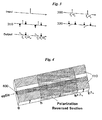
- Fig. 4 is a schematic diagram illustrating a carrier wave band modulator using a double sideband modulation method in accordance with an embodiment of the present invention.
- an electric field of light entered into a waveguide 400, E 0 (t, z) and a voltage of RF applied to a coplanar waveguide (CPW) 410, V(t, z) are defined respectively as follows.
- V t ⁇ z A ⁇ e - ⁇ c ⁇ z ⁇ sin 2 ⁇ ⁇ f c ⁇ t - ⁇ c ⁇ z
- f 0 is a frequency of a light wave entered into the waveguide 400
- f c is a frequency of RF corresponding to half of a frequency of carrier wave
- ⁇ 0 is a propagation constant of the light wave entered into the waveguide 400
- ⁇ c is a propagation constant of RF
- ⁇ c is an attenuation constant of RF.
- V eff By integrating voltage applied to the light wave while the light wave passes through one cycle region (2 ⁇ c ) including repetitively polarization reversed sections, a total effective voltage V eff is defined as follows.
- ⁇ c is c 2 ⁇ f c ⁇ n c - n 0
- k is ⁇ ⁇ c
- c is a velocity of light in a vacuum
- n c is an effective refractive index of RF
- no is an effective refractive index of light.
- V eff 4 ⁇ NA k ⁇ cos 2 ⁇ ⁇ f c ⁇ t - kh
- a phase of the total effective voltage V eff changes according to a change of starting point 'h' of polarization reverse.
- a phase difference between two total effective voltages of the two waveguides 121, 122 is ⁇ .
- phase difference between two voltages causes phase modulation of cos2 ⁇ f c t at the first waveguide 121 and phase modulation of -cos2 ⁇ f c t at the second waveguide 122 although the same voltage is applied, so as to achieve a carrier wave band modulation using a double sideband modulation method.
- Fig. 5 is a schematic diagram illustrating an intermediate frequency band modulator using a single sideband modulation method in accordance with an embodiment of the present invention.
- a voltage V (t, z) of RF applied to the third electrode part 160 is defined as follows.
- V t ⁇ z A ⁇ e - ⁇ IF ⁇ z ⁇ sin 2 ⁇ ⁇ f IF ⁇ t - ⁇ IF ⁇ z
- f IF is an intermediate frequency
- ⁇ IF is an attenuation constant of RF
- ⁇ IF is a propagation constant of RF.
- a total effective voltage V eff1 applied to a light wave while the light wave passes through the third waveguide 131 and total effective voltage V eff2 applied to a light wave while the light wave passes through the fourth waveguide 132 are defined as follows.
- ⁇ IF is c 2 ⁇ f IF ⁇ n IF - n 0
- k is ⁇ ⁇ IF
- n IF is an effective refractive index of signal with an intermediate frequency band applied.
- V eff1 and V eff2 may be simplified as follows.
- V eff ⁇ 1 2 ⁇ A k ⁇ cos 2 ⁇ ⁇ f IF ⁇ t
- V eff ⁇ 2 - 2 ⁇ A k ⁇ sin 2 ⁇ ⁇ f IF ⁇ t
- Equation 4 if half of one waveguide is polarization-reversed, a phase difference between the two total effective voltages becomes ⁇ /2. Accordingly, the above-described operation can embody intermediate frequency band modulation using a single sideband modulation method.
- a single sideband modulation is based on a principle that upper sidebands or lower sidebands of two light waves are offset through combination of the two light waves.
- two total effective voltages applied to the two waveguides 131, 132 have to have the same value.
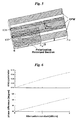
- Fig. 6 is graphs illustrating operation characteristics according to RF loss change at an intermediate frequency band modulator using a single sideband modulation method in accordance with the present invention.
- a chirp parameter ⁇ is defined as follows.
- FIG. 6 A phase difference between V eff1 and V eff2 and chirp parameter according to an attenuation constant of RF are shown in Fig. 6.
- increase in RF attenuation constant may cause increase in a chirp parameter, thereby causing distortion of characteristics of an intermediate frequency band modulator using a single sideband modulation method.
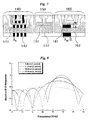
- Fig. 7 is a plan view of an integrated optical modulator in accordance with a second embodiment of the present invention.
- a SiO 2 buffer layer and electrode parts 140, 150, 160 may have a thickness of 0.3 ⁇ m and 2 ⁇ m, respectively.
- Parameters W and S are 40 ⁇ m and 60 ⁇ m, respectively. With such a structure, a calculated characteristic impedance is 40 ⁇ , an effective refractive index is 3.93, and an attenuation constant is 0.7 dB/cm.
- a frequency of carrier wave is 60 GHz
- an input frequency into a carrier wave band modulator using a double sideband modulation method is 30 GHz
- ⁇ c length of polarization reversed section
- a total modulation region is 22.4mm corresponding to four cycles of cyclical polarization.
- a length ⁇ IF of modulation region is 15.2 mm.
- Fig. 8 is graphs illustrating frequency response characteristics of a carrier wave band modulator using a double sideband modulation method according to the second embodiment of the present invention. Referring to Fig. 8, as the number of times of polarization reverse increases, a bandwidth of carrier wave is reduced.
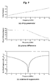
- Fig. 9 is graphs depicting operation characteristics according to a frequency at an intermediate frequency band modulator using a single sideband modulation method according to the second embodiment of the present invention.
- a chirp parameter Fig. 9 (a)
- a phase difference Fig. 9 (b)
- ratio of two sideband signals Fig. 9 (c)
- the present invention embodies an integrated optical modulator which can generate a carrier wave through polarization reverse technology and derivation of virtual RF phase change by such polarization reverse.
- the integrated optical modulator according to the present invention can produce a modulated light wave having a spectrum without influence of chromatic dispersion and perform drive by a DC bias as well as it plays a role of band modulator.
Landscapes
- Physics & Mathematics (AREA)
- Nonlinear Science (AREA)
- General Physics & Mathematics (AREA)
- Optics & Photonics (AREA)
- Electromagnetism (AREA)
- Optical Modulation, Optical Deflection, Nonlinear Optics, Optical Demodulation, Optical Logic Elements (AREA)
Abstract
A method of manufacturing the integrated optical modulator comprises the steps of preparing a ferroelectric substrate (100) comprising sections (110) whose spontaneous polarisation is either reversed (i.e. poled) or non reversed and arranged so as to induce a phase difference between modulating electric fields applied to the arms (121,122;131,132) of the Mach-Zehnder structures (180,190); forming a first optical waveguide part (120) and a second optical waveguide part (130) on the substrate; forming a buffer layer over the first and the second optical waveguide parts (120,130); forming sequentially a first electrode part (140) for applying a carrier wave modulating signal, and a second electrode part (150) for applying a DC bias signal over the first optical waveguide part (120); and forming a third electrode part (160) for applying an intermediate frequency signal over the second optical waveguide part (130).

Description
- The present invention relates to an integrated optical modulator; and, more particularly, to an integrated optical modulator including a carrier wave band modulator using a double sideband modulation method and intermediate frequency band modulator using a single sideband modulation method, which is free from chromatic dispersion.
- With an explosive increase in demand for wireless communication equipment and information, a new information communication environment is strongly required so as to transmit and receive data of more than hundreds of Mbps. Such broadband transmission necessitates a carrier wave having dozens of GHz. Particular, 60 GHz band, which is readily absorbed by oxygen, is being greatly noticed as a carrier wave in view of frequency recycling.
- There are several techniques for transmitting signals to wireless communication equipment. One technique is intermediate frequency (IF) over fiver (hereinafter referred to as "IOF') or baseband over fiber (hereinafter referred to as "BOF') which is the way that transmits data to a base station and then modulates a carrier wave with the date signal to transmit a modulated carrier wave in the base station. Another technique is radio frequency over fiber (hereinafter referred to as "ROF') which is the way that transmits a carrier wave modulated by using a data signal to a base station and then transmits directly radio frequency (RF) regenerated by a high-efficiency photodiode in the base station. Such communication to a base station is carried out by using an optical fiber with broadband and low loss characteristics. Particularly, in a circumstance requiring a large number of base stations due to short-haul, high capacity transmit/receive characteristics of a high frequency, ROF transmission is preferred because in case of the ROF method, designing a base station is relatively simple.
- In an ROF transmission system, an optical modulator to convert electric signals into optical signals is essential. To enhance transmission characteristics, various modulating methods and optical modulators corresponding to the modulating methods have been studied and developed.
- For example, a first conventional modulation method is to directly vary an RF carrier wave having dozens of GHz into an optical signal using a data signal at an optical modulator. To perform such an optical modulation, a lot of RF signals have to be processed and an optical modulator for a carrier wave band is necessary. However, in case of 60 GHz band, it is difficult to perform high efficiency optical modulation because of high RF loss and further, in case of such modulation, a transmission distance is limited due to chromatic dispersion between double sidebands.
- A second conventional modulation method is to use two light waves, wherein a frequency difference between the two light waves is the same as a frequency of carrier wave. In detail, after generation of two light waves so that a frequency difference between the two light waves is the same as a frequency of carrier wave, one light wave is transmitted without modulation, and the other light wave is modulated and transmitted by using a data signal. Then, in a receiving-end, a signal of a carrier wave band is detected by a broadband photodiode and filtered. This method ensures easier modulation compared to the above-mentioned first conventional modulation method because it requires optical modulation for only an intermediate frequency band of several GHz. However, this method has difficulty in continuously generating light waves so that a frequency difference between the light waves is the same as a frequency of carrier wave, and is vulnerable to chromatic dispersion.
- A third conventional modulation method is similar to the first conventional modulation method except that the third conventional modulation method can minimize influence of chromatic dispersion by removing one side band of a modulated signal. The third conventional modulation method is known as a single sideband (hereinafter referred to as "SSB") modulation. The SSB modulation is based on a principle that one side band is offset to be removed through the steps of dividing an RF signal having carrier wave band into two signals, conducting a 90° phase lag for one signal of them, modulating the two signals in a branched optical waveguide part of mach-zéhnder interferometer structure, respectively, and combining the modulated two light waves. However, this method also requires an optical modulator for a carrier wave band and is difficult to apply to an ROF system in spite of its advantages because of complex modulator structure and need of additional RF circuits.
- Although various modulation methods and modulators have been studied, the conventional modulation method and modulators could not be easily applied to an ROF system due to imperfect features and complex system constitution. Accordingly, there is need for a new transmission method having simple and improved characteristics and a modulator corresponding to the new transmission method.
- It is, therefore, a primary object of the present invention is to provide an optical modulator which can minimize an influence of chromatic dispersion and has relatively simple structure.
- Another object of the present invention is to provide a method for manufacturing an optical modulator which can minimize an influence of chromatic dispersion and has relatively simple structure.
- Additional advantages, objects, and features of the invention will be set forth in part in the description which follows and in part will become apparent to those having ordinary skill in the art upon examination of the following or may be learned from practice of the invention. The objectives and other advantages of the invention may be realized and attained by the structure particularly pointed out in the written description and claims hereof as well as the appended drawings.
- To achieve these objectives and other advantages and in accordance with the purpose of the invention, as embodied and broadly described herein, an integrated optical modulator comprises a carrier wave band modulator using a double sideband modulation method and an intermediate frequency band modulator using a single sideband modulation method. In another aspect, a method for manufacturing the integrated optical modulator comprises preparing a substrate having at least one polarization reversed section; forming a first optical waveguide part and second optical waveguide part on the substrate, wherein the first and second optical waveguide parts have divergence and combination structure, respectively; forming a buffer layer over the optical waveguide parts; sequentially forming a first electrode and second electrode on the first optical waveguide part; and forming a third electrode on the second optical waveguide part.
- It is to be understood that both the foregoing general description and the following detailed description of the present invention are exemplary and explanatory and are intended to provide further explanation of the invention as claimed.
- The above and other objects and features of the present invention will become apparent from the following description of preferred embodiments given in conjunction with the accompanying drawings, in which:
- Fig. 1 is a schematic diagram showing an integrated optical modulator in accordance with a first embodiment of the present invention;
- Fig. 2 is a block diagram for phase modulation by an integrated optical modulator in accordance with the present invention;
- Fig. 3 shows spectrums of light waves generated from an integrated optical modulator in accordance with the present invention;
- Fig. 4 is a schematic diagram illustrating a carrier wave band modulator using a double sideband modulation method in accordance with an embodiment of the present invention;
- Fig. 5 is a schematic diagram illustrating an intermediate frequency band modulator using a single sideband modulation method in accordance with an embodiment of the present invention;
- Fig. 6 is graphs illustrating operation characteristics according to RF loss change at an intermediate frequency band modulator using a single sideband modulation method in accordance with the present invention;
- Fig. 7 is a plan view of an integrated optical modulator in accordance with a second embodiment of the present invention;
- Fig. 8 is graphs illustrating frequency response characteristics of a carrier wave band modulator using a double sideband modulation method according to the second embodiment of the present invention; and
- Fig. 9 is graphs depicting operation characteristics according to a frequency at an intermediate frequency band modulator using a single sideband modulation method according to the second embodiment of the present invention.
- Reference will now be made in detail to the preferred embodiments of the present invention, examples of which are illustrated in the accompanying drawings.
- Fig. 1 is a schematic diagram showing an integrated optical modulator in accordance with a first embodiment of the present invention. Referring to Fig. 1, an integrated optical modulator comprises a z-cut LiNbO3 substrate 100, at least one polarization reversed
section 110 of the LiNbO3substrate 100,optical waveguide parts substrate 100, a buffer layer (not shown) formed over theoptical waveguide parts electrode parts optical waveguide parts optical waveguide parts - The
optical waveguide parts substrate 100 have a machzehnder interferometer structure zehnder interferometer structure 180 including the firstoptical waveguide part 120, afirst electrode part 140 for carrier wave band modulation and asecond electrode part 150 for applying a DC bias are formed to compose a carrier wave band optical modulator using a double sideband modulation method. - Over the second mach
zehnder interferometer structure 190 including the secondoptical waveguide part 130, athird electrode part 160 is disposed to compose an intermediate frequency band modulator using a single sideband modulation method. The second machzehnder interferometer structure 190 is connected with the first machzehnder interferometer structure 180 in series. - The first and second
optical waveguide parts center electrodes third electrode parts - Fig. 2 is a block diagram for phase modulation by an integrated optical modulator in accordance with the present invention and Fig. 3 shows spectrums of light waves generated from an integrated optical modulator in accordance with the present invention. Referring to Figs. 1 to 3, a light wave having the frequency of f0 is entered into the first
optical waveguide part 120 of the first machzehnder interferometer structure 180. - If a single frequency signal (sin2πfct) corresponding to half of a carrier wave frequency is applied to the
first electrode part 140, the same electric fields are formed at afirst waveguide 121 andsecond waveguide 122 of the first machzehnder interferometer structure 180. Since thefirst waveguide 121 andsecond waveguide 122 has a different polarization direction, respectively, they cause a refractive index change in a different direction, respectively. Therefore, phase changes of the two light waves passing through the first andsecond waveguides first waveguide 121, phase modulation of cos2πfct is performed and in thesecond waveguide 122, phase modulation of-cos2πfct is performed. - In addition, if an appropriate quantity of DC bias is applied to the
second electrode part 150, the phase difference of π is generated between the two light waves. - If the two light waves passing through the first mach
zehnder interferometer structure 180 are combined at afirst nodal point 170 after the above-described continuous phase change, the entered light wave having the frequency of f0 is converted into a light wave having two frequencies, f0-fc and f0+fc. - After passing of the first
nodal point 170, the converted light wave is entered into the secondoptical waveguide part 130 of the second machzehnder interferometer structure 190. Here, if data of intermediate frequency band is applied to thethird electrode part 160, in athird waveguide 131, phase modulation of sin2πfIFt is performed and, in afourth waveguide 132, phase modulation of cos2πfIFt is performed. - Such phase difference of 90° between two modulated signals is generated by phase velocity mismatching between light and RF, an appropriate modulation length, and definition of polarization reversed section corresponding to the modulation length.
- The above-mentioned modulation method is described in more detail referring to Figs. 4 and 5.
- A frequency spectrum at the first
nodal point 170 is shown in thereference number 300 of Fig. 3. After phase modulation in the third andfourth waveguides nodal points reference numbers nodal points nodal point 173, as shown in Fig. 3. - The light wave having the above-described frequency spectrum is transmitted to a receiving-end (not shown) and is converted into RF having frequency components of 2fc, 2fc+fIF, and 2fc-fIF through a photodiode (not shown). Here, the 2fc+fIF band or 2fc-fIF band is filtered to produce a signal having a carrier wave band to be transmitted to an antenna.
- Fig. 4 is a schematic diagram illustrating a carrier wave band modulator using a double sideband modulation method in accordance with an embodiment of the present invention. Referring to Figs. 1 and 4, an electric field of light entered into a
waveguide 400, E0(t, z) and a voltage of RF applied to a coplanar waveguide (CPW) 410, V(t, z) are defined respectively as follows. -

-

- Here, f0 is a frequency of a light wave entered into the
waveguide 400, fc is a frequency of RF corresponding to half of a frequency of carrier wave, β0 is a propagation constant of the light wave entered into thewaveguide 400, βc is a propagation constant of RF, and αc is an attenuation constant of RF. - By integrating voltage applied to the light wave while the light wave passes through one cycle region (2Λc) including repetitively polarization reversed sections, a total effective voltage Veff is defined as follows.
-


- Here, Λc is


- If there is no RF loss during passing of
CPW 410 and a total modulation length L is 2N · A, the total effective voltage Veff is simplified as follows. -

- Referring to Equation 4, a phase of the total effective voltage Veff changes according to a change of starting point 'h' of polarization reverse. When starting points of polarization reverse in the two
waveguides zehnder interferometer structure 180 are h1 and h2, respectively, and it is (h1-h2) = Λ, a phase difference between two total effective voltages of the twowaveguides - Therefore, such a phase difference between two voltages causes phase modulation of cos2πfct at the
first waveguide 121 and phase modulation of -cos2πfct at thesecond waveguide 122 although the same voltage is applied, so as to achieve a carrier wave band modulation using a double sideband modulation method. - Fig. 5 is a schematic diagram illustrating an intermediate frequency band modulator using a single sideband modulation method in accordance with an embodiment of the present invention. Referring to Fig. 1 and Fig. 5, a voltage V (t, z) of RF applied to the
third electrode part 160 is defined as follows. -

- Here, fIF is an intermediate frequency, αIF is an attenuation constant of RF, and βIF is a propagation constant of RF.
- A total effective voltage Veff1 applied to a light wave while the light wave passes through the
third waveguide 131 and total effective voltage Veff2 applied to a light wave while the light wave passes through thefourth waveguide 132 are defined as follows. -


-
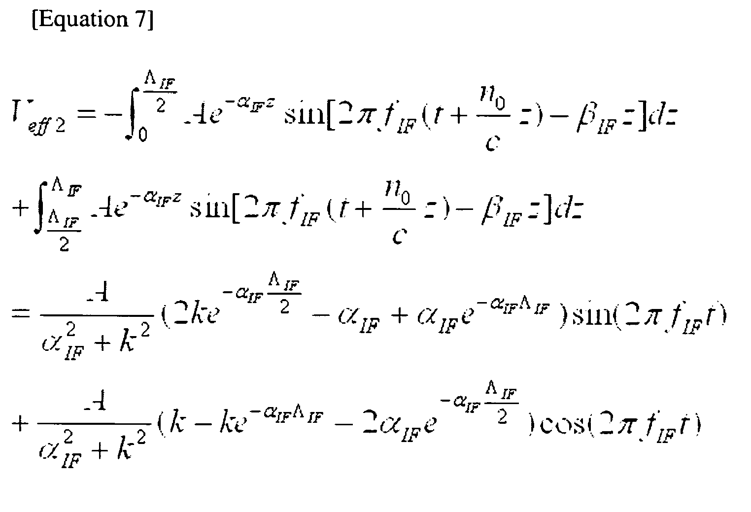
- Here, ΛIF is


- If the
third electrode part 160 is no loss electrode, Veff1 and Veff2 may be simplified as follows. -

-

- In Equation 4, if half of one waveguide is polarization-reversed, a phase difference between the two total effective voltages becomes π/2. Accordingly, the above-described operation can embody intermediate frequency band modulation using a single sideband modulation method.
- In addition, if aside from RF a separate DC bias is applied to the
third electrode part 130, a light wave passing through thefourth waveguide 132 half of which is polarization-reversed is not influenced by the DC bias, but a light wave passing through thethird waveguide 131 is delayed by the DC bias. Generally, such an operation to delay a light wave is impossible at a band modulator having repetitively polarization reversed sections and, therefore, in order to embody such an operation an additional electrode for driving a DC bias has to be inserted. The insertion of additional electrode requires an additional space, thereby obstructing integration. Such a problem, however, can be solved by a structure according to the present invention. - A single sideband modulation is based on a principle that upper sidebands or lower sidebands of two light waves are offset through combination of the two light waves. Thus, to improve modulation efficiency, two total effective voltages applied to the two
waveguides - However, in an intermediate frequency band modulator using a single sideband modulation method, as an attenuation constant of RF increases, a difference between two effective voltages is generated, thereby causing deterioration of modulation characteristics.
- Fig. 6 is graphs illustrating operation characteristics according to RF loss change at an intermediate frequency band modulator using a single sideband modulation method in accordance with the present invention. A chirp parameter η is defined as follows.
-

- A phase difference between Veff1 and Veff2 and chirp parameter according to an attenuation constant of RF are shown in Fig. 6. Referring to Fig. 6, increase in RF attenuation constant may cause increase in a chirp parameter, thereby causing distortion of characteristics of an intermediate frequency band modulator using a single sideband modulation method.
- Fig. 7 is a plan view of an integrated optical modulator in accordance with a second embodiment of the present invention. Referring to Fig. 7, a SiO2 buffer layer and
electrode parts - Fig. 8 is graphs illustrating frequency response characteristics of a carrier wave band modulator using a double sideband modulation method according to the second embodiment of the present invention. Referring to Fig. 8, as the number of times of polarization reverse increases, a bandwidth of carrier wave is reduced.
- Fig. 9 is graphs depicting operation characteristics according to a frequency at an intermediate frequency band modulator using a single sideband modulation method according to the second embodiment of the present invention. Referring to Fig. 9, in a 5.5 GHz intermediate frequency band modulator, a chirp parameter (Fig. 9 (a)), a phase difference (Fig. 9 (b)), and ratio of two sideband signals (Fig. 9 (c)) according to a frequency are calculated and graphed.
- Accordingly, by connecting a carrier wave band modulator using a double sideband modulation method and an intermediate frequency band modulator using a single sideband modulation method in series, the present invention embodies an integrated optical modulator which can generate a carrier wave through polarization reverse technology and derivation of virtual RF phase change by such polarization reverse.
- In addition, the integrated optical modulator according to the present invention can produce a modulated light wave having a spectrum without influence of chromatic dispersion and perform drive by a DC bias as well as it plays a role of band modulator.
- It is noted that this patent claims priority from
Korean Patent Application Serial Number 10-2005-0074320, which was filed on August 12, 2005 - Although certain example methods, apparatus and articles of manufacture have been described herein, the scope of coverage of this invention is not limited thereto. On the contrary, this patent covers all methods, apparatus and articles of manufacture fairly falling within the scope of the appended claims either literally or under the doctrine of equivalents.
Claims (15)
- An integrated optical modulator comprising a carrier wave band modulator using a double sideband modulation method and an intermediate frequency band modulator using a single sideband modulation method, wherein the carrier wave band modulator and intermediate frequency band modulator are connected in series.
- The integrated optical modulator as defined by claim 1, wherein the carrier wave band modulator using a double sideband modulation method comprises:a substrate having cyclically polarization reversed sections;a first optical waveguide part disposed on the substrate, the first optical waveguide part comprising a first waveguide and a second waveguide, the first optical waveguide part being formed by combination and divergence of the first and second waveguides; anda first electrode part and a second electrode part formed over the first optical waveguide part.
- The integrated optical modulator as defined by claim 2, wherein the first waveguide and the second waveguide have a different polarization direction each other.
- The integrated optical modulator as defined by claim 2, wherein the first electrode part receives a single frequency signal corresponding to half of a frequency of carrier wave and the second electrode part receives a DC bias, so as to perform a carrier wave band modulation using a double sideband modulation method.
- The integrated optical modulator as defined by claim 1, wherein the intermediate frequency band modulator using a single sideband modulation method comprises:a substrate having a polarization reversed section;a second optical waveguide part disposed on the substrate, the second optical waveguide part comprising a third waveguide and a fourth waveguide, the second optical waveguide part being formed by combination and divergence of the third and fourth waveguides; anda third electrode part disposed over the second optical waveguide part.
- The integrated optical modulator as defined by claim 5, wherein the fourth waveguide includes a polarization reversed section taking up half the fourth waveguide.
- The integrated optical modulator as defined by claim 5, wherein the third electrode part receives data having an intermediate frequency band so as to perform intermediate frequency band modulation using a single sideband modulation method.
- The integrated optical modulator as defined by claim 5, wherein the third electrode part receives a DC bias so as to delay a light wave passing through the third waveguide.
- A method for manufacturing an integrated optical modulator comprising:preparing a substrate having at least one polarization reversed section;forming a first optical waveguide part and a second optical waveguide part on the substrate, wherein the first and second optical waveguide parts have combination and divergence structure, respectively;forming a buffer layer over the first and second optical waveguide parts;forming sequentially a first electrode part and a second electrode part over the first optical waveguide part; andforming a third electrode part over the second optical waveguide part.
- The method as defined by claim 9, wherein the first optical waveguide part and the second optical waveguide part are connected in series.
- The method as defined by claim 9, wherein the first optical waveguide part comprises a first waveguide and a second waveguide wherein the first waveguide has a different polarization direction from the second waveguide.
- The method as defined by claim 9, wherein the second optical waveguide part comprises a third waveguide and a fourth waveguide wherein the fourth waveguide includes a polarization reversed section taking up half the fourth waveguide.
- The method as defined by claim 9, wherein the first electrode part is used for carrier wave band modulation.
- The method as defined by claim 9, wherein the second electrode part receives a DC bias.
- The method as defined by claim 9, wherein the third electrode part is used for intermediate frequency band modulation.
Applications Claiming Priority (1)
| Application Number | Priority Date | Filing Date | Title |
|---|---|---|---|
| KR1020050074320A KR100688072B1 (en) | 2005-08-12 | 2005-08-12 | Integrated optical modulator and its manufacturing method |
Publications (1)
| Publication Number | Publication Date |
|---|---|
| EP1752821A1 true EP1752821A1 (en) | 2007-02-14 |
Family
ID=36603638
Family Applications (1)
| Application Number | Title | Priority Date | Filing Date |
|---|---|---|---|
| EP05028328A Withdrawn EP1752821A1 (en) | 2005-08-12 | 2005-12-23 | Integrated optical modulator and method for manufacturing the same |
Country Status (4)
| Country | Link |
|---|---|
| US (1) | US7440642B2 (en) |
| EP (1) | EP1752821A1 (en) |
| JP (1) | JP4980620B2 (en) |
| KR (1) | KR100688072B1 (en) |
Families Citing this family (6)
| Publication number | Priority date | Publication date | Assignee | Title |
|---|---|---|---|---|
| KR100819308B1 (en) * | 2005-09-02 | 2008-04-03 | 삼성전자주식회사 | ROPE link device to enable stable TD system wireless service |
| CN101501555B (en) * | 2006-06-14 | 2012-10-24 | 安立股份有限公司 | Optical modulator |
| JP5055947B2 (en) * | 2006-10-20 | 2012-10-24 | 富士通オプティカルコンポーネンツ株式会社 | Optical modulator and transmitter |
| KR100860415B1 (en) * | 2006-12-01 | 2008-09-26 | 한국전자통신연구원 | Optical modulator, method and Apparatus for controlling bias voltage thereof |
| JP4982861B2 (en) * | 2007-08-29 | 2012-07-25 | 国立大学法人大阪大学 | Radio signal receiving and separating device |
| JP5594192B2 (en) * | 2011-03-08 | 2014-09-24 | 住友大阪セメント株式会社 | Light modulator |
Citations (1)
| Publication number | Priority date | Publication date | Assignee | Title |
|---|---|---|---|---|
| JP2002062516A (en) * | 2000-08-22 | 2002-02-28 | Japan Science & Technology Corp | Periodic domain inversion structure electro-optic SSB optical modulator / optical frequency shifter |
Family Cites Families (11)
| Publication number | Priority date | Publication date | Assignee | Title |
|---|---|---|---|---|
| US1666206A (en) * | 1925-01-15 | 1928-04-17 | Western Electric Co | Modulation system |
| US5278924A (en) * | 1993-02-04 | 1994-01-11 | Hughes Aircraft Company | Periodic domain reversal electro-optic modulator |
| US5526158A (en) * | 1994-12-22 | 1996-06-11 | Trw Inc. | Low-bias heterodyne fiber-optic communication link |
| JP3532866B2 (en) * | 2001-02-15 | 2004-05-31 | 東京通信機工業株式会社 | Single sideband suppressed optical modulated wave generator |
| US6501867B2 (en) * | 2001-04-17 | 2002-12-31 | Lucent Technologies Inc. | Chirp compensated Mach-Zehnder electro-optic modulator |
| KR100438891B1 (en) * | 2001-12-20 | 2004-07-02 | 한국전자통신연구원 | Semiconductor optical modulator |
| JP4362622B2 (en) * | 2002-09-20 | 2009-11-11 | 財団法人大阪産業振興機構 | Optical frequency shift method and optical frequency shifter |
| KR100493095B1 (en) * | 2002-10-16 | 2005-06-02 | 삼성전자주식회사 | Optical transmitting system |
| WO2004053574A1 (en) * | 2002-12-06 | 2004-06-24 | Fujitsu Limited | Optical modulator |
| KR100539893B1 (en) * | 2003-11-12 | 2005-12-28 | 삼성전자주식회사 | Optical transmitter for dense wavelength division multiplexing |
| JP4429711B2 (en) * | 2003-12-17 | 2010-03-10 | 富士通株式会社 | Light modulator |
-
2005
- 2005-08-12 KR KR1020050074320A patent/KR100688072B1/en not_active Expired - Fee Related
- 2005-12-15 US US11/304,031 patent/US7440642B2/en not_active Expired - Fee Related
- 2005-12-23 EP EP05028328A patent/EP1752821A1/en not_active Withdrawn
- 2005-12-28 JP JP2005377502A patent/JP4980620B2/en not_active Expired - Fee Related
Patent Citations (1)
| Publication number | Priority date | Publication date | Assignee | Title |
|---|---|---|---|---|
| JP2002062516A (en) * | 2000-08-22 | 2002-02-28 | Japan Science & Technology Corp | Periodic domain inversion structure electro-optic SSB optical modulator / optical frequency shifter |
Non-Patent Citations (7)
| Title |
|---|
| FUSTER J M ET AL: "Analysis of hybrid modulation techniques in MZ-EOM-based photonic mixers to overcome dispersion-induced power penalty in up-converting millimeter-wave fiber-optic links", MICROWAVE AND OPTICAL TECHNOLOGY LETTERS WILEY USA, vol. 23, no. 2, 20 October 1999 (1999-10-20), pages 127 - 129, XP009068756, ISSN: 0895-2477 * |
| GRAHAM H SMITH ET AL: "Overcoming Chromatic-Dispersion Effects in Fiber-Wireless Systems Incorporating External Modulators", IEEE TRANSACTIONS ON MICROWAVE THEORY AND TECHNIQUES, IEEE SERVICE CENTER, PISCATAWAY, NJ, US, vol. 45, no. 8, August 1997 (1997-08-01), pages 1410 - 1415, XP011036928, ISSN: 0018-9480 * |
| J. L. CORRAL ET AL.: "General Expressions for IM/DD Dispersive Analog Optical Links With External Modulation or Optical Up-Conversion in a Mach-Zehnder Electrooptical Modulator", IEEE TRANS. ON MTT, vol. 49, no. 10, October 2001 (2001-10-01), pages 1968 - 1976, XP011038423 * |
| JEEHOON HAN ET AL: "Reduction of fiber chromatic dispersion effects in fiber-wireless and photonic time-stretching system using polymer modulators", JOURNAL OF LIGHTWAVE TECHNOLOGY IEEE USA, vol. 21, no. 6, June 2003 (2003-06-01), pages 1504 - 1509, XP002388768, ISSN: 0733-8724 * |
| MURATA H ET AL: "Optical single-sideband modulation by using periodically domain-inverted LiTaO3 guided-wave modulators", MICROWAVE PHOTONICS, 2002. INTERNATIONAL TOPICAL MEETING ON NOV 5-8, 2002, PISCATAWAY, NJ, USA,IEEE, 5 November 2002 (2002-11-05), pages 53 - 56, XP010623119, ISBN: 4-88552-187-4 * |
| PATENT ABSTRACTS OF JAPAN vol. 2002, no. 06 4 June 2002 (2002-06-04) * |
| R. MONTGOMERY AND R. DESALVO: "A Novel Technique for Double Sideband Suppressed Carrier Modulation of Optical Fields", IEEE PHOTONICS TECHNOLOGY LETTERS, vol. 7, no. 4, April 1995 (1995-04-01), pages 434 - 436 * |
Also Published As
| Publication number | Publication date |
|---|---|
| JP2007052393A (en) | 2007-03-01 |
| KR100688072B1 (en) | 2007-03-02 |
| JP4980620B2 (en) | 2012-07-18 |
| KR20070019390A (en) | 2007-02-15 |
| US7440642B2 (en) | 2008-10-21 |
| US20070036478A1 (en) | 2007-02-15 |
Similar Documents
| Publication | Publication Date | Title |
|---|---|---|
| JP4092378B2 (en) | Optical millimeter-wave / microwave signal generation method and apparatus | |
| US5644664A (en) | Fiber optic digital transmission system | |
| CN102681216B (en) | Light control element | |
| CN104022830B (en) | A Device for Generating Octave-Frequency Millimeter Waves Using a Mach-Zehnder Modulator | |
| EP1995633A1 (en) | Super flat optical frequency com signal generator | |
| CN101777953B (en) | Light double-sideband modulation device and method for transmitting two paths of signals | |
| US6504640B2 (en) | Resonant optical modulators with zero chirp | |
| US7555223B2 (en) | UWB signal generator using optical FSK modulator | |
| JPH03203716A (en) | Electrooptical modulator | |
| WO2009096170A1 (en) | Super flat optical frequency comb signal generator | |
| CN103078680A (en) | Quadruplicated frequency millimeter wave generation method based on double-parallel MZ (Mach-zehnder) modulator | |
| EP2355377A1 (en) | Optical modulation device and optical modulation method | |
| US7660027B2 (en) | Optical modulator and modulation method | |
| US8755641B2 (en) | Optical modulator | |
| EP1921485B1 (en) | Optical amplitude modulating system capable of removing high-order component | |
| US7440642B2 (en) | Integrated optical modulator and method for manufacturing the same | |
| JPH02269309A (en) | Optical modulating system | |
| US8311415B2 (en) | Frequency up-conversion system and method for the same | |
| CN107733530B (en) | Simplified device and method for generating polarization insensitive high-frequency-multiplication optical carrier millimeter wave | |
| Pandey et al. | Broadly tunable wideband optical single sideband generation using self-coupled silicon resonator | |
| JP2002062516A (en) | Periodic domain inversion structure electro-optic SSB optical modulator / optical frequency shifter | |
| Arya et al. | Performance improved tunable millimeter‐wave signal generation employing UFBG based AOTF with bit walk‐off effect compensation | |
| Yamaguchi et al. | Highly Efficient Thin-Film Lithium Niobate Modulator with Resonant-Type Electrode | |
| JP4197316B2 (en) | Light modulator | |
| Cui et al. | Mechanism for 32-FOLD Frequency Multiplication Terahertz Wave Generation Based on Two Dual-Parallel and One Cascaded Mzms Without Filtering for High-Frequency Communications |
Legal Events
| Date | Code | Title | Description |
|---|---|---|---|
| PUAI | Public reference made under article 153(3) epc to a published international application that has entered the european phase |
Free format text: ORIGINAL CODE: 0009012 |
|
| AK | Designated contracting states |
Kind code of ref document: A1 Designated state(s): AT BE BG CH CY CZ DE DK EE ES FI FR GB GR HU IE IS IT LI LT LU LV MC NL PL PT RO SE SI SK TR |
|
| AX | Request for extension of the european patent |
Extension state: AL BA HR MK YU |
|
| 17P | Request for examination filed |
Effective date: 20070629 |
|
| 17Q | First examination report despatched |
Effective date: 20070802 |
|
| AKX | Designation fees paid |
Designated state(s): AT BE BG CH CY CZ DE DK EE ES FI FR GB GR HU IE IS IT LI LT LU LV MC NL PL PT RO SE SI SK TR |
|
| STAA | Information on the status of an ep patent application or granted ep patent |
Free format text: STATUS: THE APPLICATION IS DEEMED TO BE WITHDRAWN |
|
| 18D | Application deemed to be withdrawn |
Effective date: 20080829 |