EP1750490A1 - Cooling of an electronic power device - Google Patents
Cooling of an electronic power device Download PDFInfo
- Publication number
- EP1750490A1 EP1750490A1 EP05291651A EP05291651A EP1750490A1 EP 1750490 A1 EP1750490 A1 EP 1750490A1 EP 05291651 A EP05291651 A EP 05291651A EP 05291651 A EP05291651 A EP 05291651A EP 1750490 A1 EP1750490 A1 EP 1750490A1
- Authority
- EP
- European Patent Office
- Prior art keywords
- arrangement
- power device
- pcb
- metal
- cooling
- Prior art date
- Legal status (The legal status is an assumption and is not a legal conclusion. Google has not performed a legal analysis and makes no representation as to the accuracy of the status listed.)
- Granted
Links
Images


Classifications
-
- H—ELECTRICITY
- H05—ELECTRIC TECHNIQUES NOT OTHERWISE PROVIDED FOR
- H05K—PRINTED CIRCUITS; CASINGS OR CONSTRUCTIONAL DETAILS OF ELECTRIC APPARATUS; MANUFACTURE OF ASSEMBLAGES OF ELECTRICAL COMPONENTS
- H05K1/00—Printed circuits
- H05K1/02—Details
- H05K1/0201—Thermal arrangements, e.g. for cooling, heating or preventing overheating
- H05K1/0203—Cooling of mounted components
- H05K1/0209—External configuration of printed circuit board adapted for heat dissipation, e.g. lay-out of conductors, coatings
-
- H—ELECTRICITY
- H05—ELECTRIC TECHNIQUES NOT OTHERWISE PROVIDED FOR
- H05K—PRINTED CIRCUITS; CASINGS OR CONSTRUCTIONAL DETAILS OF ELECTRIC APPARATUS; MANUFACTURE OF ASSEMBLAGES OF ELECTRICAL COMPONENTS
- H05K1/00—Printed circuits
- H05K1/18—Printed circuits structurally associated with non-printed electric components
- H05K1/189—Printed circuits structurally associated with non-printed electric components characterised by the use of flexible or folded printed circuits
-
- H—ELECTRICITY
- H05—ELECTRIC TECHNIQUES NOT OTHERWISE PROVIDED FOR
- H05K—PRINTED CIRCUITS; CASINGS OR CONSTRUCTIONAL DETAILS OF ELECTRIC APPARATUS; MANUFACTURE OF ASSEMBLAGES OF ELECTRICAL COMPONENTS
- H05K2201/00—Indexing scheme relating to printed circuits covered by H05K1/00
- H05K2201/09—Shape and layout
- H05K2201/09209—Shape and layout details of conductors
- H05K2201/09654—Shape and layout details of conductors covering at least two types of conductors provided for in H05K2201/09218 - H05K2201/095
- H05K2201/09781—Dummy conductors, i.e. not used for normal transport of current; Dummy electrodes of components
-
- H—ELECTRICITY
- H05—ELECTRIC TECHNIQUES NOT OTHERWISE PROVIDED FOR
- H05K—PRINTED CIRCUITS; CASINGS OR CONSTRUCTIONAL DETAILS OF ELECTRIC APPARATUS; MANUFACTURE OF ASSEMBLAGES OF ELECTRICAL COMPONENTS
- H05K2201/00—Indexing scheme relating to printed circuits covered by H05K1/00
- H05K2201/10—Details of components or other objects attached to or integrated in a printed circuit board
- H05K2201/10007—Types of components
- H05K2201/10166—Transistor
-
- H—ELECTRICITY
- H05—ELECTRIC TECHNIQUES NOT OTHERWISE PROVIDED FOR
- H05K—PRINTED CIRCUITS; CASINGS OR CONSTRUCTIONAL DETAILS OF ELECTRIC APPARATUS; MANUFACTURE OF ASSEMBLAGES OF ELECTRICAL COMPONENTS
- H05K2201/00—Indexing scheme relating to printed circuits covered by H05K1/00
- H05K2201/10—Details of components or other objects attached to or integrated in a printed circuit board
- H05K2201/10431—Details of mounted components
- H05K2201/10439—Position of a single component
- H05K2201/10454—Vertically mounted
-
- H—ELECTRICITY
- H05—ELECTRIC TECHNIQUES NOT OTHERWISE PROVIDED FOR
- H05K—PRINTED CIRCUITS; CASINGS OR CONSTRUCTIONAL DETAILS OF ELECTRIC APPARATUS; MANUFACTURE OF ASSEMBLAGES OF ELECTRICAL COMPONENTS
- H05K2201/00—Indexing scheme relating to printed circuits covered by H05K1/00
- H05K2201/10—Details of components or other objects attached to or integrated in a printed circuit board
- H05K2201/10431—Details of mounted components
- H05K2201/10507—Involving several components
- H05K2201/10522—Adjacent components
-
- H—ELECTRICITY
- H05—ELECTRIC TECHNIQUES NOT OTHERWISE PROVIDED FOR
- H05K—PRINTED CIRCUITS; CASINGS OR CONSTRUCTIONAL DETAILS OF ELECTRIC APPARATUS; MANUFACTURE OF ASSEMBLAGES OF ELECTRICAL COMPONENTS
- H05K2201/00—Indexing scheme relating to printed circuits covered by H05K1/00
- H05K2201/10—Details of components or other objects attached to or integrated in a printed circuit board
- H05K2201/10613—Details of electrical connections of non-printed components, e.g. special leads
- H05K2201/10954—Other details of electrical connections
- H05K2201/10969—Metallic case or integral heatsink of component electrically connected to a pad on PCB
-
- H—ELECTRICITY
- H05—ELECTRIC TECHNIQUES NOT OTHERWISE PROVIDED FOR
- H05K—PRINTED CIRCUITS; CASINGS OR CONSTRUCTIONAL DETAILS OF ELECTRIC APPARATUS; MANUFACTURE OF ASSEMBLAGES OF ELECTRICAL COMPONENTS
- H05K3/00—Apparatus or processes for manufacturing printed circuits
- H05K3/30—Assembling printed circuits with electric components, e.g. with resistors
- H05K3/32—Assembling printed circuits with electric components, e.g. with resistors electrically connecting electric components or wires to printed circuits
- H05K3/34—Assembling printed circuits with electric components, e.g. with resistors electrically connecting electric components or wires to printed circuits by soldering
- H05K3/341—Surface mounted components
Definitions
- the invention relates to an arrangement comprising at least one electronic power device, in particular a power transistor, and means for cooling the at least one power device, wherein the means comprise a separate metal face for each power device.
- a typical cooling comprises a massive aluminium metal cooler glued or clamped onto the device to be cooled.
- a thin electrically isolating heat conductor foil is arranged between the power device and the metal cooler.
- a heat spreader comprises a copper foil sandwiched between electrically insulating films.
- the heat spreader is glued onto the device to be cooled, such as a chip or an IC (integrated circuit) device, with a pressure sensitive adhesive.
- the metal face is soldered to the respective power device.
- the installation by soldering offers a strong, durable and highly reliable kind of fixing of the metal face.
- the metal face is linked to the power device to be cooled with a low thermal resistance.
- the metal face is preferably a laminar piece of metal, but may also be comprised in a more complex or even massive metal component.
- the metal face distributes the heat over a large surface area, and the heat may be taken away by air convection and, at higher temperatures, by heat radiation. If desired, the metal face may be linked to further cooling components in order to increase the cooling effect within the total arrangement.
- the metal of the metal face must be solderable, such as copper or brass.
- Typical electronic power devices to be cooled in accordance with the invention are devices that can be mounted on a PCB and include in particular MOSFETs, high power bipolar transistors and voltage regulators.
- the metal face comprises a piece of sheet metal, in particular a piece of copper sheet metal.
- a piece of sheet metal is easy to handle and in particular suited for a separate cooling of a single electronic power device.
- the arrangement comprises a multitude of power devices.
- PCB printed circuit board
- the PCB is flexible. By this means, non-linearly arranged power devices can be provided with a common PCB for cooling purposes. During production of the arrangement, the PCB can be held flat, but in use, the PCB can be bent corresponding to the desired power device positions.
- the latter can be further developed in that the separate metal faces are arranged in series, and that neighbouring metal faces interdigitate, in particular with interdigitating meanders.
- the edges of the metal faces are not straight, but are contorted, with the neighbouring edges separated a little but corresponding to each other.
- the metal of the metal faces strengthens the PCB material, so a straight bend along the edges (which probably would cause the PCB to break) in the PCB will not occur. Instead, the bend will follow the gap between the interdigitating edge lines, what is less straining for the PCB material.
- inexpensive standard FR4 material can be used for the PCB at sufficient flexibility.
- Particularly preferred are wavelike edge contours.
- the PCB comprises a thin electrically isolating foil. On the sides of this foil, the metal faces and the continuous metal surface area may be arranged.
- the foil prevents electrical short circuits, but only has minimal thermal resistance, so heat may be spread all over the metal surface area efficiently.
- the PCB comprises a thin, non-metallic lacquering, in particular a solder-stopping lacquering, on at least part of the first and/or second side.
- the lacquering improves the heat radiation of metal surfaces, in particular at higher temperatures.
- the lacquering is not applied at surfaces intended for soldering.
- the inventive method is an inexpensive and easy to automate way to produce inventive arrangements.
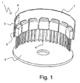
- Fig. 1 shows an inventive arrangement 1 installed on a circular electronic 2, which is, for example, part of an electric motor.
- the arrangement 1 comprises seven power devices 3, which are here MOSFETs. Their electric contacts 4 are soldered into the circular electronic 2.
- PCB printed circuit board
- the metal faces 6 are attached to an electrically isolating layer of the PCB 7. Only one metal face 6 is shown in detail in Fig. 1 for simplification.
- the outer, second side of the PCB 7, is almost completely covered with a continuous metal surface area (not shown in Fig. 1) which improves the cooling effect of the PCB 7.
- Fig. 2a shows the arrangement 1 before installation, i.e. in a flat arrangement of the power devices 3 one after another.
- the cooling tab 5 which is basically a piece of copper thermally linking the interior of the power device 3 with the surrounding for cooling purposes.
- Each cooling tab 5 typically is, in use, subject to a different voltage, so the cooling tabs 5 need to be electrically isolated. Therefore, the metal faces 6, to which the cooling tabs 5 are soldered to, are separated from neighboring metal faces 6 by a small gap. Only one metal face 6 is shown for simplification again.
- Figs. 2b, 2c show the arrangement of Fig. 2a in top view and in side view.
- Fig. 3a shows another inventive arrangement 31, comprising a single power device 3 with a cooling tab 5.
- the cooling tab 5 of the power device 3 is directly soldered onto a piece of sheet metal 32 made of copper.
- the arrangement 31 may be mounted on a piece of electronic.
- Figs. 3b, 3c show the arrangement of Fig. 3a in top view and side view, respectively.
- Figs. 4 and 5a through 5e detail the design of an inventive arrangement 41 which comprises eight power devices 3 (numbered F1 through F8) and a PCB 7, what is shown in Fig. 4.
- the PCB 7 comprises several layers of different materials, which are detailed in Figs. 5a through 5e.
- the basic component of the PCB 7 is a layer of electrically isolating material 51, whose edge is shown as the outer edge of the PCB in Fig. 5a.
- this electrically isolating layer 51 is made of standard FR4 PCB material. Its thickness is about 0.2 mm.
- Such layers are typically used for multiplayer PCBs, but may be applied here directly, wherein its thin thickness grants flexibility.
- the copper layer On top of this electrically isolating layer 51, there is a copper layer provided, what is shown as black areas in Fig. 5a.
- the thickness of the copper layer is about 70 ⁇ m.
- the copper layer comprises eight metal faces 52, which are arranged in series. The edges 53 of neighboring metal faces 52 interdigitate with fingers in the shape of meanders.
- the gap between neighboring metal faces 52 is curved s-shaped, so a sharp, straight bend of the PCB may not occur. This lessens the probability of a break in such an area. An evenly round curvature of the gap is preferred in this context.
- the gaps provide electrical isolation of the metal faces 52.
- solder-stopping lacquering 54 On top of the copper layer of Fig. 5a, there is a layer of solder-stopping lacquering 54, as shown in black in Fig. 5b. The areas free of solder stopping lacquering are intended for soldering the cooling tabs of the power devices (see Fig. 4). The solder-stopping lacquering improves the heat radiation of the underlying copper layer (see Fig. 5a).
- the solder-stopping lacquering has a thickness of about 20 ⁇ m.
- soldering paste 55 is also on top of the copper layer of Fig. 5a.
- the areas of soldering paste 55 correspond to the areas where no solder-stopping lacquering has been applied (see Fig. 5b).
- the continuous metal surface area is a thin copper layer of about 70 ⁇ m thickness, which thermally short-circuits the separate metal faces of the top copper layer. It also improves the cooling effect of the total arrangement enormously.
- the continuous metal surface area (compare Fig. 5d) is sealed with a thin layer of solder-stopping lacquering 57, which is shown in black in Fig. 5e.
- the solder-stopping lacquering which has a thickness of typically 20 ⁇ m, improves the heat radiation of the covered copper material of the continuous metal surface area.
- Figs. 4, 5a-5e may be produced on one large PCB sheet in parallel, wherein the separate arrangements are detached after completing the production of the PCB sheet.
- Typical PCB sheets comprise sixteen inventive arrangements, each of which comprises for example eight power devices.
- an SMD reflow procedure may be applied in accordance with the invention.
- the power devices orient automatically with the aid of capillary forces and interfacial energies, what simplifies the production compared to conventional techniques using masks for component orientation. Note that different from the state of the art, the power devices are not oriented with the aid of the metal surfaces of their electric contacts (“legs"), but with the metal surfaces of their cooling tabs, which are located at a side face of the power devices.
- Ssimilar production techniques may be applied with a single pieces of sheet metal soldered to one power device each, as described in Figs. 3a-3c, wherein a sheet of sheet metal replaces the PCB sheet, and the inventive arrangements are punched out of the sheet of sheet metal.
- the electronic power devices are cooled sufficiently to overcome limitations of not cooled power devices.
- the additional costs are low, in particular compared with known cooling techniques.
Landscapes
- Engineering & Computer Science (AREA)
- Microelectronics & Electronic Packaging (AREA)
- Cooling Or The Like Of Electrical Apparatus (AREA)
- Cooling Or The Like Of Semiconductors Or Solid State Devices (AREA)
- Power Conversion In General (AREA)
- Rectifiers (AREA)
Abstract
Description
- The invention relates to an arrangement comprising at least one electronic power device, in particular a power transistor, and means for cooling the at least one power device, wherein the means comprise a separate metal face for each power device.
- Such an arrangement is disclosed in the commercial publication "Thermal Management Products" of Chomerics, Woburn, MA, USA, October 1999.
- In electronic power devices, such as power transistors, heat is produced. Uncooled power devices require a sharp current limitation in order to work properly. When the power devices are used in an electric motor, for example, the current limitation also deteriorates the dynamics and the capacity of the electric motor.
- In order to avoid such limitations, it is known to install a cooling onto the power devices. A typical cooling comprises a massive aluminium metal cooler glued or clamped onto the device to be cooled. For electrical isolation, a thin electrically isolating heat conductor foil is arranged between the power device and the metal cooler.
- In the commercial publication of Chomerics, heat spreaders are described. A heat spreader comprises a copper foil sandwiched between electrically insulating films. The heat spreader is glued onto the device to be cooled, such as a chip or an IC (integrated circuit) device, with a pressure sensitive adhesive.
- The coolings of the state of the art are laborious and expensive to install, since the installation requires manual work. Often the adhesion is inadequate, e.g. due to installation errors, or the adhesion deteriorates over time, leading to a poor cooling effect only.
- It is therefore the object of the invention to provide a cooling for an electronic power device that is simple and inexpensive to install, and which offers a sufficient and reliable cooling capacity.
- This object is achieved, in accordance with the invention, by an arrangement as described in the beginning, characterized in that the metal face is soldered to the respective power device. The installation by soldering offers a strong, durable and highly reliable kind of fixing of the metal face. The metal face is linked to the power device to be cooled with a low thermal resistance. The metal face is preferably a laminar piece of metal, but may also be comprised in a more complex or even massive metal component. The metal face distributes the heat over a large surface area, and the heat may be taken away by air convection and, at higher temperatures, by heat radiation. If desired, the metal face may be linked to further cooling components in order to increase the cooling effect within the total arrangement. The metal of the metal face must be solderable, such as copper or brass. The soldering can be automated easily, similar to mounting of a PCB, so that the installation costs can be reduced in series production. Typical electronic power devices to be cooled in accordance with the invention are devices that can be mounted on a PCB and include in particular MOSFETs, high power bipolar transistors and voltage regulators.
- In a preferred embodiment of the inventive arrangement, the metal face comprises a piece of sheet metal, in particular a piece of copper sheet metal. A piece of sheet metal is easy to handle and in particular suited for a separate cooling of a single electronic power device.
- Further preferred is an embodiment, wherein the arrangement comprises a multitude of power devices. The more power devices to be cooled, the more costs can be saved with the invention. Since the metal faces of each power device are separate, they can be kept electrically isolated from each other.
- A highly preferred further development of this embodiment is characterized in that the means comprise a printed circuit board (=PCB),
that the PCB comprises a first side with the metal faces, with each power device soldered to one separate metal face,
and that the PCB comprises a second side with a continuous metal surface area. The use of a PCB allows to standardize and automate the installation of cooling means in accordance with the invention, i.e. the production of arrangements in accordance with the invention. - In further development of this, the PCB is flexible. By this means, non-linearly arranged power devices can be provided with a common PCB for cooling purposes. During production of the arrangement, the PCB can be held flat, but in use, the PCB can be bent corresponding to the desired power device positions.
- The latter can be further developed in that the separate metal faces are arranged in series, and that neighbouring metal faces interdigitate, in particular with interdigitating meanders. In other words, the edges of the metal faces are not straight, but are contorted, with the neighbouring edges separated a little but corresponding to each other. The metal of the metal faces strengthens the PCB material, so a straight bend along the edges (which probably would cause the PCB to break) in the PCB will not occur. Instead, the bend will follow the gap between the interdigitating edge lines, what is less straining for the PCB material. By this means, even inexpensive standard FR4 material can be used for the PCB at sufficient flexibility. Particularly preferred are wavelike edge contours.
- In further development of the above further development referring to the use of a PCB, the PCB comprises a thin electrically isolating foil. On the sides of this foil, the metal faces and the continuous metal surface area may be arranged. The foil prevents electrical short circuits, but only has minimal thermal resistance, so heat may be spread all over the metal surface area efficiently.
- Also in further development of the above further development referring to the use of a PCB, the PCB comprises a thin, non-metallic lacquering, in particular a solder-stopping lacquering, on at least part of the first and/or second side. The lacquering improves the heat radiation of metal surfaces, in particular at higher temperatures. The lacquering is not applied at surfaces intended for soldering.
- An advantageous further development of the above mentioned embodiment referring to a multitude of power devices, is characterized in that the power devices are arranged arcuated. This arrangement is particularly useful in direct current electric motors.
- Also within the scope of the present invention is a method for producing an inventive arrangement as described above, characterized in that the at least one power device is soldered to the metal face by an SMD (=surface mounted device) reflow procedure, wherein the orientation of the power device makes use of a cooling tab of the power device located at one side face of the power device. So the SMD surface reflow procedure in accordance with the invention does not solder the electric contacts of the at least one power device, but the cooling tab. During this, the power devices lay on side, namely the side of the cooling tab. The inventive method is an inexpensive and easy to automate way to produce inventive arrangements.
- Further advantages can be extracted from the description and the enclosed drawing. The features mentioned above and below can be used in accordance with the invention either individually or collectively in any combination. The embodiments mentioned are not to be understood as exhaustive enumeration but rather have exemplary character for the description of the invention.
- The invention is shown in the drawing.
- Fig. 1
- shows a schematic slant view of an embodiment of the inventive arrangement with seven MOSFETs installed on a circular electronic;
- Fig. 2a
- shows the embodiment of Fig. 1 arranged flatly before installation in plan view;
- Fig. 2b
- shows the embodiment of Fig. 2a in top view;
- Fig. 2c
- shows the embodiment of Fig. 2a in side view;
- Fig. 3a
- shows an embodiment of an inventive arrangement with a single power device and a copper sheet metal;
- Fig. 3b
- shows the embodiment of Fig. 3a in top view;
- Fig. 3c
- shows the embodiment of Fig. 3a in side view;
- Fig. 4
- shows an embodiment of an inventive arrangement with eight power devices on a PCB with interdigitating metal faces;
- Fig. 5a
- shows the distribution of copper metal faces on the first, top side of the PCB of Fig. 4;
- Fig. 5b
- shows the distribution of solder stopping lacquering on the first, top side of the PCB of Fig. 4;
- Fig. 5c
- shows the distribution of solder paste on the first, top side of the PCB of Fig. 4;
- Fig. 5d
- shows the distribution of copper surface area on the second, bottom side of the PCB of Fig. 4;
- Fig. 5e
- shows the distribution of solder stopping lacquering on the second, bottom side of the PCB of Fig. 4.
- Fig. 1 shows an
inventive arrangement 1 installed on a circular electronic 2, which is, for example, part of an electric motor. Thearrangement 1 comprises sevenpower devices 3, which are here MOSFETs. Theirelectric contacts 4 are soldered into the circular electronic 2. Thepower devices 3 havecooling tabs 5, which are soldered to metal faces 6 of a printed circuit board (=PCB) 7 of thearrangement 1. On the inner, first side of thePCB 7, there are seven separate metal faces 6 provided, each of which is soldered to aseparate power device 3. The metal faces 6 are attached to an electrically isolating layer of thePCB 7. Only onemetal face 6 is shown in detail in Fig. 1 for simplification. The outer, second side of thePCB 7, is almost completely covered with a continuous metal surface area (not shown in Fig. 1) which improves the cooling effect of thePCB 7. - Fig. 2a shows the
arrangement 1 before installation, i.e. in a flat arrangement of thepower devices 3 one after another. At the rearward side face of eachpower device 3, there is thecooling tab 5 which is basically a piece of copper thermally linking the interior of thepower device 3 with the surrounding for cooling purposes. Eachcooling tab 5 typically is, in use, subject to a different voltage, so thecooling tabs 5 need to be electrically isolated. Therefore, the metal faces 6, to which thecooling tabs 5 are soldered to, are separated from neighboring metal faces 6 by a small gap. Only onemetal face 6 is shown for simplification again. Figs. 2b, 2c show the arrangement of Fig. 2a in top view and in side view. - Fig. 3a shows another
inventive arrangement 31, comprising asingle power device 3 with acooling tab 5. Thecooling tab 5 of thepower device 3 is directly soldered onto a piece ofsheet metal 32 made of copper. Thearrangement 31 may be mounted on a piece of electronic. Figs. 3b, 3c show the arrangement of Fig. 3a in top view and side view, respectively. - Figs. 4 and 5a through 5e detail the design of an inventive arrangement 41 which comprises eight power devices 3 (numbered F1 through F8) and a
PCB 7, what is shown in Fig. 4. ThePCB 7 comprises several layers of different materials, which are detailed in Figs. 5a through 5e. - The basic component of the
PCB 7 is a layer of electrically isolatingmaterial 51, whose edge is shown as the outer edge of the PCB in Fig. 5a. In the embodiment of Fig. 4 and Figs. 5a-5e, this electrically isolatinglayer 51 is made of standard FR4 PCB material. Its thickness is about 0.2 mm. Such layers are typically used for multiplayer PCBs, but may be applied here directly, wherein its thin thickness grants flexibility. - On top of this electrically isolating
layer 51, there is a copper layer provided, what is shown as black areas in Fig. 5a. The thickness of the copper layer is about 70 µm. The copper layer comprises eight metal faces 52, which are arranged in series. Theedges 53 of neighboring metal faces 52 interdigitate with fingers in the shape of meanders. In Fig. 5a, the gap between neighboring metal faces 52 is curved s-shaped, so a sharp, straight bend of the PCB may not occur. This lessens the probability of a break in such an area. An evenly round curvature of the gap is preferred in this context. The gaps provide electrical isolation of the metal faces 52. - On top of the copper layer of Fig. 5a, there is a layer of solder-stopping
lacquering 54, as shown in black in Fig. 5b. The areas free of solder stopping lacquering are intended for soldering the cooling tabs of the power devices (see Fig. 4). The solder-stopping lacquering improves the heat radiation of the underlying copper layer (see Fig. 5a). The solder-stopping lacquering has a thickness of about 20 µm. - Also on top of the copper layer of Fig. 5a is a layer of soldering
paste 55, as shown in black in Fig. 5c. The areas of solderingpaste 55 correspond to the areas where no solder-stopping lacquering has been applied (see Fig. 5b). - On the bottom side of the electrically isolating layer (compare Fig. 5a), there is a continuous
metal surface area 56, as shown in black in Fig. 5d. The continuous metal surface area here is a thin copper layer of about 70 µm thickness, which thermally short-circuits the separate metal faces of the top copper layer. It also improves the cooling effect of the total arrangement enormously. - The continuous metal surface area (compare Fig. 5d) is sealed with a thin layer of solder-stopping
lacquering 57, which is shown in black in Fig. 5e. The solder-stopping lacquering, which has a thickness of typically 20 µm, improves the heat radiation of the covered copper material of the continuous metal surface area. - In accordance with the invention, several arrangements of Figs. 4, 5a-5e may be produced on one large PCB sheet in parallel, wherein the separate arrangements are detached after completing the production of the PCB sheet. Typical PCB sheets comprise sixteen inventive arrangements, each of which comprises for example eight power devices. When producing the PCB sheet, an SMD reflow procedure may be applied in accordance with the invention. The power devices orient automatically with the aid of capillary forces and interfacial energies, what simplifies the production compared to conventional techniques using masks for component orientation. Note that different from the state of the art, the power devices are not oriented with the aid of the metal surfaces of their electric contacts ("legs"), but with the metal surfaces of their cooling tabs, which are located at a side face of the power devices.
Ssimilar production techniques may be applied with a single pieces of sheet metal soldered to one power device each, as described in Figs. 3a-3c, wherein a sheet of sheet metal replaces the PCB sheet, and the inventive arrangements are punched out of the sheet of sheet metal. - With the inventive arrangement, the electronic power devices are cooled sufficiently to overcome limitations of not cooled power devices. The additional costs are low, in particular compared with known cooling techniques.
Claims (10)
- Arrangement (1, 31; 41) comprising at least one electronic power device (3), in particular a power transistor, and means for cooling the at least one power device (3),
wherein the means comprise a separate metal face (6; 52) for each power device (3),
characterized in
that the metal face (6; 52) is soldered to the respective power device (3). - Arrangement (1, 31; 41) according to claim 1, characterized in that the metal face (6; 32) comprises a piece of sheet metal (32), in particular a piece of copper sheet metal.
- Arrangement (1, 31; 41) according to claim 1, characterized in that the arrangement (1, 31; 41) comprises a multitude of power devices (3).
- Arrangement (1, 31; 41) according to claim 3, characterized in that the means comprise a printed circuit board (=PCB) (7),
that the PCB (7) comprises a first side with the metal faces (6; 52), with each power device (3) soldered to one separate metal face (6; 52),
and that the PCB (7) comprises a second side with a continuous metal surface area (56). - Arrangement (1, 31; 41) according to claim 4, characterized in that the PCB (7) is flexible.
- Arrangement (1, 31; 41) according to claim 5, characterized in that the separate metal faces (6; 52) are arranged in series, and that neighbouring metal faces (6; 52) interdigitate, in particular with interdigitating meanders.
- Arrangement (1, 31; 41) according to claim 4, characterized in that the PCB (7) comprises a thin electrically isolating foil.
- Arrangement (1, 31; 41) according to claim 4, characterized in that the PCB (7) comprises a thin, non-metallic lacquering, in particular a solder-stopping lacquering (54; 57), on at least part of the first and/or second side.
- Arrangement (1, 31; 41) according to claim 3, characterized in that the power devices (3) are arranged arcuated.
- Method for producing an arrangement (1, 31; 41) according to claim 1,
characterized in that
the at least one power device (3) is soldered to the metal face (6; 52) by an SMD (=surface mounted device) reflow procedure,
wherein the orientation of the power device (3) makes use of a cooling tab (5) of the power device (3) located at one side face of the power device (3).
Priority Applications (2)
| Application Number | Priority Date | Filing Date | Title |
|---|---|---|---|
| AT05291651T ATE509509T1 (en) | 2005-08-02 | 2005-08-02 | COOLING OF AN ELECTRONIC POWER COMPONENT |
| EP05291651A EP1750490B1 (en) | 2005-08-02 | 2005-08-02 | Cooling of an electronic power device |
Applications Claiming Priority (1)
| Application Number | Priority Date | Filing Date | Title |
|---|---|---|---|
| EP05291651A EP1750490B1 (en) | 2005-08-02 | 2005-08-02 | Cooling of an electronic power device |
Publications (2)
| Publication Number | Publication Date |
|---|---|
| EP1750490A1 true EP1750490A1 (en) | 2007-02-07 |
| EP1750490B1 EP1750490B1 (en) | 2011-05-11 |
Family
ID=35431485
Family Applications (1)
| Application Number | Title | Priority Date | Filing Date |
|---|---|---|---|
| EP05291651A Expired - Lifetime EP1750490B1 (en) | 2005-08-02 | 2005-08-02 | Cooling of an electronic power device |
Country Status (2)
| Country | Link |
|---|---|
| EP (1) | EP1750490B1 (en) |
| AT (1) | ATE509509T1 (en) |
Cited By (1)
| Publication number | Priority date | Publication date | Assignee | Title |
|---|---|---|---|---|
| US11600558B2 (en) | 2019-04-12 | 2023-03-07 | Infineon Technologies Ag | Plurality of transistor packages with exposed source and drain contacts mounted on a carrier |
Citations (6)
| Publication number | Priority date | Publication date | Assignee | Title |
|---|---|---|---|---|
| US4755249A (en) * | 1984-06-27 | 1988-07-05 | The Bergquist Company | Mounting base pad means for semiconductor devices and method of preparing same |
| US4858073A (en) | 1986-12-10 | 1989-08-15 | Akzo America Inc. | Metal substrated printed circuit |
| US5168348A (en) * | 1991-07-15 | 1992-12-01 | International Business Machines Corporation | Impingment cooled compliant heat sink |
| US6200407B1 (en) * | 1994-08-18 | 2001-03-13 | Rockwell Technologies, Llc | Method of making a multilayer circuit board having a window exposing an enhanced conductive layer for use as an insulated mounting area |
| EP1100294A2 (en) * | 1999-11-09 | 2001-05-16 | Agile Systems Inc | Bus bar heat sink |
| EP1253636A1 (en) | 2000-09-19 | 2002-10-30 | Matsushita Electric Industrial Co., Ltd. | Electronic equipment |
-
2005
- 2005-08-02 EP EP05291651A patent/EP1750490B1/en not_active Expired - Lifetime
- 2005-08-02 AT AT05291651T patent/ATE509509T1/en active
Patent Citations (6)
| Publication number | Priority date | Publication date | Assignee | Title |
|---|---|---|---|---|
| US4755249A (en) * | 1984-06-27 | 1988-07-05 | The Bergquist Company | Mounting base pad means for semiconductor devices and method of preparing same |
| US4858073A (en) | 1986-12-10 | 1989-08-15 | Akzo America Inc. | Metal substrated printed circuit |
| US5168348A (en) * | 1991-07-15 | 1992-12-01 | International Business Machines Corporation | Impingment cooled compliant heat sink |
| US6200407B1 (en) * | 1994-08-18 | 2001-03-13 | Rockwell Technologies, Llc | Method of making a multilayer circuit board having a window exposing an enhanced conductive layer for use as an insulated mounting area |
| EP1100294A2 (en) * | 1999-11-09 | 2001-05-16 | Agile Systems Inc | Bus bar heat sink |
| EP1253636A1 (en) | 2000-09-19 | 2002-10-30 | Matsushita Electric Industrial Co., Ltd. | Electronic equipment |
Cited By (2)
| Publication number | Priority date | Publication date | Assignee | Title |
|---|---|---|---|---|
| US11600558B2 (en) | 2019-04-12 | 2023-03-07 | Infineon Technologies Ag | Plurality of transistor packages with exposed source and drain contacts mounted on a carrier |
| US11915999B2 (en) | 2019-04-12 | 2024-02-27 | Infineon Technologies Ag | Semiconductor device having a carrier, semiconductor chip packages mounted on the carrier and a cooling element |
Also Published As
| Publication number | Publication date |
|---|---|
| EP1750490B1 (en) | 2011-05-11 |
| ATE509509T1 (en) | 2011-05-15 |
Similar Documents
| Publication | Publication Date | Title |
|---|---|---|
| US7746650B2 (en) | Arrangement for cooling SMD power components on a printed circuit board | |
| US6428189B1 (en) | L.E.D. thermal management | |
| US7903417B2 (en) | Electrical circuit assembly for high-power electronics | |
| US8059424B2 (en) | Electronic board incorporating a heating resistor | |
| JPH02305498A (en) | Cold plate assembly | |
| JPH09223820A (en) | Display apparatus | |
| US7265983B2 (en) | Power unit comprising a heat sink, and assembly method | |
| US20160324002A1 (en) | Printed circuit board, circuit and method for producing a circuit | |
| US20160192493A1 (en) | Circuit board assembly, control device for a cooler fan module and method | |
| CA2394403A1 (en) | Component substrate for a printed circuit board and method of assemblying the substrate and the circuit board | |
| US6449158B1 (en) | Method and apparatus for securing an electronic power device to a heat spreader | |
| US6778398B2 (en) | Thermal-conductive substrate package | |
| US5008656A (en) | Flexible cable assembly | |
| EP3364729A1 (en) | Printed wiring board, air conditioner and a method for manufacturing printed wiring board | |
| GB2169750A (en) | Flexible cable assembly | |
| EP1750490B1 (en) | Cooling of an electronic power device | |
| EP1528847A1 (en) | Heat dissipating insert, circuit comprising said insert and production method | |
| CN222192645U (en) | High-temperature-resistant PCB circuit board | |
| US5739743A (en) | Asymmetric resistor terminal | |
| EP3633720B1 (en) | Surface mounted heat buffer | |
| GB2345576A (en) | Heat-sink of ICs and method of mounting to PCBs | |
| WO2019182473A1 (en) | Method for manufacturing thermoelectric microcoolers (variants) | |
| DE102016209858B4 (en) | Electronic assembly, especially for electric or hybrid vehicles | |
| US7439451B2 (en) | Tape carrier | |
| US20070089903A1 (en) | Printed circuit board |
Legal Events
| Date | Code | Title | Description |
|---|---|---|---|
| PUAI | Public reference made under article 153(3) epc to a published international application that has entered the european phase |
Free format text: ORIGINAL CODE: 0009012 |
|
| AK | Designated contracting states |
Kind code of ref document: A1 Designated state(s): AT BE BG CH CY CZ DE DK EE ES FI FR GB GR HU IE IS IT LI LT LU LV MC NL PL PT RO SE SI SK TR |
|
| AX | Request for extension of the european patent |
Extension state: AL BA HR MK YU |
|
| RAP1 | Party data changed (applicant data changed or rights of an application transferred) |
Owner name: ALCATEL LUCENT |
|
| 17P | Request for examination filed |
Effective date: 20070807 |
|
| AKX | Designation fees paid |
Designated state(s): AT BE BG CH CY CZ DE DK EE ES FI FR GB GR HU IE IS IT LI LT LU LV MC NL PL PT RO SE SI SK TR |
|
| 17Q | First examination report despatched |
Effective date: 20080919 |
|
| RAP1 | Party data changed (applicant data changed or rights of an application transferred) |
Owner name: DUNKERMOTOREN GMBH |
|
| GRAP | Despatch of communication of intention to grant a patent |
Free format text: ORIGINAL CODE: EPIDOSNIGR1 |
|
| GRAS | Grant fee paid |
Free format text: ORIGINAL CODE: EPIDOSNIGR3 |
|
| GRAA | (expected) grant |
Free format text: ORIGINAL CODE: 0009210 |
|
| AK | Designated contracting states |
Kind code of ref document: B1 Designated state(s): AT BE BG CH CY CZ DE DK EE ES FI FR GB GR HU IE IS IT LI LT LU LV MC NL PL PT RO SE SI SK TR |
|
| REG | Reference to a national code |
Ref country code: GB Ref legal event code: FG4D |
|
| REG | Reference to a national code |
Ref country code: CH Ref legal event code: NV Representative=s name: TROESCH SCHEIDEGGER WERNER AG Ref country code: CH Ref legal event code: EP |
|
| REG | Reference to a national code |
Ref country code: IE Ref legal event code: FG4D |
|
| REG | Reference to a national code |
Ref country code: DE Ref legal event code: R096 Ref document number: 602005027985 Country of ref document: DE Effective date: 20110622 |
|
| REG | Reference to a national code |
Ref country code: NL Ref legal event code: VDEP Effective date: 20110511 |
|
| PG25 | Lapsed in a contracting state [announced via postgrant information from national office to epo] |
Ref country code: LT Free format text: LAPSE BECAUSE OF FAILURE TO SUBMIT A TRANSLATION OF THE DESCRIPTION OR TO PAY THE FEE WITHIN THE PRESCRIBED TIME-LIMIT Effective date: 20110511 Ref country code: PT Free format text: LAPSE BECAUSE OF FAILURE TO SUBMIT A TRANSLATION OF THE DESCRIPTION OR TO PAY THE FEE WITHIN THE PRESCRIBED TIME-LIMIT Effective date: 20110912 Ref country code: SE Free format text: LAPSE BECAUSE OF FAILURE TO SUBMIT A TRANSLATION OF THE DESCRIPTION OR TO PAY THE FEE WITHIN THE PRESCRIBED TIME-LIMIT Effective date: 20110511 |
|
| PG25 | Lapsed in a contracting state [announced via postgrant information from national office to epo] |
Ref country code: BE Free format text: LAPSE BECAUSE OF FAILURE TO SUBMIT A TRANSLATION OF THE DESCRIPTION OR TO PAY THE FEE WITHIN THE PRESCRIBED TIME-LIMIT Effective date: 20110511 Ref country code: ES Free format text: LAPSE BECAUSE OF FAILURE TO SUBMIT A TRANSLATION OF THE DESCRIPTION OR TO PAY THE FEE WITHIN THE PRESCRIBED TIME-LIMIT Effective date: 20110822 Ref country code: IS Free format text: LAPSE BECAUSE OF FAILURE TO SUBMIT A TRANSLATION OF THE DESCRIPTION OR TO PAY THE FEE WITHIN THE PRESCRIBED TIME-LIMIT Effective date: 20110911 Ref country code: GR Free format text: LAPSE BECAUSE OF FAILURE TO SUBMIT A TRANSLATION OF THE DESCRIPTION OR TO PAY THE FEE WITHIN THE PRESCRIBED TIME-LIMIT Effective date: 20110812 Ref country code: CY Free format text: LAPSE BECAUSE OF FAILURE TO SUBMIT A TRANSLATION OF THE DESCRIPTION OR TO PAY THE FEE WITHIN THE PRESCRIBED TIME-LIMIT Effective date: 20110511 Ref country code: LV Free format text: LAPSE BECAUSE OF FAILURE TO SUBMIT A TRANSLATION OF THE DESCRIPTION OR TO PAY THE FEE WITHIN THE PRESCRIBED TIME-LIMIT Effective date: 20110511 Ref country code: FI Free format text: LAPSE BECAUSE OF FAILURE TO SUBMIT A TRANSLATION OF THE DESCRIPTION OR TO PAY THE FEE WITHIN THE PRESCRIBED TIME-LIMIT Effective date: 20110511 Ref country code: SI Free format text: LAPSE BECAUSE OF FAILURE TO SUBMIT A TRANSLATION OF THE DESCRIPTION OR TO PAY THE FEE WITHIN THE PRESCRIBED TIME-LIMIT Effective date: 20110511 |
|
| PG25 | Lapsed in a contracting state [announced via postgrant information from national office to epo] |
Ref country code: NL Free format text: LAPSE BECAUSE OF FAILURE TO SUBMIT A TRANSLATION OF THE DESCRIPTION OR TO PAY THE FEE WITHIN THE PRESCRIBED TIME-LIMIT Effective date: 20110511 |
|
| PG25 | Lapsed in a contracting state [announced via postgrant information from national office to epo] |
Ref country code: EE Free format text: LAPSE BECAUSE OF FAILURE TO SUBMIT A TRANSLATION OF THE DESCRIPTION OR TO PAY THE FEE WITHIN THE PRESCRIBED TIME-LIMIT Effective date: 20110511 Ref country code: CZ Free format text: LAPSE BECAUSE OF FAILURE TO SUBMIT A TRANSLATION OF THE DESCRIPTION OR TO PAY THE FEE WITHIN THE PRESCRIBED TIME-LIMIT Effective date: 20110511 |
|
| PG25 | Lapsed in a contracting state [announced via postgrant information from national office to epo] |
Ref country code: RO Free format text: LAPSE BECAUSE OF FAILURE TO SUBMIT A TRANSLATION OF THE DESCRIPTION OR TO PAY THE FEE WITHIN THE PRESCRIBED TIME-LIMIT Effective date: 20110511 Ref country code: DK Free format text: LAPSE BECAUSE OF FAILURE TO SUBMIT A TRANSLATION OF THE DESCRIPTION OR TO PAY THE FEE WITHIN THE PRESCRIBED TIME-LIMIT Effective date: 20110511 Ref country code: SK Free format text: LAPSE BECAUSE OF FAILURE TO SUBMIT A TRANSLATION OF THE DESCRIPTION OR TO PAY THE FEE WITHIN THE PRESCRIBED TIME-LIMIT Effective date: 20110511 Ref country code: PL Free format text: LAPSE BECAUSE OF FAILURE TO SUBMIT A TRANSLATION OF THE DESCRIPTION OR TO PAY THE FEE WITHIN THE PRESCRIBED TIME-LIMIT Effective date: 20110511 |
|
| PLBE | No opposition filed within time limit |
Free format text: ORIGINAL CODE: 0009261 |
|
| STAA | Information on the status of an ep patent application or granted ep patent |
Free format text: STATUS: NO OPPOSITION FILED WITHIN TIME LIMIT |
|
| PG25 | Lapsed in a contracting state [announced via postgrant information from national office to epo] |
Ref country code: MC Free format text: LAPSE BECAUSE OF NON-PAYMENT OF DUE FEES Effective date: 20110831 |
|
| 26N | No opposition filed |
Effective date: 20120214 |
|
| REG | Reference to a national code |
Ref country code: DE Ref legal event code: R097 Ref document number: 602005027985 Country of ref document: DE Effective date: 20120214 |
|
| PGFP | Annual fee paid to national office [announced via postgrant information from national office to epo] |
Ref country code: IE Payment date: 20120711 Year of fee payment: 8 |
|
| PG25 | Lapsed in a contracting state [announced via postgrant information from national office to epo] |
Ref country code: LU Free format text: LAPSE BECAUSE OF NON-PAYMENT OF DUE FEES Effective date: 20110802 |
|
| PG25 | Lapsed in a contracting state [announced via postgrant information from national office to epo] |
Ref country code: BG Free format text: LAPSE BECAUSE OF FAILURE TO SUBMIT A TRANSLATION OF THE DESCRIPTION OR TO PAY THE FEE WITHIN THE PRESCRIBED TIME-LIMIT Effective date: 20110811 |
|
| PG25 | Lapsed in a contracting state [announced via postgrant information from national office to epo] |
Ref country code: TR Free format text: LAPSE BECAUSE OF FAILURE TO SUBMIT A TRANSLATION OF THE DESCRIPTION OR TO PAY THE FEE WITHIN THE PRESCRIBED TIME-LIMIT Effective date: 20110511 |
|
| PG25 | Lapsed in a contracting state [announced via postgrant information from national office to epo] |
Ref country code: HU Free format text: LAPSE BECAUSE OF FAILURE TO SUBMIT A TRANSLATION OF THE DESCRIPTION OR TO PAY THE FEE WITHIN THE PRESCRIBED TIME-LIMIT Effective date: 20110511 |
|
| REG | Reference to a national code |
Ref country code: IE Ref legal event code: MM4A |
|
| PG25 | Lapsed in a contracting state [announced via postgrant information from national office to epo] |
Ref country code: IE Free format text: LAPSE BECAUSE OF NON-PAYMENT OF DUE FEES Effective date: 20130802 |
|
| REG | Reference to a national code |
Ref country code: FR Ref legal event code: PLFP Year of fee payment: 12 |
|
| REG | Reference to a national code |
Ref country code: FR Ref legal event code: PLFP Year of fee payment: 13 |
|
| REG | Reference to a national code |
Ref country code: FR Ref legal event code: PLFP Year of fee payment: 14 |
|
| PGFP | Annual fee paid to national office [announced via postgrant information from national office to epo] |
Ref country code: CZ Payment date: 20180906 Year of fee payment: 15 |
|
| GBPC | Gb: european patent ceased through non-payment of renewal fee |
Effective date: 20190802 |
|
| PG25 | Lapsed in a contracting state [announced via postgrant information from national office to epo] |
Ref country code: GB Free format text: LAPSE BECAUSE OF NON-PAYMENT OF DUE FEES Effective date: 20190802 |
|
| PGFP | Annual fee paid to national office [announced via postgrant information from national office to epo] |
Ref country code: IT Payment date: 20210831 Year of fee payment: 17 Ref country code: AT Payment date: 20210818 Year of fee payment: 17 Ref country code: FR Payment date: 20210823 Year of fee payment: 17 |
|
| PGFP | Annual fee paid to national office [announced via postgrant information from national office to epo] |
Ref country code: CH Payment date: 20210824 Year of fee payment: 17 |
|
| PGFP | Annual fee paid to national office [announced via postgrant information from national office to epo] |
Ref country code: DE Payment date: 20211014 Year of fee payment: 17 |
|
| REG | Reference to a national code |
Ref country code: DE Ref legal event code: R119 Ref document number: 602005027985 Country of ref document: DE |
|
| REG | Reference to a national code |
Ref country code: CH Ref legal event code: PL |
|
| REG | Reference to a national code |
Ref country code: AT Ref legal event code: MM01 Ref document number: 509509 Country of ref document: AT Kind code of ref document: T Effective date: 20220802 |
|
| PG25 | Lapsed in a contracting state [announced via postgrant information from national office to epo] |
Ref country code: LI Free format text: LAPSE BECAUSE OF NON-PAYMENT OF DUE FEES Effective date: 20220831 Ref country code: CH Free format text: LAPSE BECAUSE OF NON-PAYMENT OF DUE FEES Effective date: 20220831 Ref country code: AT Free format text: LAPSE BECAUSE OF NON-PAYMENT OF DUE FEES Effective date: 20220802 |
|
| PG25 | Lapsed in a contracting state [announced via postgrant information from national office to epo] |
Ref country code: IT Free format text: LAPSE BECAUSE OF NON-PAYMENT OF DUE FEES Effective date: 20220802 Ref country code: FR Free format text: LAPSE BECAUSE OF NON-PAYMENT OF DUE FEES Effective date: 20220831 Ref country code: DE Free format text: LAPSE BECAUSE OF NON-PAYMENT OF DUE FEES Effective date: 20230301 |