EP1748463A2 - Electron emission display device having low resistance spacer - Google Patents
Electron emission display device having low resistance spacer Download PDFInfo
- Publication number
- EP1748463A2 EP1748463A2 EP06118058A EP06118058A EP1748463A2 EP 1748463 A2 EP1748463 A2 EP 1748463A2 EP 06118058 A EP06118058 A EP 06118058A EP 06118058 A EP06118058 A EP 06118058A EP 1748463 A2 EP1748463 A2 EP 1748463A2
- Authority
- EP
- European Patent Office
- Prior art keywords
- electron emission
- display device
- spacer
- emission display
- substrate
- Prior art date
- Legal status (The legal status is an assumption and is not a legal conclusion. Google has not performed a legal analysis and makes no representation as to the accuracy of the status listed.)
- Withdrawn
Links
Images




Classifications
-
- H—ELECTRICITY
- H01—ELECTRIC ELEMENTS
- H01J—ELECTRIC DISCHARGE TUBES OR DISCHARGE LAMPS
- H01J29/00—Details of cathode-ray tubes or of electron-beam tubes of the types covered by group H01J31/00
- H01J29/02—Electrodes; Screens; Mounting, supporting, spacing or insulating thereof
- H01J29/028—Mounting or supporting arrangements for flat panel cathode ray tubes, e.g. spacers particularly relating to electrodes
-
- H—ELECTRICITY
- H01—ELECTRIC ELEMENTS
- H01J—ELECTRIC DISCHARGE TUBES OR DISCHARGE LAMPS
- H01J1/00—Details of electrodes, of magnetic control means, of screens, or of the mounting or spacing thereof, common to two or more basic types of discharge tubes or lamps
- H01J1/02—Main electrodes
- H01J1/30—Cold cathodes, e.g. field-emissive cathode
-
- H—ELECTRICITY
- H01—ELECTRIC ELEMENTS
- H01J—ELECTRIC DISCHARGE TUBES OR DISCHARGE LAMPS
- H01J31/00—Cathode ray tubes; Electron beam tubes
- H01J31/08—Cathode ray tubes; Electron beam tubes having a screen on or from which an image or pattern is formed, picked up, converted, or stored
- H01J31/10—Image or pattern display tubes, i.e. having electrical input and optical output; Flying-spot tubes for scanning purposes
- H01J31/12—Image or pattern display tubes, i.e. having electrical input and optical output; Flying-spot tubes for scanning purposes with luminescent screen
- H01J31/123—Flat display tubes
- H01J31/125—Flat display tubes provided with control means permitting the electron beam to reach selected parts of the screen, e.g. digital selection
- H01J31/127—Flat display tubes provided with control means permitting the electron beam to reach selected parts of the screen, e.g. digital selection using large area or array sources, i.e. essentially a source for each pixel group
-
- H—ELECTRICITY
- H01—ELECTRIC ELEMENTS
- H01J—ELECTRIC DISCHARGE TUBES OR DISCHARGE LAMPS
- H01J2329/00—Electron emission display panels, e.g. field emission display panels
- H01J2329/86—Vessels
- H01J2329/8625—Spacing members
- H01J2329/864—Spacing members characterised by the material
-
- H—ELECTRICITY
- H01—ELECTRIC ELEMENTS
- H01J—ELECTRIC DISCHARGE TUBES OR DISCHARGE LAMPS
- H01J2329/00—Electron emission display panels, e.g. field emission display panels
- H01J2329/86—Vessels
- H01J2329/8625—Spacing members
- H01J2329/8645—Spacing members with coatings on the lateral surfaces thereof
-
- H—ELECTRICITY
- H01—ELECTRIC ELEMENTS
- H01J—ELECTRIC DISCHARGE TUBES OR DISCHARGE LAMPS
- H01J2329/00—Electron emission display panels, e.g. field emission display panels
- H01J2329/86—Vessels
- H01J2329/8625—Spacing members
- H01J2329/865—Connection of the spacing members to the substrates or electrodes
- H01J2329/8655—Conductive or resistive layers
-
- H—ELECTRICITY
- H01—ELECTRIC ELEMENTS
- H01J—ELECTRIC DISCHARGE TUBES OR DISCHARGE LAMPS
- H01J2329/00—Electron emission display panels, e.g. field emission display panels
- H01J2329/86—Vessels
- H01J2329/8625—Spacing members
- H01J2329/865—Connection of the spacing members to the substrates or electrodes
- H01J2329/866—Adhesives
Definitions
- An electron emission display device includes a cathode substrate, an anode substrate, a line-shaped cathode electrode disposed on a surface of the cathode substrate, and a line-shaped anode electrode disposed on a surface of the anode substrate to cross the cathode electrode in perpendicular relationship.
- On the surface of the cathode electrode is an electron emitting part for emitting electrons when an electric field is generated.
- the luminescent layer On the surface of the anode electrode is the luminescent layer for emitting light when the electrons are emitted from the electron emitting part.
- spacers are disposed on the anode substrate between the anode electrodes. The spacers prevent the substrates from deformation or damage when sealing the cathode substrate and the anode substrate under high vacuum.
- FIG. 1 is a sectional view illustrating a part of the conventional electron emission display device having a spacer.
- a line-shaped cathode electrode 22 is disposed on a surface of a cathode substrate 21 and a surface type electron emitting part 23 is disposed on the cathode electrode 22.
- line-shaped anode electrodes 12 cross the cathode electrode 22 in perpendicular relationship and are so disposed.
- luminescent layers 14, in which electrons emitted from the electron emitting part 23 collide against and emit light, are disposed.
- auxiliary spacers 34a serving as a light-shielding film are disposed between the anode electrodes 12.
- a plurality of spacers 34 are arranged at predetermined intervals.
- the spacers 34 are adhered with one of the anode substrate 11 and the cathode substrate 21 by ftits.
- An electron emission display device includes an electron emission substrate; an electron emission device disposed on a region of the electron emission substrate; an auxiliary electrode electrically connected to the electron emission substrate at a portion other than the region where the electron emission device is disposed; an image forming substrate; an image implementing part corresponding to the electron emission device disposed on the image forming substrate; and a spacer for supporting the auxiliary electrode and the image forming substrate to be spaced apart from each other, the spacer including a conductive material.
- the spacer is fixed to at least one of the electron emission substrate or the image forming substrate by an adhesive, and the adhesive includes conductive material. On at least one side of the spacer may be located a low resistance material having a resistance equal to or less than a resistance of the adhesive. In one embodiment, the spacer has a resistance ranging from 10 4 ⁇ cm to 10 14 ⁇ cm.
- the conductive material of the spacer may include one metal selected from the group consisting of Ni, Cr, Au, Ag, Mo, W, Pt, Ti, Al, Cu, and Pd, one alloy selected from the group consisting of Ni, Cr, Au, Mo, W, Pt, Ti, Al, Cu, and Pd, one metal oxide selected from the group consisting of In 2 O 3 -SnO 2 and RuO 2 , or poly silicon.
- the electron emission device includes: a cathode electrode; an electron emitting part electrically connected to the cathode electrode; a first insulating layer formed on the cathode electrode; a gate electrode crossing the cathode electrode to emit electrons from the electron emitting part; a second insulating layer formed on the gate electrode; and the auxiliary electrode formed on the second insulating layer to collect the electrons emitted by the gate electrode.
- an external power source independently applies voltage ranging from -50V to +100V to the auxiliary electrode.
- the image implementing part may include: luminescent layers emitting light due to electrons emitted from the electron emission device; a light shielding film disposed between the luminescent layers; and an anode electrode electrically connected to the luminescent layers.
- a voltage may be applied to the anode electrode and a negative voltage corresponding to voltage applied to the anode electrode may be applied to the auxiliary electrode.
- an electron emission display device includes: an electron emission substrate; an electron emission device disposed on a region of the electron emission substrate; an auxiliary electrode electrically connected to the electron emission substrate at a portion other than the region where the electron emission device is disposed; an image forming substrate; an image implementing part corresponding to the electron emission device disposed on the image forming substrate; and a spacer for supporting the auxiliary electrode and the image forming substrate to be spaced apart from each other, the spacer being coated with a conductive material.
- the conductive material coating the spacer may include one metal selected from the group consisting of Ni, Cr, Au, Ag, Mo, W, Pt, Ti, Al, Cu, and Pd, one alloy selected from the group consisting of Ni, Cr, Au, Mo, W, Pt, Ti, Al, Cu, and Pd, one metal oxide selected from the group consisting of RuO 2 and In 2 O 3 -SnO 2 , or poly silicon, and the spacer may have a resistance ranging from 10 4 ⁇ cm to 10 14 ⁇ cm.
- an electron emission display device includes: an electron emission substrate; an electron emission device disposed on a region of the electron emission substrate; an auxiliary electrode electrically connected to the electron emission substrate at a portion other than the region where the electron emission device is disposed; an image forming substrate; an image implementing part corresponding to the electron emission device disposed on the image forming substrate; and a spacer for supporting the auxiliary electrode and the image forming substrate to be spaced apart from each other, the spacer having a first coating of a first conductive material and a second coating of a second conductive material, the first conductive material having a different resistance than the second conductive material.
- the first or second conductive material may include one metal selected from the group consisting of Ni, Cr, Au, Ag, Mo, W, Pt, Ti, Al, Cu, and Pd, one alloy selected from the group consisting of Ni, Cr, Au, Mo, W, Pt, Ti, Al, Cu, and Pd, one metal oxide selected from the group consisting of RuO 2 and In 2 O 3 -SnO 2 , or poly silicon.
- the spacer has a resistance ranging from 10 4 ⁇ cm to 10 14 ⁇ cm, and is formed of an insulating material selected from the group consisting of silicon glass, glass containing Na, solar-lime glass, alumina, and ceramic containing alumina.
- a thermal expansion coefficient of the spacer is approximately equal to a thermal expansion coefficient of the electron emission substrate and a thermal expansion coefficient of the image forming substrate.
- FIG. 2 is an exploded perspective view schematically illustrating the structure of an electron emission display device according to one embodiment of the present invention
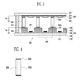
- FIG. 3 is a sectional view schematically illustrating the structure of the electron emission display device according to the embodiment shown in FIG. 2.
- the electron emission display device includes an electron emission substrate 100 in which at least one electron emission device 160 is disposed and an auxiliary electrode 180 is electrically connected to regions where the electron emission device 160 is not formed, an image forming substrate 200 having an image implementing part corresponding to the electron emission device 160, and spacers 320 positioned on the auxiliary electrode 180 of the electron emission substrate 100 to support the auxiliary electrode 180 to be spaced apart from the image forming substrate 200.
- the electron emission substrate 100 includes an electron emitting region in which a plurality of electron emission devices 160 are arranged in regions where cathode electrode wires cross gate electrode wires in a predetermined form. In one embodiment, the wires cross in a matrix form.
- Each of the electron emission devices 160 includes a cathode electrode 120, a gate electrode 140 crossing the cathode electrode 120, a first insulating layer 130 for insulating positioned between the two electrodes 120 and 140, a second insulating layer 170 formed on the gate electrode 140, and an auxiliary electrode 180 formed on the second insulating layer 170.
- the electron emission substrate 100 also includes an electron emitting part 150 electrically connected to the cathode electrode 120.
- the electron emission device corresponds to phosphors 230 formed on the image forming substrate 200.
- a bottom substrate 110 On a bottom substrate 110, at least one cathode electrode 120 is disposed in a predetermined shape, for example in a stripe shape.
- the bottom substrate 110 is generally glass or a silicon substrate.
- a transparent substrate, such as glass, is used in one embodiment for forming the electron emitting part 150 with carbon nanotube paste for bottom exposure.
- the cathode electrode 120 supplies a data signal and a scanning signal respectively transmitted from a data driving part (not shown) and a scanning driving part (not shown) to respective electron emission devices.
- each of the electron emission devices 160 includes the electron emitting part 150 formed in the region where the cathode electrode 120 crosses the gate electrode 140.
- the first insulating layer 130 is formed on the cathode electrode 120 and electrically insulates the cathode electrode 120 from the gate electrode 140.
- the first insulating layer 130 is made of insulating material, such as a glass mixture of PbO and SiO 2 .
- the gate electrode 140 is formed on the first insulating layer 130 in a predetermined shape, for example, in a stripe shape, and is arranged to cross the cathode electrode 120.
- the gate electrode 140 supplies the data signal or the scanning signal respectively transmitted from the data driving part or the scanning driving part to the respective electron emission devices.
- the gate electrode 140 is made of metal with excellent conductivity such as gold (Au), silver (Ag), platinum (Pt), aluminum (Al), chrome (Cr), or at least one of alloys of gold (Au), silver (Ag), platinum (Pt), aluminum (Al), chrome (Cr).
- the second insulating layer 170 is formed on the gate electrode 140, and electrically insulates the gate electrode 140 from the auxiliary electrode 180.
- the second insulating layer 170 is made of insulating material, such as a glass mixture of PbO and SiO 2 .
- the auxiliary electrode 180 is formed on the upper side of the second insulating layer 170 and is made of a metal with excellent conductivity such as gold (Au), silver (Ag), platinum (Pt), aluminum (Al), chrome (Cr), or at least one alloy of gold (Au), silver (Ag), platinum (Pt), aluminum (Al), chrome (Cr).
- a metal with excellent conductivity such as gold (Au), silver (Ag), platinum (Pt), aluminum (Al), chrome (Cr), or at least one alloy of gold (Au), silver (Ag), platinum (Pt), aluminum (Al), chrome (Cr).
- the auxiliary electrode 180 prevents the cathode electrode 120 and the gate electrode 140 from damage when arc discharging, and protects the cathode electrode 120, the gate electrode 140, and the electron emitting part 150 from the anode electric field generated due to high voltage applied to the anode electrode 220.
- Openings 155 penetrate the first insulating layers 130, the gate electrodes 140, the second insulating layers 170, and the auxiliary electrodes 180, which are sequentially laminated.
- the openings 155 expose the cathode electrodes 120.
- the openings 155 are regions where the electron emitting parts 150 are formed. In other words, at least one opening 155 is formed in the regions where the cathode electrodes 120 cross the gate electrodes 140.
- the electron emitting parts 150 are respectively electrically connected to the cathode electrodes exposed by the openings 155, and, in some embodiments, are made of carbon nanotube, graphite, graphite nanofiber, diamond-like carbon, C 60 , silicon nanowire, or a combination thereof.
- the image forming substrate 200 includes image forming regions having the anode electrode 220, the phosphors 230 formed on the anode electrode 220 to emit light due to electrons emitted by the electron emission devices 160, and light shielding films 240 formed between the phosphors 230.
- the anode electrode 220 is positioned on a top substrate 210, and successfully collects the electrons emitted from the electron emission devices 160. For the collection of the emitted electrons, a positive (+) high voltage is applied to the anode electrode 220 such that the emitted electrons are accelerated toward the phosphors 230.
- the top substrate 210 and the anode electrode 220 are made of transparent material.
- the top substrate is made of glass and the anode electrode 220 is made of ITO electrode so that light emitted from the phosphors 230 can be transmitted to the outside.
- the phosphors 230 for emitting light due to the collision of the electrons emitted from the electron emitting parts 150 are selectively arranged at predetermined intervals.
- a G-phosphor that is, a phosphor for emitting green light
- ZnS:Cu, Zn 2 SiO 4 :Mn, ZnS:Cu+Zn 2 SiO 4 :Mn Gd 2 O 2 S:Tb, Y 3 Al 5 O 12 :Ce, ZnS:Cu, Al, Y 2 O 2 S:Tb, ZnO:Zn, ZnS:Cu, Al+In 2 O 3 , LaPO 4 :Ce, Tb, BaO ⁇ 6Al 2 O 3 :Mn, (Zn, Cd)S:Ag, (Zn, Cd)S:Cu,Al,ZnS:Cu,Au,Al, Y 3 (Al, Ga) 2 O 12 :Tb, Y 2 SiO 5 :Tb,
- ZnS:Cu, Al is used.
- a B-phosphor i.e. a phosphor for emitting blue light
- ZnS:Ag, ZnS:Ag,Al, ZnS:Ag,Ga,Al, ZnS:Ag,Cu,Ga,Cl, ZnS:Ag+In 2 O 3 Ca 2 B 5 O 9 Cl:Eu 2+ , (Sr, Ca, Ba, Mg) 10 (PO 4 ) 6 Cl 2 :Eu 2+ , Sr 10 (PO 4 ) 6 C 2 :Eu 2+ , BaMgAl 16 O 26 :Eu 2+ , CoO,Al 2 O 3 are added ZnS:Ag, CoO,Al 2 O 3 are added ZnS:Ag,Ga are used, and in this embodiment, ZnS:Ag,Cl is used.
- R-phosphor that is, a phosphor for emitting red light
- Y 2 O 2 S:Eu, Zn 3 (PO 4 ) 2 :Mn, Y 2 O 3 :Eu, YVO 4 :Eu, (Y, Gd)BO 3 :Eu, ⁇ -Zn 3 (PO 4 ) 2 :Mn, (ZnCd)S:Ag, (ZnCd)S:Ag+In 2 O 3 , or Fe 2 O 3 added to Y 2 O 2 S:Eu may be used.
- Y 2 O 2 S:Eu is used.
- the phosphors 230 indicate independent monochrome phosphors. Although the phosphors 230 are disclosed as the phosphors for respectively emitting red-, green-, and blue-lights in this embodiment, the invention is not limited to these.
- the top substrate 210 in one embodiment, is made of transparent material to transmit light emitted from the phosphors 230 to the outside.
- the light shielding films 240 absorb and intercept external light and are arranged between the phosphors 230 at predetermined intervals such that cross talk is prevented to improve contrast.
- Metal reflecting films may be further formed on the phosphors 230 for successfully collecting electrons emitted from the electron emitting parts 150 and reflecting light generated due to the collision of the electrons toward the top substrate 210 to improve the reflection efficiency.
- Low resistance spacers 320 are positioned between the auxiliary electrodes 180 and the light shielding films 240, and are made of conductive material having insulation sufficient to endure a high voltage applied between the electron emission substrate 100 and the image forming substrate 200 and having conductivity sufficient to prevent charging the surfaces of the spacers 320.
- the low resistance spacers 320 are made of material having sufficient insulation, such as silicon glass, glass containing Na, solar-lime glass, alumina, or ceramic containing alumina. In one embodiment, the thermal expansion coefficient of the low resistance spacers 320 approximates the thermal expansion coefficient of the electron emission substrate 100 and the image forming substrate 200.
- the orbits of the electrons emitted from the electron emission substrate 100 are prevented from concentrating in the vicinity of the low resistance spacers 320 so that emission of different color light due to the orbit distortion of the electrons and the distortion and change of images due to the different color light emission can be reduced.
- the spacers 320 are attached to at least one of the electron emission substrate 100 and the image forming substrate 200 with conductive adhesives 330a and 330b, and, in this embodiment, are fixed by the adhesives 330a and 330b to the light shielding films 240 and the auxiliary electrodes 180.
- the electron emission display device 300 as described above further includes a sealer 310 for sealing the electron emission substrate 100 and the image forming substrate 200 and for maintaining a vacuum.
- FIG. 4 is a view schematically illustrating the structure of the spacer in FIG. 3.
- the low resistance spacers 320 are formed by adding conductive material having insulation sufficient to endure a high voltage applied between the electron emission substrate 100 and the image forming substrate 200 and conductivity sufficient to prevent charging the surfaces of the spacers 320.
- the low resistance spacers 320 are made of material having sufficient insulation, such as silicon glass, glass containing Na, solar-lime glass, alumina, or ceramic containing alumina.
- the thermal expansion coefficient of the low resistance spacers 320 approximates the thermal expansion coefficient of the electron emission substrate 100 and the image forming substrate 200.
- the low resistance spacers 320 include low resistance material 321 such that the surface charging of the spacers 320 is prevented and distortion of electron emission paths due to the spacers 320 or the surface charging thereof are prevented.
- the low resistance material 321 for implementing the low resistance of the low resistance spacers 320 is selected from material with a sufficiently low resistance, for example, metals such as Ni, Cr, Au, Mo, W, Pt, Ti, Al, Cu, and
- Pd alloys of Ni, Cr, Au, Mo, W, Pt, Ti, Al, Cu, and Pd, metals such as Pd, Ag, Au, and RuO 2 , metal oxide of Pd, Ag, Au, and RuO 2 , transparent conductors such as In 2 O 3 -SnO 2 , and semiconductors, such as poly silicon.
- the low resistance spacers 320 can have resistance ranging from 10 4 ⁇ cm to 10 14 ⁇ cm.
- low resistance materials 322 may be formed, and their resistance is equal to or less than the resistance of the adhesives 330a and 330b.
- a conductor layer having a higher conductivity than that of the low resistance spacers 320 may be formed.
- FIG. 5A is a view illustrating application of an anode voltage and an auxiliary electrode voltage to the electron emission display device having a low resistance spacer according to one embodiment of the present invention.
- an external power source applies a positive (+) voltage to the cathode electrode 120, a negative (-) voltage to the gate electrode 140, and a positive (+) voltage to the anode electrode 220.
- the cathode electrode 120 and the gate electrode 140 due to the voltage difference between the cathode electrode 120 and the gate electrode 140, the electric field is generated around the electron emitting parts 150 and the electrons are emitted therefrom, the emitted electrons are guided by high voltage applied to the anode electrode 220 to collide against the corresponding phosphors 230 such that the phosphors 230 emit light to form predetermined images.
- the auxiliary electrodes 180 apply the negative (-) voltage to the anode electrode 220 when applying the positive (+) voltage to the anode electrode 220, so that the electrons emitted from the electron emitting parts 150 are concentrated at the anode electrode 220.
- FIG. 5B is a view illustrating independently applying auxiliary electrode voltage to the electron emission display device having a low resistance spacer according to one embodiment of the present invention.
- a negative (-) voltage is independently applied to the auxiliary electrodes 180, so that electrons emitted from the electron emitting parts 150 are concentrated at the anode electrode 220.
- voltage ranging from -50V to +100V is independently applied to the auxiliary electrodes 220.
- FIG. 6 is a schematic view illustrating an electric field generated by applying the anode voltage and the auxiliary electrode voltage to the electron emission display device having a low resistance spacer according to the embodiment of the present invention as shown in FIGS. 5A and 5B.
- the orbits of the electrons emitted from the electron emitting parts are concentrated on the anode electrode 220 by the auxiliary electrodes 180 so that the electrons are prevented from being charged to the spacers 320.
- emission of different color light due to the orbit distortion of the electrons and the distortion and change of images due to the different color light emission can be reduced.
- charges are charged in the spacers by increasing the conductivity of the spacers so that the orbit distortion of the electron beams can be prevented.
- FIG. 7 is a schematic sectional view illustrating the structure of an electron emission display device according to another embodiment of the present invention
- FIG. 8 is a schematic view illustrating the low resistance spacer shown in FIG. 7.
- the electron emission display device 700 using low resistance spacers according to this embodiment of the present invention includes an electron emission substrate 100, in which at least one electron emission device is disposed, and auxiliary electrodes 718, electrically connected to portions of the electron emission substrate other than regions where the electron emission devices are formed.
- the electron emission display device also includes an image forming substrate 200, in which image implementing parts corresponding to the electron emission devices are formed, and low resistance spacers 730 for spacing the auxiliary electrodes 718 of the electron emission substrate 710 apart from the image forming substrate 200 to support the auxiliary electrodes 718.
- the spacers are formed by coating conductive material on the surfaces thereof.
- the low resistance spacers 730 are formed by coating the low resistance material 731 on spacer members for supporting the electron emission substrate 100 to be spaced apart from the corresponding image forming substrate 200.
- the low resistance spacers 730 are made of material as described above, such as silicon glass, glass containing Na, solar-lime glass, alumina, or ceramic containing alumina.
- the above-described conductive material 731 such as metal such as Ni, Cr, Au, Mo, W, Pt, Ti, Al, Cu, and Pd, alloys thereof Ni, Cr, Au, Mo, W, Pt, Ti, Al, Cu, and Pd, metal such as Pd, Ag, Au, RuO 2 , and
- Pd-Ag metal oxide of Pd, Ag, Au, RuO 2 , and Pd-Ag, transparent conductor such as In 2 O 3 -SnO 2 , and semiconductor such as poly silicon, is selected and coated.
- the low resistance spacers 730 can have resistance ranging from 10 4 ⁇ cm to 10 14 ⁇ cm. Moreover, on the sides of the low resistance spacers 730, low resistance materials 732 may be formed, and their resistance is equal to or less than the resistance of the adhesives 733a and 733b. On at least one of the sides of the low resistance spacers 730, a conductor layer having higher conductivity than that of the low resistance spacers 730, may be formed.
- FIG. 9 is a schematic sectional view illustrating the structure of an electron emission display device according to another embodiment of the present invention
- FIG. 10 is a schematic view illustrating the structure of a low resistance spacer shown in FIG. 9.
- the electron emission display device using low resistance spacers includes an electron emission substrate 100, in which at least one electron emission device is disposed, and auxiliary electrodes 918, electrically connected to portions of the electron emission substrate other than the regions where the electron emission devices are formed.
- This embodiment also includes an image forming substrate 200, in which image implementing parts corresponding to the electron emission devices are formed, and low resistance spacers 930 for spacing the auxiliary electrodes 918 of the electron emission substrate 100 apart from the image forming substrate 200 to support the auxiliary electrodes 918.
- the spacers are formed by doubly coating conductive material having different resistance to the image forming substrate 200.
- the low resistance spacers 930 for supporting the electron emission substrate to be spaced apart from the corresponding image forming substrate are coated with first and second low resistance materials 931 and 932.
- the description of the spacers is as described above in relation to FIG. 8, and is therefore omitted.
- the first low resistance material 931 and the second low resistance material 932 include materials with different resistances.
- the conductive material coated firstly may be a metal such as Ni, Cr, Au, Mo, W, Pt, Ti, Al, Cu, and Pd, an alloy of Ni, Cr, Au, Mo, W, Pt, Ti, Al, Cu, and Pd, a metal such as Pd, Ag, Au, RuO 2 , and Pd-Ag, a metal oxide of Pd, Ag, Au, RuO 2 , and Pd-Ag, a transparent conductor such as In 2 O 3 -SnO 2 , or a semiconductor such as poly silicon.
- the conductive material coated secondly has a resistance different from the conductive material coated firstly.
- the low resistance spacers 930 can have a resistance ranging from 10 4 ⁇ cm to 10 14 ⁇ cm. Moreover, on the sides of the low resistance spacers 930, low resistance materials 932 may be formed, and their resistance may be equal to or less than the resistance of the adhesives 933a and 933b. On at least one of the sides of the low resistance spacers 930, a conductor layer having higher conductivity than that of the low resistance spacers 930 may be formed.
Landscapes
- Cathode-Ray Tubes And Fluorescent Screens For Display (AREA)
- Vessels, Lead-In Wires, Accessory Apparatuses For Cathode-Ray Tubes (AREA)
Abstract
Description
- An electron emission display device includes a cathode substrate, an anode substrate, a line-shaped cathode electrode disposed on a surface of the cathode substrate, and a line-shaped anode electrode disposed on a surface of the anode substrate to cross the cathode electrode in perpendicular relationship. On the surface of the cathode electrode is an electron emitting part for emitting electrons when an electric field is generated. On the surface of the anode electrode is the luminescent layer for emitting light when the electrons are emitted from the electron emitting part. On the anode substrate between the anode electrodes, spacers are disposed. The spacers prevent the substrates from deformation or damage when sealing the cathode substrate and the anode substrate under high vacuum.
- FIG. 1 is a sectional view illustrating a part of the conventional electron emission display device having a spacer.
- As shown in FIG. 1, in the conventional electron emission display device, a line-
shaped cathode electrode 22 is disposed on a surface of acathode substrate 21 and a surface typeelectron emitting part 23 is disposed on thecathode electrode 22. On ananode electrode substrate 11 facing thecathode substrate 21, line-shaped anode electrodes 12 cross thecathode electrode 22 in perpendicular relationship and are so disposed. On the anode electrodes,luminescent layers 14, in which electrons emitted from theelectron emitting part 23 collide against and emit light, are disposed. Between theanode electrodes 12,auxiliary spacers 34a serving as a light-shielding film are disposed. In regions where theanode substrate 11 adheres to thecathode substrate 21, a plurality ofspacers 34 are arranged at predetermined intervals. Thespacers 34 are adhered with one of theanode substrate 11 and thecathode substrate 21 by ftits. - Thus, when the
spacers 34 adhere to theanode substrate 11 or thecathode substrate 21 due to the frit, a distance between theanode substrate 11 and the cathode substrate 21 (which may be predetermined) is maintained by thespacers 34. - However, some of the emitted electrons collide against the spacers in the vicinity of the spacers, or ions generated by the emitted electrons are attached to the spacers and charge the spacers. Since the charged electrons do not smoothly discharge electricity because of high resistance of the spacers, orbits of the electrons emitted by the electron emission devices are changed due to charge of the spacers and the emitted electrons arrive at other places than the corresponding phosphors so that distorted images are generated in the vicinity of the spacers.
- An electron emission display device includes an electron emission substrate; an electron emission device disposed on a region of the electron emission substrate; an auxiliary electrode electrically connected to the electron emission substrate at a portion other than the region where the electron emission device is disposed; an image forming substrate; an image implementing part corresponding to the electron emission device disposed on the image forming substrate; and a spacer for supporting the auxiliary electrode and the image forming substrate to be spaced apart from each other, the spacer including a conductive material.
- In one embodiment, the spacer is fixed to at least one of the electron emission substrate or the image forming substrate by an adhesive, and the adhesive includes conductive material. On at least one side of the spacer may be located a low resistance material having a resistance equal to or less than a resistance of the adhesive. In one embodiment, the spacer has a resistance ranging from 104 Ωcm to 1014 Ωcm.
- The conductive material of the spacer may include one metal selected from the group consisting of Ni, Cr, Au, Ag, Mo, W, Pt, Ti, Al, Cu, and Pd, one alloy selected from the group consisting of Ni, Cr, Au, Mo, W, Pt, Ti, Al, Cu, and Pd, one metal oxide selected from the group consisting of In2O3-SnO2 and RuO2, or poly silicon.
- In one embodiment, on least one side of the spacer is located a conductor layer having a higher conductivity than that of the spacer, and the electron emission device includes: a cathode electrode; an electron emitting part electrically connected to the cathode electrode; a first insulating layer formed on the cathode electrode; a gate electrode crossing the cathode electrode to emit electrons from the electron emitting part; a second insulating layer formed on the gate electrode; and the auxiliary electrode formed on the second insulating layer to collect the electrons emitted by the gate electrode.
- In another embodiment, an external power source independently applies voltage ranging from -50V to +100V to the auxiliary electrode. The image implementing part may include: luminescent layers emitting light due to electrons emitted from the electron emission device; a light shielding film disposed between the luminescent layers; and an anode electrode electrically connected to the luminescent layers.
- A voltage may be applied to the anode electrode and a negative voltage corresponding to voltage applied to the anode electrode may be applied to the auxiliary electrode.
- Another embodiment of an electron emission display device includes: an electron emission substrate; an electron emission device disposed on a region of the electron emission substrate; an auxiliary electrode electrically connected to the electron emission substrate at a portion other than the region where the electron emission device is disposed; an image forming substrate; an image implementing part corresponding to the electron emission device disposed on the image forming substrate; and a spacer for supporting the auxiliary electrode and the image forming substrate to be spaced apart from each other, the spacer being coated with a conductive material.
- The conductive material coating the spacer may include one metal selected from the group consisting of Ni, Cr, Au, Ag, Mo, W, Pt, Ti, Al, Cu, and Pd, one alloy selected from the group consisting of Ni, Cr, Au, Mo, W, Pt, Ti, Al, Cu, and Pd, one metal oxide selected from the group consisting of RuO2 and In2O3-SnO2, or poly silicon, and the spacer may have a resistance ranging from 104 Ωcm to 1014 Ωcm.
- Another embodiment of an electron emission display device includes: an electron emission substrate; an electron emission device disposed on a region of the electron emission substrate; an auxiliary electrode electrically connected to the electron emission substrate at a portion other than the region where the electron emission device is disposed; an image forming substrate; an image implementing part corresponding to the electron emission device disposed on the image forming substrate; and a spacer for supporting the auxiliary electrode and the image forming substrate to be spaced apart from each other, the spacer having a first coating of a first conductive material and a second coating of a second conductive material, the first conductive material having a different resistance than the second conductive material.
- The first or second conductive material may include one metal selected from the group consisting of Ni, Cr, Au, Ag, Mo, W, Pt, Ti, Al, Cu, and Pd, one alloy selected from the group consisting of Ni, Cr, Au, Mo, W, Pt, Ti, Al, Cu, and Pd, one metal oxide selected from the group consisting of RuO2 and In2O3-SnO2, or poly silicon.
- In one embodiment, the spacer has a resistance ranging from 104 Ωcm to 1014 Ωcm, and is formed of an insulating material selected from the group consisting of silicon glass, glass containing Na, solar-lime glass, alumina, and ceramic containing alumina. In another embodiment, a thermal expansion coefficient of the spacer is approximately equal to a thermal expansion coefficient of the electron emission substrate and a thermal expansion coefficient of the image forming substrate.
- These and/or other aspects and features of various embodiments of the invention will become apparent and more readily appreciated from the following description of examples of embodiments, taken in conjunction with the accompanying drawings of which:
- FIG. 1 is a sectional view illustrating a part of a conventional electron emission display device having a spacer;
- FIG. 2 is an exploded perspective view schematically illustrating the structure of an electron emission display device according to an embodiment of the present invention;
- FIG. 3 is a sectional view schematically illustrating the structure of the electron emission display device according to the embodiment shown in FIG. 2;
- FIG. 4 is a view schematically illustrating the structure of the spacer in FIG. 3;
- FIG. 5A is a schematic view illustrating applying anode voltage and auxiliary electrode voltage to the electron emission display device having a low resistance spacer according to an embodiment of the present invention;
- FIG. 5B is a schematic view illustrating independently applying auxiliary electrode voltage to the electron emission display device having a low resistance spacer according to an embodiment of the present invention;
- FIG. 6 is a schematic view illustrating electric field generated by applying the anode voltage and auxiliary electrode voltage to the electron emission display device having a low resistance spacer according to the embodiment of the present invention as shown in FIGS. 5A and 5B;
- FIG. 7 is a schematic sectional view illustrating the structure of an electron emission display device according to another embodiment of the present invention;
- FIG. 8 is a schematic view illustrating a low resistance spacer in FIG. 7;
- FIG. 9 is a schematic sectional view illustrating the structure of an electron emission display device according to another embodiment of the present invention; and
- FIG. 10 is a schematic view illustrating the structure of a low resistance spacer in FIG. 9.
- Hereinafter, examples of embodiments according to the present invention will be described with reference to the accompanying drawings, wherein the described embodiments of the present invention are provided to be readily understood by those skilled in the art.
- FIG. 2 is an exploded perspective view schematically illustrating the structure of an electron emission display device according to one embodiment of the present invention, and FIG. 3 is a sectional view schematically illustrating the structure of the electron emission display device according to the embodiment shown in FIG. 2.
- As shown in FIGS. 2 and 3, the electron emission display device according to this embodiment of the present invention includes an
electron emission substrate 100 in which at least oneelectron emission device 160 is disposed and anauxiliary electrode 180 is electrically connected to regions where theelectron emission device 160 is not formed, animage forming substrate 200 having an image implementing part corresponding to theelectron emission device 160, andspacers 320 positioned on theauxiliary electrode 180 of theelectron emission substrate 100 to support theauxiliary electrode 180 to be spaced apart from theimage forming substrate 200. - The
electron emission substrate 100 includes an electron emitting region in which a plurality ofelectron emission devices 160 are arranged in regions where cathode electrode wires cross gate electrode wires in a predetermined form. In one embodiment, the wires cross in a matrix form. Each of theelectron emission devices 160 includes acathode electrode 120, agate electrode 140 crossing thecathode electrode 120, a firstinsulating layer 130 for insulating positioned between the twoelectrodes insulating layer 170 formed on thegate electrode 140, and anauxiliary electrode 180 formed on the secondinsulating layer 170. Theelectron emission substrate 100 also includes anelectron emitting part 150 electrically connected to thecathode electrode 120. The electron emission device corresponds tophosphors 230 formed on theimage forming substrate 200. - On a
bottom substrate 110, at least onecathode electrode 120 is disposed in a predetermined shape, for example in a stripe shape. Thebottom substrate 110 is generally glass or a silicon substrate. A transparent substrate, such as glass, is used in one embodiment for forming theelectron emitting part 150 with carbon nanotube paste for bottom exposure. - The
cathode electrode 120 supplies a data signal and a scanning signal respectively transmitted from a data driving part (not shown) and a scanning driving part (not shown) to respective electron emission devices. Here, each of theelectron emission devices 160 includes theelectron emitting part 150 formed in the region where thecathode electrode 120 crosses thegate electrode 140. - The first
insulating layer 130 is formed on thecathode electrode 120 and electrically insulates thecathode electrode 120 from thegate electrode 140. The first insulatinglayer 130 is made of insulating material, such as a glass mixture of PbO and SiO2. - The
gate electrode 140 is formed on the first insulatinglayer 130 in a predetermined shape, for example, in a stripe shape, and is arranged to cross thecathode electrode 120. Thegate electrode 140 supplies the data signal or the scanning signal respectively transmitted from the data driving part or the scanning driving part to the respective electron emission devices. Thegate electrode 140 is made of metal with excellent conductivity such as gold (Au), silver (Ag), platinum (Pt), aluminum (Al), chrome (Cr), or at least one of alloys of gold (Au), silver (Ag), platinum (Pt), aluminum (Al), chrome (Cr). - The second
insulating layer 170 is formed on thegate electrode 140, and electrically insulates thegate electrode 140 from theauxiliary electrode 180. The secondinsulating layer 170 is made of insulating material, such as a glass mixture of PbO and SiO2. - The
auxiliary electrode 180 is formed on the upper side of the second insulatinglayer 170 and is made of a metal with excellent conductivity such as gold (Au), silver (Ag), platinum (Pt), aluminum (Al), chrome (Cr), or at least one alloy of gold (Au), silver (Ag), platinum (Pt), aluminum (Al), chrome (Cr). - The
auxiliary electrode 180 prevents thecathode electrode 120 and thegate electrode 140 from damage when arc discharging, and protects thecathode electrode 120, thegate electrode 140, and theelectron emitting part 150 from the anode electric field generated due to high voltage applied to theanode electrode 220. -
Openings 155 penetrate the first insulatinglayers 130, thegate electrodes 140, the second insulatinglayers 170, and theauxiliary electrodes 180, which are sequentially laminated. Theopenings 155 expose thecathode electrodes 120. Theopenings 155 are regions where theelectron emitting parts 150 are formed. In other words, at least oneopening 155 is formed in the regions where thecathode electrodes 120 cross thegate electrodes 140. - The
electron emitting parts 150 are respectively electrically connected to the cathode electrodes exposed by theopenings 155, and, in some embodiments, are made of carbon nanotube, graphite, graphite nanofiber, diamond-like carbon, C60, silicon nanowire, or a combination thereof. - The
image forming substrate 200 includes image forming regions having theanode electrode 220, thephosphors 230 formed on theanode electrode 220 to emit light due to electrons emitted by theelectron emission devices 160, andlight shielding films 240 formed between thephosphors 230. - The
anode electrode 220 is positioned on atop substrate 210, and successfully collects the electrons emitted from theelectron emission devices 160. For the collection of the emitted electrons, a positive (+) high voltage is applied to theanode electrode 220 such that the emitted electrons are accelerated toward thephosphors 230. - The
top substrate 210 and theanode electrode 220, in one embodiment, are made of transparent material. For example, the top substrate is made of glass and theanode electrode 220 is made of ITO electrode so that light emitted from thephosphors 230 can be transmitted to the outside. - On the
top substrate 210, thephosphors 230 for emitting light due to the collision of the electrons emitted from theelectron emitting parts 150 are selectively arranged at predetermined intervals. As a G-phosphor, that is, a phosphor for emitting green light, ZnS:Cu, Zn2SiO4:Mn, ZnS:Cu+Zn2SiO4:Mn, Gd2O2S:Tb, Y3Al5O12:Ce, ZnS:Cu, Al, Y2O2S:Tb, ZnO:Zn, ZnS:Cu, Al+In2O3, LaPO4:Ce, Tb, BaO·6Al2O3:Mn, (Zn, Cd)S:Ag, (Zn, Cd)S:Cu,Al,ZnS:Cu,Au,Al, Y3(Al, Ga)2O12:Tb, Y2SiO5:Tb, or LaOCl:Tb may be used. In this embodiment, ZnS:Cu, Al, is used. Moreover, as a B-phosphor, i.e. a phosphor for emitting blue light, ZnS:Ag, ZnS:Ag,Al, ZnS:Ag,Ga,Al, ZnS:Ag,Cu,Ga,Cl, ZnS:Ag+In2O3, Ca2B5O9Cl:Eu2+, (Sr, Ca, Ba, Mg)10(PO4)6Cl2:Eu2+, Sr10(PO4)6C2:Eu2+, BaMgAl16O26:Eu2+ , CoO,Al 2 O 3 are added ZnS:Ag, CoO,Al 2 O 3 are added ZnS:Ag,Ga are used, and in this embodiment, ZnS:Ag,Cl is used. As an R-phosphor, that is, a phosphor for emitting red light, Y2O2S:Eu, Zn3(PO4)2:Mn, Y2O3:Eu, YVO4:Eu, (Y, Gd)BO3:Eu, γ-Zn3(PO4)2:Mn, (ZnCd)S:Ag, (ZnCd)S:Ag+In2O3, or Fe2O3 added to Y2O2S:Eu may be used. In this embodiment, Y2O2S:Eu is used. - The
phosphors 230 indicate independent monochrome phosphors. Although thephosphors 230 are disclosed as the phosphors for respectively emitting red-, green-, and blue-lights in this embodiment, the invention is not limited to these. Thetop substrate 210, in one embodiment, is made of transparent material to transmit light emitted from thephosphors 230 to the outside. - The
light shielding films 240 absorb and intercept external light and are arranged between thephosphors 230 at predetermined intervals such that cross talk is prevented to improve contrast. - Metal reflecting films (not shown) may be further formed on the
phosphors 230 for successfully collecting electrons emitted from theelectron emitting parts 150 and reflecting light generated due to the collision of the electrons toward thetop substrate 210 to improve the reflection efficiency. -
Low resistance spacers 320 are positioned between theauxiliary electrodes 180 and thelight shielding films 240, and are made of conductive material having insulation sufficient to endure a high voltage applied between theelectron emission substrate 100 and theimage forming substrate 200 and having conductivity sufficient to prevent charging the surfaces of thespacers 320. - The
low resistance spacers 320 are made of material having sufficient insulation, such as silicon glass, glass containing Na, solar-lime glass, alumina, or ceramic containing alumina. In one embodiment, the thermal expansion coefficient of thelow resistance spacers 320 approximates the thermal expansion coefficient of theelectron emission substrate 100 and theimage forming substrate 200. - Thus, the orbits of the electrons emitted from the
electron emission substrate 100 are prevented from concentrating in the vicinity of thelow resistance spacers 320 so that emission of different color light due to the orbit distortion of the electrons and the distortion and change of images due to the different color light emission can be reduced. - In one embodiment, the
spacers 320 are attached to at least one of theelectron emission substrate 100 and theimage forming substrate 200 withconductive adhesives adhesives light shielding films 240 and theauxiliary electrodes 180. - The electron
emission display device 300 as described above further includes asealer 310 for sealing theelectron emission substrate 100 and theimage forming substrate 200 and for maintaining a vacuum. - FIG. 4 is a view schematically illustrating the structure of the spacer in FIG. 3. As shown in the drawing, the
low resistance spacers 320 are formed by adding conductive material having insulation sufficient to endure a high voltage applied between theelectron emission substrate 100 and theimage forming substrate 200 and conductivity sufficient to prevent charging the surfaces of thespacers 320. - In more detail, the
low resistance spacers 320 are made of material having sufficient insulation, such as silicon glass, glass containing Na, solar-lime glass, alumina, or ceramic containing alumina. In this embodiment, the thermal expansion coefficient of thelow resistance spacers 320 approximates the thermal expansion coefficient of theelectron emission substrate 100 and theimage forming substrate 200. - The
low resistance spacers 320 includelow resistance material 321 such that the surface charging of thespacers 320 is prevented and distortion of electron emission paths due to thespacers 320 or the surface charging thereof are prevented. Thelow resistance material 321 for implementing the low resistance of thelow resistance spacers 320 is selected from material with a sufficiently low resistance, for example, metals such as Ni, Cr, Au, Mo, W, Pt, Ti, Al, Cu, and - Pd, alloys of Ni, Cr, Au, Mo, W, Pt, Ti, Al, Cu, and Pd, metals such as Pd, Ag, Au, and RuO2, metal oxide of Pd, Ag, Au, and RuO2, transparent conductors such as In2O3-SnO2, and semiconductors, such as poly silicon.
- By doing so, the
low resistance spacers 320 can have resistance ranging from 104 Ωcm to 1014 Ωcm. - On the sides of the
low resistance spacers 320,low resistance materials 322 may be formed, and their resistance is equal to or less than the resistance of theadhesives low resistance spacers 320, a conductor layer having a higher conductivity than that of thelow resistance spacers 320 may be formed. - FIG. 5A is a view illustrating application of an anode voltage and an auxiliary electrode voltage to the electron emission display device having a low resistance spacer according to one embodiment of the present invention. As shown in the drawing, in the electron
emission display device 300 having thelow resistance spacers 320, an external power source applies a positive (+) voltage to thecathode electrode 120, a negative (-) voltage to thegate electrode 140, and a positive (+) voltage to theanode electrode 220. By doing so, due to the voltage difference between thecathode electrode 120 and thegate electrode 140, the electric field is generated around theelectron emitting parts 150 and the electrons are emitted therefrom, the emitted electrons are guided by high voltage applied to theanode electrode 220 to collide against the correspondingphosphors 230 such that thephosphors 230 emit light to form predetermined images. - At that time, the
auxiliary electrodes 180 apply the negative (-) voltage to theanode electrode 220 when applying the positive (+) voltage to theanode electrode 220, so that the electrons emitted from theelectron emitting parts 150 are concentrated at theanode electrode 220. - FIG. 5B is a view illustrating independently applying auxiliary electrode voltage to the electron emission display device having a low resistance spacer according to one embodiment of the present invention. As shown in the drawing, a negative (-) voltage is independently applied to the
auxiliary electrodes 180, so that electrons emitted from theelectron emitting parts 150 are concentrated at theanode electrode 220. At that time, voltage ranging from -50V to +100V is independently applied to theauxiliary electrodes 220. - FIG. 6 is a schematic view illustrating an electric field generated by applying the anode voltage and the auxiliary electrode voltage to the electron emission display device having a low resistance spacer according to the embodiment of the present invention as shown in FIGS. 5A and 5B. As shown in the drawing, in the electron emission display device including the auxiliary electrodes, the orbits of the electrons emitted from the electron emitting parts are concentrated on the
anode electrode 220 by theauxiliary electrodes 180 so that the electrons are prevented from being charged to thespacers 320. Thus, emission of different color light due to the orbit distortion of the electrons and the distortion and change of images due to the different color light emission can be reduced. - Moreover, charges are charged in the spacers by increasing the conductivity of the spacers so that the orbit distortion of the electron beams can be prevented.
- FIG. 7 is a schematic sectional view illustrating the structure of an electron emission display device according to another embodiment of the present invention, and FIG. 8 is a schematic view illustrating the low resistance spacer shown in FIG. 7. As shown in the drawing, the electron
emission display device 700 using low resistance spacers according to this embodiment of the present invention includes anelectron emission substrate 100, in which at least one electron emission device is disposed, andauxiliary electrodes 718, electrically connected to portions of the electron emission substrate other than regions where the electron emission devices are formed. The electron emission display device also includes animage forming substrate 200, in which image implementing parts corresponding to the electron emission devices are formed, andlow resistance spacers 730 for spacing theauxiliary electrodes 718 of the electron emission substrate 710 apart from theimage forming substrate 200 to support theauxiliary electrodes 718. The spacers are formed by coating conductive material on the surfaces thereof. - The
low resistance spacers 730 are formed by coating thelow resistance material 731 on spacer members for supporting theelectron emission substrate 100 to be spaced apart from the correspondingimage forming substrate 200. - The
low resistance spacers 730 are made of material as described above, such as silicon glass, glass containing Na, solar-lime glass, alumina, or ceramic containing alumina. - On the surfaces of the
spacers 730, the above-describedconductive material 731, such as metal such as Ni, Cr, Au, Mo, W, Pt, Ti, Al, Cu, and Pd, alloys thereof Ni, Cr, Au, Mo, W, Pt, Ti, Al, Cu, and Pd, metal such as Pd, Ag, Au, RuO2, and - Pd-Ag, metal oxide of Pd, Ag, Au, RuO2, and Pd-Ag, transparent conductor such as In2O3-SnO2, and semiconductor such as poly silicon, is selected and coated.
- By doing so, the
low resistance spacers 730 can have resistance ranging from 104 Ωcm to 1014 Ωcm. Moreover, on the sides of thelow resistance spacers 730,low resistance materials 732 may be formed, and their resistance is equal to or less than the resistance of theadhesives low resistance spacers 730, a conductor layer having higher conductivity than that of thelow resistance spacers 730, may be formed. - FIG. 9 is a schematic sectional view illustrating the structure of an electron emission display device according to another embodiment of the present invention, and FIG. 10 is a schematic view illustrating the structure of a low resistance spacer shown in FIG. 9. The electron emission display device using low resistance spacers according to this embodiment of the present invention includes an
electron emission substrate 100, in which at least one electron emission device is disposed, andauxiliary electrodes 918, electrically connected to portions of the electron emission substrate other than the regions where the electron emission devices are formed. This embodiment also includes animage forming substrate 200, in which image implementing parts corresponding to the electron emission devices are formed, andlow resistance spacers 930 for spacing theauxiliary electrodes 918 of theelectron emission substrate 100 apart from theimage forming substrate 200 to support theauxiliary electrodes 918. The spacers are formed by doubly coating conductive material having different resistance to theimage forming substrate 200. - The
low resistance spacers 930 for supporting the electron emission substrate to be spaced apart from the corresponding image forming substrate are coated with first and secondlow resistance materials - The first
low resistance material 931 and the secondlow resistance material 932 include materials with different resistances. For example, the conductive material coated firstly may be a metal such as Ni, Cr, Au, Mo, W, Pt, Ti, Al, Cu, and Pd, an alloy of Ni, Cr, Au, Mo, W, Pt, Ti, Al, Cu, and Pd, a metal such as Pd, Ag, Au, RuO2, and Pd-Ag, a metal oxide of Pd, Ag, Au, RuO2, and Pd-Ag, a transparent conductor such as In2O3-SnO2, or a semiconductor such as poly silicon. The conductive material coated secondly has a resistance different from the conductive material coated firstly. - By doing so, the
low resistance spacers 930 can have a resistance ranging from 104 Ωcm to 1014 Ωcm. Moreover, on the sides of thelow resistance spacers 930,low resistance materials 932 may be formed, and their resistance may be equal to or less than the resistance of theadhesives 933a and 933b. On at least one of the sides of thelow resistance spacers 930, a conductor layer having higher conductivity than that of thelow resistance spacers 930 may be formed.
Claims (17)
- An electron emission display device (300, 700, 900) comprising:an electron emission substrate (100);an electron emission device (160) disposed on a region of the electron emission substrate (100);an auxiliary electrode (180, 718, 918) electrically connected to the electron emission substrate (100) at a portion other than the region where the electron emission device (160) is disposed;an image forming substrate (200);an image implementing part corresponding to the electron emission device (160) disposed on the image forming substrate (200); anda spacer (320, 730, 930) for supporting the auxiliary electrode (180, 718, 918) and the image forming substrate (200) to be spaced apart from each other, the spacer (320, 730, 930) comprising at least a first conductive material (321, 731, 931).
- The electron emission display device (300) according to claim 1, wherein the bulk of the spacer (320) consists of the first conductive material (321).
- The electron emission display device (700) according to claim 1, wherein the spacer (730) is coated with the first conductive material (731).
- The electron emission display device (900) of claim 1, wherein the spacer (930) has a first coating of the first conductive material (931) and a second coating of a second conductive material (932), the first conductive material (931) having a different resistance than the second conductive material (932).
- The electron emission display device (900) according to claim 4, wherein the second conductive material (932) comprises one metal selected from the group consisting of Ni, Cr, Au, Ag, Mo, W, Pt, Ti, Al, Cu, and Pd, one alloy selected from the group consisting of Ni, Cr, Au, Mo, W, Pt, Ti, Al, Cu, and Pd, one metal oxide selected from the group consisting of RuO2 and In2O3-SnO2, or poly silicon.
- The electron emission display device (300, 700, 900) according to one of the preceding claims, wherein the first conductive material (321, 731, 931) comprises one metal selected from the group consisting of Ni, Cr, Au, Ag, Mo, W, Pt, Ti, Al, Cu, and Pd, one alloy selected from the group consisting of Ni, Cr, Au, Mo, W, Pt, Ti, Al, Cu, and Pd, one metal oxide selected from the group consisting of RuO2 and In2O3-SnO2, or poly silicon.
- The electron emission display device (300, 700, 900) according to one of the preceding claims, wherein the spacer (320, 730, 930) is fixed to at least one of the electron emission substrate (100) or the image forming substrate (200) by an adhesive (330a, 330b, 733a, 733b, 933a, 933b).
- The electron emission display device (300, 700, 900) according to claim 7, wherein the adhesive (330a, 330b, 733a, 733b, 933a, 933b) comprises a third conductive material.
- The electron emission display device (300, 700, 900) according to claim 7 or 8, wherein on at least one side of the spacer (320, 730, 930) is located a low resistance material (322, 732, 934) having a resistance equal to or less than a resistance of the adhesive (330a, 330b, 733a, 733b, 933a, 933b).
- The electron emission display device (300, 700, 900) according to one of the preceding claims, wherein the spacer (320, 730, 930) has a resistance ranging from 104 Ωcm to 1014 Ωcm.
- The electron emission display device (300, 700, 900) according to one of the preceding claims, wherein on least one side of the spacer (320, 730, 930) is located a conductor layer having a higher conductivity than that of the spacer (320, 730, 930).
- The electron emission display device (300, 700, 900) according to one of the preceding claims, wherein the electron emission device (160) comprises:a cathode electrode (120);an electron emitting part (150) electrically connected to the cathode electrode (120);a first insulating layer (130) formed on the cathode electrode (120);a gate electrode (140) crossing the cathode electrode (120) to emit electrons from the electron emitting part (150);a second insulating layer (170) formed on the gate electrode (140); andthe auxiliary electrode (180, 718, 918) formed on the second insulating layer (170) to collect the electrons emitted by the gate electrode (140).
- The electron emission display device (300, 700, 900) according to claim 12, wherein an external power source independently applies voltage ranging from -50V to +100V to the auxiliary electrode.
- The electron emission display device (300, 700, 900) according to one of the preceding claims, wherein the image implementing part comprises:luminescent layers (230) emitting light due to electrons emitted from the electron emission device (160);a light shielding film (240) disposed between the luminescent layers (230); andan anode electrode (220) electrically connected to the luminescent layers (230).
- The electron emission display device (300, 700, 900) according to claim 14, wherein a voltage is applied to the anode electrode (220) and a negative voltage corresponding to voltage applied to the anode electrode (220) is applied to the auxiliary electrode (180, 718, 918).
- The electron emission display device (300, 700, 900) according to one of the preceding claims, wherein the spacer (320, 730, 930) is formed of an insulating material selected from the group consisting of silicon glass, glass containing Na, solar-lime glass, alumina, and ceramic containing alumina.
- The electron emission display device (300, 700, 900) according to one of the preceding claims, wherein a thermal expansion coefficient of the spacer (320, 730, 930) is approximately equal to a thermal expansion coefficient of the electron emission substrate (100) and a thermal expansion coefficient of the image forming substrate (200).
Applications Claiming Priority (1)
| Application Number | Priority Date | Filing Date | Title |
|---|---|---|---|
| KR1020050069811A KR20070014840A (en) | 2005-07-29 | 2005-07-29 | Electronic emission display device using low resistance spacer |
Publications (2)
| Publication Number | Publication Date |
|---|---|
| EP1748463A2 true EP1748463A2 (en) | 2007-01-31 |
| EP1748463A3 EP1748463A3 (en) | 2007-03-07 |
Family
ID=37075827
Family Applications (1)
| Application Number | Title | Priority Date | Filing Date |
|---|---|---|---|
| EP06118058A Withdrawn EP1748463A3 (en) | 2005-07-29 | 2006-07-28 | Electron emission display device having low resistance spacer |
Country Status (5)
| Country | Link |
|---|---|
| US (1) | US20070029921A1 (en) |
| EP (1) | EP1748463A3 (en) |
| JP (1) | JP2007042570A (en) |
| KR (1) | KR20070014840A (en) |
| CN (1) | CN1933089A (en) |
Families Citing this family (5)
| Publication number | Priority date | Publication date | Assignee | Title |
|---|---|---|---|---|
| KR20050096478A (en) * | 2004-03-30 | 2005-10-06 | 삼성에스디아이 주식회사 | Electron emission display and method for manufacturing the same |
| KR100891619B1 (en) * | 2007-07-02 | 2009-04-02 | 재단법인 구미전자정보기술원 | Method for manufacturing spacer for field emission device and field emission device accordingly |
| US9525554B2 (en) * | 2008-05-30 | 2016-12-20 | Google Inc. | Device and method for identifying a certificate for multiple identities of a user |
| JP4997202B2 (en) * | 2008-09-08 | 2012-08-08 | ソニー株式会社 | Flat display device and spacer |
| US20160152827A1 (en) * | 2014-12-02 | 2016-06-02 | Sabic Global Technologies B.V. | High flow polyetherimide-siloxane compositions, method of manufacture, and articles made therefrom |
Family Cites Families (16)
| Publication number | Priority date | Publication date | Assignee | Title |
|---|---|---|---|---|
| US4950939A (en) * | 1988-09-15 | 1990-08-21 | Galileo Electro-Optics Corp. | Channel electron multipliers |
| JP3083076B2 (en) * | 1995-04-21 | 2000-09-04 | キヤノン株式会社 | Image forming device |
| JP2776353B2 (en) * | 1995-12-27 | 1998-07-16 | 日本電気株式会社 | Field emission cold cathode |
| US5720640A (en) * | 1996-02-15 | 1998-02-24 | Industrial Technology Research Institute | Invisible spacers for field emission displays |
| DE69839985D1 (en) * | 1997-08-01 | 2008-10-23 | Canon Kk | Electron beam apparatus, image forming apparatus using this electron beam apparatus, components for electron beam apparatus, and methods of manufacturing these apparatus and components |
| US6262528B1 (en) * | 1997-11-28 | 2001-07-17 | Samsung Display Devices Co., Ltd. | Field emission display (FED) and method for assembling spacer of the same |
| US5990613A (en) * | 1998-01-20 | 1999-11-23 | Motorola, Inc. | Field emission device having a non-coated spacer |
| US5990614A (en) * | 1998-02-27 | 1999-11-23 | Candescent Technologies Corporation | Flat-panel display having temperature-difference accommodating spacer system |
| WO2000014764A1 (en) * | 1998-09-08 | 2000-03-16 | Canon Kabushiki Kaisha | Electron beam device, method for producing charging-suppressing member used in the electron beam device, and image forming device |
| JP4115050B2 (en) * | 1998-10-07 | 2008-07-09 | キヤノン株式会社 | Electron beam apparatus and spacer manufacturing method |
| US6841256B2 (en) * | 1999-06-07 | 2005-01-11 | Honeywell International Inc. | Low dielectric constant polyorganosilicon materials generated from polycarbosilanes |
| JP2002270099A (en) * | 2001-03-07 | 2002-09-20 | Sony Corp | Knocking method for flat display device and knocking method for flat display device substrate |
| JP2003323853A (en) * | 2002-05-01 | 2003-11-14 | Sony Corp | Cold cathode field emission display |
| JP2004311247A (en) * | 2003-04-08 | 2004-11-04 | Toshiba Corp | Image display device and method of manufacturing spacer assembly used for image display device |
| JP3944211B2 (en) * | 2004-01-05 | 2007-07-11 | キヤノン株式会社 | Image display device |
| KR20060095317A (en) * | 2005-02-28 | 2006-08-31 | 삼성에스디아이 주식회사 | Electron-emitting device |
-
2005
- 2005-07-29 KR KR1020050069811A patent/KR20070014840A/en not_active Ceased
- 2005-10-13 JP JP2005299230A patent/JP2007042570A/en active Pending
-
2006
- 2006-07-28 US US11/495,189 patent/US20070029921A1/en not_active Abandoned
- 2006-07-28 EP EP06118058A patent/EP1748463A3/en not_active Withdrawn
- 2006-07-31 CN CNA2006101323000A patent/CN1933089A/en active Pending
Also Published As
| Publication number | Publication date |
|---|---|
| JP2007042570A (en) | 2007-02-15 |
| EP1748463A3 (en) | 2007-03-07 |
| US20070029921A1 (en) | 2007-02-08 |
| CN1933089A (en) | 2007-03-21 |
| KR20070014840A (en) | 2007-02-01 |
Similar Documents
| Publication | Publication Date | Title |
|---|---|---|
| EP1172836A1 (en) | Front plate for field-emission display | |
| US20050184647A1 (en) | Electron emission device | |
| GB2399217A (en) | Flat panel display device | |
| US20070029921A1 (en) | Electron emission display device having low resistance spacer | |
| US20080012467A1 (en) | Method for Treating a Cathode Panel, Cold Cathode Field Emission Display Device, and Method for Producing the Same | |
| US20070290602A1 (en) | Image display device and manufacturing method of the same | |
| CN102148120A (en) | Symmetric quadrupole structure non-isolating support filed emission displayer | |
| EP1850366B1 (en) | Electron emission display device | |
| US7075223B2 (en) | Electron beam apparatus with potential specifying plate structure | |
| WO1999031699A1 (en) | Field emission device having a composite spacer | |
| US20060267477A1 (en) | Image display device | |
| EP1101238B1 (en) | Flat panel display walls and methods for forming such | |
| EP1619713A1 (en) | Image disply unit and production method for spacer assembly used in image display unit | |
| JP4077972B2 (en) | Image forming apparatus | |
| EP1780751B1 (en) | Spacer and electron emission display including the spacer | |
| JP2002367542A (en) | Field emission display and manufacturing method thereof | |
| JP5040081B2 (en) | Flat panel display | |
| CN1996545A (en) | Image display device | |
| JP3532557B2 (en) | Method for manufacturing plasma display panel | |
| JP2005044705A (en) | Cold cathode field emission display | |
| EP1780752B1 (en) | Spacer and electron emission display having the same | |
| JP2000251705A (en) | Method of manufacturing atmospheric pressure resistant support structure for electron beam device, atmospheric pressure resistant support structure for electron beam device, and electron beam device | |
| EP1780753B1 (en) | Electron emission display | |
| US20060244360A1 (en) | Electron emission device | |
| JP3984102B2 (en) | Image display device and manufacturing method thereof |
Legal Events
| Date | Code | Title | Description |
|---|---|---|---|
| PUAI | Public reference made under article 153(3) epc to a published international application that has entered the european phase |
Free format text: ORIGINAL CODE: 0009012 |
|
| 17P | Request for examination filed |
Effective date: 20060728 |
|
| AK | Designated contracting states |
Kind code of ref document: A2 Designated state(s): AT BE BG CH CY CZ DE DK EE ES FI FR GB GR HU IE IS IT LI LT LU LV MC NL PL PT RO SE SI SK TR |
|
| AX | Request for extension of the european patent |
Extension state: AL BA HR MK YU |
|
| PUAL | Search report despatched |
Free format text: ORIGINAL CODE: 0009013 |
|
| AK | Designated contracting states |
Kind code of ref document: A3 Designated state(s): AT BE BG CH CY CZ DE DK EE ES FI FR GB GR HU IE IS IT LI LT LU LV MC NL PL PT RO SE SI SK TR |
|
| AX | Request for extension of the european patent |
Extension state: AL BA HR MK YU |
|
| RIC1 | Information provided on ipc code assigned before grant |
Ipc: H01J 31/12 20060101ALI20070201BHEP Ipc: H01J 29/02 20060101AFI20061020BHEP |
|
| RIN1 | Information on inventor provided before grant (corrected) |
Inventor name: SEO, HYOUNG CHEOL SAMSUNG SDI CO. LTD. LEGAL & IP Inventor name: SONG, GI YOUNG Inventor name: CHANG, DONG SU Inventor name: LEE, JAE HUN Inventor name: SEON, HYEONG RAE C/O SAMSUNG SDI CO.LTD. LEGAL &I Inventor name: LEE, CHUN GYOO Inventor name: CHANG, CHEOL HYEON Inventor name: CHOI, JONG SICK Inventor name: JIN, SUNG HWAN |
|
| RIN1 | Information on inventor provided before grant (corrected) |
Inventor name: SEO, HYOUNG CHEOL SAMSUNG SDI CO. LTD. LEGAL & IP Inventor name: SONG, GI YOUNG Inventor name: CHANG, DONG SU Inventor name: LEE, JAE HUN Inventor name: SEON, HYEONG RAE C/O SAMSUNG SDI CO.LTD. LEGAL &I Inventor name: LEE, CHUN GYOO Inventor name: CHANG, CHOOL HYEON Inventor name: CHOI, JONG SICK Inventor name: JIN, SUNG HWAN |
|
| RIN1 | Information on inventor provided before grant (corrected) |
Inventor name: SEO, HYOUNG CHEOL SAMSUNG SDI CO. LTD. LEGAL & IP Inventor name: SONG, GI YOUNG Inventor name: CHANG, DONG SU Inventor name: LEE, JAE HUN Inventor name: SEON, HYEONG RAE C/O SAMSUNG SDI CO.LTD. LEGAL &I Inventor name: LEE, CHUN GYOO Inventor name: CHANG, CHEOL HYEON Inventor name: CHOI, JONG SICK Inventor name: JIN, SUNG HWAN |
|
| AKX | Designation fees paid |
Designated state(s): DE FR GB |
|
| 17Q | First examination report despatched |
Effective date: 20080513 |
|
| APBK | Appeal reference recorded |
Free format text: ORIGINAL CODE: EPIDOSNREFNE |
|
| APBN | Date of receipt of notice of appeal recorded |
Free format text: ORIGINAL CODE: EPIDOSNNOA2E |
|
| APBR | Date of receipt of statement of grounds of appeal recorded |
Free format text: ORIGINAL CODE: EPIDOSNNOA3E |
|
| APAF | Appeal reference modified |
Free format text: ORIGINAL CODE: EPIDOSCREFNE |
|
| APBT | Appeal procedure closed |
Free format text: ORIGINAL CODE: EPIDOSNNOA9E |
|
| STAA | Information on the status of an ep patent application or granted ep patent |
Free format text: STATUS: THE APPLICATION IS DEEMED TO BE WITHDRAWN |
|
| 18D | Application deemed to be withdrawn |
Effective date: 20120201 |