EP1746457A1 - Light guide ilumination source with light diffusing and deflecting structures - Google Patents
Light guide ilumination source with light diffusing and deflecting structures Download PDFInfo
- Publication number
- EP1746457A1 EP1746457A1 EP06117686A EP06117686A EP1746457A1 EP 1746457 A1 EP1746457 A1 EP 1746457A1 EP 06117686 A EP06117686 A EP 06117686A EP 06117686 A EP06117686 A EP 06117686A EP 1746457 A1 EP1746457 A1 EP 1746457A1
- Authority
- EP
- European Patent Office
- Prior art keywords
- light
- light guide
- pattern
- light source
- plane
- Prior art date
- Legal status (The legal status is an assumption and is not a legal conclusion. Google has not performed a legal analysis and makes no representation as to the accuracy of the status listed.)
- Granted
Links
- 238000009792 diffusion process Methods 0.000 claims description 146
- 239000011295 pitch Substances 0.000 claims description 31
- 239000004973 liquid crystal related substance Substances 0.000 abstract description 44
- 230000003287 optical effect Effects 0.000 abstract 3
- 230000001747 exhibiting effect Effects 0.000 abstract 1
- 238000005286 illumination Methods 0.000 abstract 1
- 230000001629 suppression Effects 0.000 abstract 1
- 238000000465 moulding Methods 0.000 description 7
- 239000011347 resin Substances 0.000 description 7
- 229920005989 resin Polymers 0.000 description 7
- 239000000463 material Substances 0.000 description 4
- 230000007423 decrease Effects 0.000 description 3
- 239000007787 solid Substances 0.000 description 3
- 230000003247 decreasing effect Effects 0.000 description 2
- 238000000034 method Methods 0.000 description 2
- 230000000644 propagated effect Effects 0.000 description 2
- 230000001902 propagating effect Effects 0.000 description 2
- 230000002441 reversible effect Effects 0.000 description 2
- 230000035939 shock Effects 0.000 description 2
- 229920000089 Cyclic olefin copolymer Polymers 0.000 description 1
- 230000015556 catabolic process Effects 0.000 description 1
- 239000003086 colorant Substances 0.000 description 1
- 239000000470 constituent Substances 0.000 description 1
- 230000007547 defect Effects 0.000 description 1
- 238000006731 degradation reaction Methods 0.000 description 1
- 230000000593 degrading effect Effects 0.000 description 1
- 238000001746 injection moulding Methods 0.000 description 1
- 238000007689 inspection Methods 0.000 description 1
- 239000002184 metal Substances 0.000 description 1
- 239000000203 mixture Substances 0.000 description 1
- 230000004048 modification Effects 0.000 description 1
- 238000012986 modification Methods 0.000 description 1
- 230000002093 peripheral effect Effects 0.000 description 1
- 229920003229 poly(methyl methacrylate) Polymers 0.000 description 1
- 229920005668 polycarbonate resin Polymers 0.000 description 1
- 239000004431 polycarbonate resin Substances 0.000 description 1
- 239000004926 polymethyl methacrylate Substances 0.000 description 1
- 238000000926 separation method Methods 0.000 description 1
- 238000013518 transcription Methods 0.000 description 1
- 230000035897 transcription Effects 0.000 description 1
Images
















Classifications
-
- G—PHYSICS
- G02—OPTICS
- G02B—OPTICAL ELEMENTS, SYSTEMS OR APPARATUS
- G02B6/00—Light guides; Structural details of arrangements comprising light guides and other optical elements, e.g. couplings
- G02B6/0001—Light guides; Structural details of arrangements comprising light guides and other optical elements, e.g. couplings specially adapted for lighting devices or systems
- G02B6/0011—Light guides; Structural details of arrangements comprising light guides and other optical elements, e.g. couplings specially adapted for lighting devices or systems the light guides being planar or of plate-like form
- G02B6/0033—Means for improving the coupling-out of light from the light guide
- G02B6/0035—Means for improving the coupling-out of light from the light guide provided on the surface of the light guide or in the bulk of it
- G02B6/0038—Linear indentations or grooves, e.g. arc-shaped grooves or meandering grooves, extending over the full length or width of the light guide
-
- G—PHYSICS
- G02—OPTICS
- G02F—OPTICAL DEVICES OR ARRANGEMENTS FOR THE CONTROL OF LIGHT BY MODIFICATION OF THE OPTICAL PROPERTIES OF THE MEDIA OF THE ELEMENTS INVOLVED THEREIN; NON-LINEAR OPTICS; FREQUENCY-CHANGING OF LIGHT; OPTICAL LOGIC ELEMENTS; OPTICAL ANALOGUE/DIGITAL CONVERTERS
- G02F1/00—Devices or arrangements for the control of the intensity, colour, phase, polarisation or direction of light arriving from an independent light source, e.g. switching, gating or modulating; Non-linear optics
- G02F1/01—Devices or arrangements for the control of the intensity, colour, phase, polarisation or direction of light arriving from an independent light source, e.g. switching, gating or modulating; Non-linear optics for the control of the intensity, phase, polarisation or colour
- G02F1/13—Devices or arrangements for the control of the intensity, colour, phase, polarisation or direction of light arriving from an independent light source, e.g. switching, gating or modulating; Non-linear optics for the control of the intensity, phase, polarisation or colour based on liquid crystals, e.g. single liquid crystal display cells
- G02F1/133—Constructional arrangements; Operation of liquid crystal cells; Circuit arrangements
- G02F1/1333—Constructional arrangements; Manufacturing methods
- G02F1/1335—Structural association of cells with optical devices, e.g. polarisers or reflectors
-
- G—PHYSICS
- G02—OPTICS
- G02F—OPTICAL DEVICES OR ARRANGEMENTS FOR THE CONTROL OF LIGHT BY MODIFICATION OF THE OPTICAL PROPERTIES OF THE MEDIA OF THE ELEMENTS INVOLVED THEREIN; NON-LINEAR OPTICS; FREQUENCY-CHANGING OF LIGHT; OPTICAL LOGIC ELEMENTS; OPTICAL ANALOGUE/DIGITAL CONVERTERS
- G02F2201/00—Constructional arrangements not provided for in groups G02F1/00 - G02F7/00
- G02F2201/34—Constructional arrangements not provided for in groups G02F1/00 - G02F7/00 reflector
-
- G—PHYSICS
- G02—OPTICS
- G02F—OPTICAL DEVICES OR ARRANGEMENTS FOR THE CONTROL OF LIGHT BY MODIFICATION OF THE OPTICAL PROPERTIES OF THE MEDIA OF THE ELEMENTS INVOLVED THEREIN; NON-LINEAR OPTICS; FREQUENCY-CHANGING OF LIGHT; OPTICAL LOGIC ELEMENTS; OPTICAL ANALOGUE/DIGITAL CONVERTERS
- G02F2203/00—Function characteristic
- G02F2203/03—Function characteristic scattering
Definitions
- the present invention relates to a surface light source device and, more particularly, to a surface light source device used as a back light, a front light, and a reversible light, for use in a liquid crystal display.
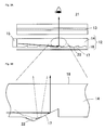
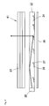
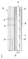
- Fig. 1A shows a schematic sectional view of a structure of a conventional liquid crystal display (see Japanese Patent Gazette No. 3151830 ) and Fig. 1B shows an enlarged view of a part of Fig. 1A.
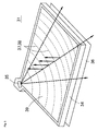
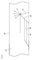
- Fig. 2 shows a schematic perspective view of a back light used in the aforementioned liquid crystal display.
- a liquid crystal display 11 is constituted by overlapping a liquid crystal panel 13 on the surface side of a back light 12.
- the back light 12 is one in which a small light source 15 is arranged at a corner portion of a light guide plate 14 and a reflecting plate 16 is arranged facing the backside of the light guide plate 14.
- Deflection patterns 17, each having a short triangle prism shape arrayed in concentric arcs with a central focus on the position placing the light source 15, are arranged on the backside of the light guide plate 14.
- Such the liquid crystal display 11 has features that electric power consumption is low and brightness is high, because light usability is high. Furthermore, two prism sheets are not required to be disposed between the light emitting plane 18 of the light guide plate 14 and the liquid crystal panel 13 and therefore reduction in thickness and reduction in cost of the liquid crystal display 11 can be achieved.
- the liquid crystal display 11 of such a structure as marked by a dash line shown in Fig. 1 B, when the light reflected at a flat portion of the backside of the light guide plate 14 in the vicinity of the deflection pattern 17 is entered to the deflection pattern 17 and total reflection is performed there, the light is outputted in a direction largely inclined from the direction perpendicular to the light emitting plane 18. As shown in Fig. 2, when the back light 12 is seen from an oblique direction, a bright line 19 is generated on the surface of the light guide plate 14 due to the light to degrade image quality of the liquid crystal display 11.
- Fig. 3A shows a schematic sectional view of a structure of another conventional liquid crystal display and Fig. 3B shows an enlarged view of a part of Fig. 3A.
- a projection 22 having a triangle prism shape is projected on the backside of a light guide plate 14 on the light source side of a deflection pattern 17.
- light incident to the light source side of the deflection pattern 17 is performed by total reflection at the projection 22 to enter to the deflection pattern 17, as marked by a dash line shown in Fig. 3B.
- the light reflected at the deflection pattern 17 is outputted toward a direction substantially perpendicular to a light emitting plane 18 of the light guide plate 14 to be effectively used as illuminated light. Consequently, generation of the bright line 19 as shown in Fig. 2 is suppressed, so that image quality of the liquid crystal display 21 is improved and screen brightness is also improved.
- Embodiments of the present invention provide a surface light source device which is capable of suppressing generation of such aforementioned bright line and is difficult to generate crush of pattern of the backside of a light guide plate even when pressure is applied.
- a surface light source device comprises: a light guide plate having a light emitting plane at one end; and a light source arranged at a corner portion or side of the light guide plate, wherein a plurality of deflection patterns is formed on a plane opposite to the light emitting plane; the deflection pattern outputs light from the light emitting plane by reflecting the light guiding in the light guide plate; a diffusion pattern is formed on the light source side of the deflection pattern; the deflection pattern and the diffusion pattern are formed so as not to protrude outwards of the light guide plate from the plane opposite to the light emitting plane; and the diffusion pattern diffuses the light incident from a light guide direction to a direction different from the light guide direction seen from a direction perpendicular to the light emitting plane.
- the light guide direction denotes a direction connecting the deflection pattern or any position of the light guide plate and the light source in the shortest distance, seen from a direction perpendicular to the light emitting plane of
- a width extending perpendicular to the light guide direction of the diffusion pattern is wider than a width extending perpendicular to the light guide direction of the deflection pattern, when seen from a direction perpendicular to the light emitting plane.
- the diffusion pattern is formed by at least one convex pattern, concave pattern and corrugated pattern.
- the diffusion pattern is a sine wave shape in cross section in a plane perpendicular to the light guide direction and has a uniform cross section in the light guide direction.
- the diffusion pattern is a triangular wave shape in cross section in which an isosceles triangle pattern continues in a plane perpendicular to the light guide direction and has a uniform cross section in the light guide direction.
- the diffusion pattern is a waveform shape in cross section in a plane perpendicular to the light guide direction and has a uniform cross section in the light guide direction; and a pitch of the waveform in cross section perpendicular to the light guide direction is random.
- a pitch in cross section in a plane perpendicular to the light guide direction of the diffusion pattern has the minimum value which is not less than 1.5 ⁇ m and the maximum value which is not less than twice the minimum value; and the diffusion pattern of each pitch in between the minimum value and the maximum value is provided at substantially the same frequency.
- an end placed on the light source side of the diffusion pattern is a shape in which a substantially semi cone shaped pattern is disposed along a direction perpendicular to the light guide direction.
- the diffusion pattern is constituted by a plurality of patterns, each having a hemispheric shape or a semi-elliptical spherical shape.
- the maximum height Rmax of the diffusion pattern is satisfied as follows: 0.2 ⁇ m ⁇ Rmax ⁇ 0.5 ⁇ H, where Rmax is the maximum height of the diffusion pattern measured from the plane opposite to the light emitting plane of the light guide plate; and H is a vertical height of the deflection pattern measured from the plane opposite to the light emitting plane of the light guide plate.
- a length in the light guide direction of the diffusion pattern is not less than twice the length in the light guide direction of an inclined plane which makes the light at the deflection pattern perform total reflection.
- a fine corrugated shape is formed along a ridge line placed at the uppermost portion of the deflection pattern.
- Fig. 1A shows a schematic sectional view of a structure of a liquid crystal display of a prior art 1
- Fig. 1B shows an enlarged view of a part of Fig. 1A;
- Fig. 2 shows a schematic perspective view of a back light used in the liquid crystal display of the prior art 1;
- Fig. 3A shows a schematic sectional view of a structure of a liquid crystal display of a prior art 2
- Fig. 3B shows an enlarged view of a part of Fig. 3A;
- Fig. 4 shows a schematic view for explaining a method for observing crush of a projection formed on the backside of a light guide plate of a liquid crystal display
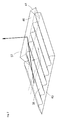
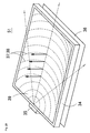
- Fig. 5 shows a perspective view of a surface light source device according to a first embodiment of the present invention
- Fig. 6 shows a schematic plan view of a state where portions of deflection patterns and diffusion patterns are seen from the surface of a light guide plate
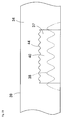
- Fig. 7 shows a perspective view in which a pair of the deflection pattern and the diffusion pattern is seen from the side nearer to a light source situated in the light guide plate;
- Fig. 8 shows an enlarged sectional view of the deflection pattern and the diffusion pattern taken along the X1-X1 line shown in Fig. 6;
- Fig. 9 shows an enlarged sectional view of the deflection pattern and the diffusion pattern taken along the X2-X2 line shown in Fig. 6;
- Fig. 10 shows a view of a relationship between a tilt angle ⁇ 1 (prism tilt angle) of a total reflection plane and a peak angle at which brightness of light outputted from a light emitting plane becomes the maximum;
- Fig. 11 shows a view of a result in which change of brightness of the surface light source device is examined by changing the maximum height Rmax of the diffusion pattern
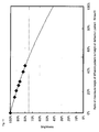
- Fig. 12 shows a view of a relationship between pitch P of the diffusion pattern and a ratio of the zero-order light included in light reflected by the diffusion pattern;
- Fig. 13A, Fig. 13B, and Fig. 13C respectively show views of a directional pattern of light outputted from the light emitting plane of the light guide plate in the prior art 1, the prior art 2, and the first embodiment;
- Fig. 14 shows a view for explaining definition of an elevation angle ⁇ and an azimuthal angle ⁇ used in Fig. 13;
- Fig. 15 shows a view of directional patterns of the prior art 1, the prior art 2, and the first embodiment in a direction parallel to a light guide direction;
- Figs. 16A and 16B show views for explaining an outgoing angle used in Fig. 15, and Fig. 16B shows a sectional view taken along the line X3-X3 shown in Fig. 16A;
- Fig. 17 shows a schematic perspective view of a deflection pattern provided on the backside of a light guide plate and a diffusion pattern in a surface light source device according to a second embodiment of the present invention
- Fig. 18 shows a sectional view taken along the line X4-X4 shown in Fig. 17;
- Fig. 19 shows a view of a relationship between pitch of a diffusion pattern and frequency
- Fig. 20 shows a view of brightness in each outgoing direction of red light (R), green light (G), and blue light (B) diffracted and reflected by the diffusion patterns in the second embodiment;
- Fig. 21 shows a view of brightness in each outgoing direction of red light (R), green light (G), and blue light (B) diffracted and reflected by the diffusion patterns in the first embodiment;
- Fig. 22 shows a schematic perspective view of shapes of a deflection pattern and a diffusion pattern provided on the backside of a light guide plate in a surface light source device according to a third embodiment of the present invention
- Fig. 23 shows a sectional view taken along the line X5-X5 shown in Fig. 22;
- Fig. 24 shows a schematic sectional view for explaining a state in which a bright line is generated by light diffused at a ridge line of the deflection pattern
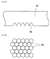
- Fig. 25 shows a cross-sectional view of a different pattern shape of the diffusion pattern
- Fig. 26A shows a cross-sectional view of a further different pattern shape of a diffusion pattern
- Fig. 26B shows a plan view thereof
- Fig. 27A shows a cross-sectional view of a further different pattern shape of a diffusion pattern
- Fig. 27B shows a plan view thereof
- Fig. 28 shows a perspective view for explaining a modification example of a surface light source device
- Fig. 29 shows a perspective view of a surface light source device according to a fourth embodiment of the present invention.
- Fig. 30 shows a perspective view of a liquid crystal display according to a fifth embodiment of the present invention.
- Fig. 31 shows a schematic sectional view of the liquid crystal display according to a fifth embodiment
- Fig. 32 shows a schematic sectional view of a surface light source device provided with a diffusion plate between the surface light source device and the liquid crystal panel;
- Fig. 33 shows a schematic sectional view of a surface light source device provided with a prism sheet between the surface light source device and the liquid crystal panel;
- Fig. 34 shows a view of a mobile telephone according to a sixth embodiment of the present invention.
- Fig. 5 shows a perspective view of a surface light source device according to a first embodiment of the present invention.
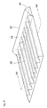
- a surface light source device 31 is one in which a small light source 35 is arranged at a corner portion of a light guide plate 34 made of a transparent resin material and a reflecting plate 36 is arranged facing the backside of the light guide plate 34.
- the light guide plate 34 is molded by a transparent resin material, such as polycarbonate resin, polymethylmethacrylate, and cyclo olefin polymer (referred to as COP).
- a number of fine deflection patterns 37 and fine diffusion patterns 38 are formed on the backside of the light guide plate 34 arrayed in concentric circles with a central focus on the position of the light source 35.
- the deflection patterns 37 and the diffusion patterns 38 are arranged with relatively low density in the vicinity of the light source 35 and arranged with gradually high density with being apart from the light source 35 so that the deflection patterns 37 and the diffusion patterns 38 become substantially uniform in brightness at an effective light emitting region of the surface light source device 31.
- the light source 35 is one in which a bear chip of LED is sealed within a transparent resin and further coated with a white resin at a region except for a light emitting plane thereof. Furthermore, in the example shown in Fig. 5, the light source 35 is fitted at the corner portion situated in the light guide plate 34; however, the light source 35 may be arranged on an outer peripheral portion of the light guide plate 34.
- the reflecting plate 36 is formed by a white sheet or a metal sheet. In addition, when it is referred to as merely the backside of the light guide plate 34, it means the backside of the light guide plate 34, that is, a flat plane opposite to a light emitting plane 39.
- the light guide plate 34 is molded by an injection molding method.
- a molding die is composed of a lower die and an upper die and a molding cavity is formed between the both dies.
- the lower die includes a mirror surface for molding the light emitting plane 39; and the upper die includes a corrugated transcription pattern for molding the deflection pattern 37 and the diffusion pattern 38. Then, melted resin material is injected in the cavity of the molding dies to fill, the resin material is cooled to harden, and then the molding dies are opened to take out the molded light guide plate.
- Fig. 6 shows a schematic plan view of a state where portions of the deflection patterns 37 and the diffusion patterns 38 are seen from the surface of the light guide plate 34.
- Fig. 7 shows a perspective view in which a pair of the deflection pattern 37 and the diffusion pattern 38 is seen from the side nearer to the light source 35 situated in the light guide plate.
- Fig. 8 shows an enlarged sectional view of the deflection pattern 37 and the diffusion pattern 38 taken along the X1-X1 line shown in Fig. 6.
- Fig. 9 shows an enlarged sectional view of the deflection pattern 37 and the diffusion pattern 38 taken along the X2-X2 line shown in Fig. 6.
- the deflection patterns 37 are arranged at spaces each other in concentric circles with a central focus on the position of the light source 35 (alternatively, a virtual light source). In this regard, however, a plurality of deflection patterns 37 is not necessarily required to be placed on one circumference. That is, when seen from a direction perpendicular to the light emitting plane 39 of the light guide plate 34, each of the deflection patterns 37 has its width direction (lengthwise direction) arranged so as to be situated perpendicular to a direction connecting the light source 35 and the aforementioned deflection pattern 37. As shown in Fig. 7 and Fig.
- the deflection pattern 37 is formed by sinking the backside of the light guide plate 34 so as to be triangle prism shape, thereby having a total reflection plane of light 40 placed nearer to the light source 35 and a re-incident plane 41 placed farther from the light source 35.
- the diffusion pattern 38 continues into the deflection pattern 37 and is placed on the side nearer to the light source 35 than the deflection pattern 37.
- the diffusion pattern 38 is provided in a recess 42 partially sunk on the backside of the light guide plate 34 so as not to protrude from the backside of the light guide plate 34.
- the diffusion pattern 38 of this embodiment is a corrugated pattern which makes most part of light beam incident from the light source 35 reflect toward a direction different from a light incident direction thereof, seen from a direction perpendicular to the light emitting plane 39.
- the diffusion pattern 38 is formed in a waveform in cross section and, more particularly, in a form so as to depict in a substantially sine wave, as shown in Fig. 7 and Fig. 9.
- the diffusion pattern 38 changes its height so as to depict a waveform in a direction perpendicular to a light guide direction (in other words, a direction parallel to a direction connecting the light source 35 and the aforementioned diffusion pattern 38, that is, a direction marked by the dash line shown in Fig. 5) and has uniform cross section shape except for both ends in the light guide direction.
- One end of the diffusion pattern 38 is continued into the deflection pattern 37.
- the other end of the diffusion pattern 38 is formed to be an inclined plane 43 having a shape in which a substantially semi cone shaped pattern is disposed along a direction perpendicular to the light guide direction.
- a width of the diffusion pattern 38 is wider than that of the deflection pattern 37; and both ends of the diffusion pattern 38 protrude outward from ends in the width direction of the deflection pattern 37.
- the surface light source device 31 when light is outputted from the light source 35, the light of the light source 35, incident to the inside of the light guide plate 34 goes straight ahead or propagates while repeating total reflection between the surface of the light guide plate 34 and the backside. Then, most of the light is radially propagated with a central focus on substantially the light source 35 when seen from a direction perpendicular to the light emitting plane 39. As marked by a solid arrow shown in Fig. 7 and Fig. 8, the light reached the deflection pattern 37 by propagating within the light guide plate 34 is performed by total reflection at the total reflection plane of light 40 and then outputted toward a substantially vertical direction from the light emitting plane 39.
- an object such as a liquid crystal panel arranged in front of the surface light source device 31 can be vertically illuminated from the backside, whereby a prism sheet, which is provided for aligning the light direction vertically, does not need to be disposed between the surface light source device 31 and the object.
- the surface light source device 31 can also suppress generation of the bright line 19 which has been a problem in the prior art 1 (the surface light source device of Japanese Patent Gazette No. 3151830 ). Furthermore, there is not a possibility that front face brightness of the surface light source device 31 lowers as compared with the prior art 1.
- the diffusion pattern 38 is provided within the recess 42 of the backside of the light guide plate 34 so as not protrude from the backside of the light guide plate 34 and therefore there is not a possibility of damage due to pressure or shock from outside as in the projection 22 of the prior art 2 (the surface light source device of JP-A 2004-045263 ).
- the reflecting plate 36 functions to reenter light leaked from the backside of the light guide plate 34 into the light guide plate 34.
- the re-incident plane 41 functions to catch light leaked from the total reflection plane of light 40 and reenter it into the light guide plate 34. Then, the reflecting plate 36 and the re-incident plane 41 make light usability of the surface light source device 31 improve.
- a tilt angle ⁇ 1 of the total reflection plane 40 ranges from 31 ° to 57° in order to improve light emitting efficiency from the light emitting plane 39.
- Fig. 10 shows a view of a relationship between a tilt angle ⁇ 1 (prism tilt angle) of the total reflection plane of light 40 and a peak angle at which brightness of light outputted from the light emitting plane 39 becomes the maximum.
- a horizontal axis of Fig. 10 shows the tilt angle ⁇ 1 of the total reflection plane of light 40 and a vertical axis shows the peak angle at which the brightness of the light outputted from the light emitting plane 39 becomes the maximum.
- the peak angle denotes an angle measured from a direction including the light guide direction and perpendicular to the light emitting plane 39 in the plane surface perpendicular to the light emitting plane 39.
- the peak angle on the farther side from the light source 35 is shown by a plus value and the peak angle on the nearer to the light source 35 is shown by a plus value.
- the peak angle of the light outputted from the light emitting plane 39 may be set at ranges from -20° to +20°. According to Fig.
- the tilt angle ⁇ 1 of the total reflection plane of light 40 may be set at ranges from 31 ° to 57°. Consequently, if the tilt angle ⁇ 1 of the total reflection plane of light 40 is set at ranges from 31 ° to 57°, the peak angle (angle made in a direction perpendicular to the light emitting plane 39) of the outgoing light of the surface light source device 31 becomes at ranges from -20° to +20°, thereby obtaining good brightness.
- the re-incident plane 41 is kept substantially vertical (tilt angle 90°); however, the re-incident plane 41 is appropriately inclined from the vertical plane in order to facilitate rapping in molding.
- an end of a ridge line of the diffusion pattern 38 is set as a point B'; and an intersection of a vertical line vertically down from the point B' to the backside of the light guide plate 34 and the backside of the light guide plate is set as a point B.
- the light which becomes the bright line 19 in the prior art 1 appears when a light incident to the backside of the light guide plate 34 with being at not less than 20° to the backside of the light guide plate, is performed by total reflection at the backside of the light guide plate and the total reflection plane of light 40. Consequently, in order to suppress generation of the bright line, as marked by the dash line shown in Fig.
- the diffusion pattern 38 may be configured so that light (zero-order reflecting light in the case when the diffusion pattern 38 is considered as a diffraction grating) performed by total reflection at the diffusion pattern 38 is not entered to the total reflection plane of light 40.
- the angle ⁇ 2 may be not more than 20°.
- a projected length W to the backside of the light guide plate of the total reflection plane of light 40 is shown by distance between the point D and a lower end point C of the total reflection plane of light 40.
- a vertical height H of the deflection pattern 37 is expressed by the following equation 1 using the projected length W and the tilt angle ⁇ 1 of the total reflection plane of light 40.
- H W ⁇ tan ⁇ ⁇ 1
- L distance between the lower end point C of the total reflection plane of light 40 and the point B (referred to as a length of the diffusion pattern 38 below)
- H W + L ⁇ tan ⁇ ⁇ 2 Consequently, condition that ⁇ 2 is not less than 20°can be obtained by the following equation 3 from the aforementioned equation 1 and equation 2.
- L W ⁇ tan ⁇ ⁇ 1 / tan 20 ° ⁇ 1
- the vertical height H of the deflection pattern 37 is equal to the projected length W of the total reflection plane of light 40. Then the following equation can be obtained from the aforementioned equation 3. L > 1.75 ⁇ W Consequently, the length L of the diffusion pattern 38 can be more than about twice the projected length W of the total reflection plane of light 40 if some amount of margin is provided. Since the projected length W of the total reflection plane of light 40 is usually approximately 5 ⁇ m, the vertical height H of the deflection pattern 37 is also approximately 5 ⁇ m and therefore the length L of the diffusion pattern 38 may be not less than about 10 ⁇ m.
- a project area to the backside of the light guide plate of the diffusion pattern 38 may be not less than about twice the project area to the backside of the light guide plate of the total reflection plane of light 40. Furthermore, if area of the diffusion pattern 38 is excess, light diffusion becomes large and therefore in several embodiments the width of the diffusion pattern 38 is smaller than "W + Pmax".
- the length L of the diffusion pattern 38 is not less than about twice the projected length W of the total reflection plane of light 40 and therefore light incident to the diffusion pattern 38 at an angle of more than 20° is reflected at the total thereby preventing the light from becoming bright line to suppress generation of the bright line.
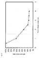
- Fig. 11 shows a view of a result in which change of brightness of the surface light source device 31 is examined by changing the maximum height Rmax of the diffusion pattern 38.
- a horizontal axis of Fig. 11 shows a ratio of the maximum height Rmax of the diffusion pattern 38 with respect to the vertical height H of the deflection pattern 37 and a vertical axis shows brightness ratio of the surface light source device 31.
- brightness ratio makes brightness when the diffusion pattern 38 is not provided set as 100%. Decreasing rate of the permissible brightness is approximately 25% when the diffusion pattern 38 is not provided; and it turns out that this is Rmax/H ⁇ 0.5 according to Fig. 11. Consequently, this may be set as Rmax ⁇ 0.5H.
- an angle made by a light line direction of the light guiding in the light guide plate 34 with respect to the backside of the light guide plate 34 is within ranges from -40° to +40°.
- the diffusion pattern 38 functions as a reflective diffraction grating and therefore if the diffusion pattern 38 having a size in which light of such the angle region does not diffract at the diffusion pattern 38 is made, zero order light (specular reflection light) of the light reflected at the diffusion pattern 38 increases to cause generation of the bright line.
- the maximum height Rmax of the diffusion pattern needs not less than 0.2 ⁇ m in order that the light diffracts at the diffusion pattern 38. Consequently, a lower limit of the maximum height Rmax of the diffusion pattern 38 is 0.2 ⁇ m and the range of the maximum height Rmax of the diffusion pattern 38 becomes the following as described above (equation 4). 0.2 ⁇ m ⁇ R ⁇ max ⁇ 0.5 ⁇ H
- difference in height of the crests and troughs of the corrugated diffusion pattern 38 is as much as possible approximately equal to Rmax.
- pitch (cycle) P of the diffusion pattern 38 shown in Fig. 9 is preferable to be not less than 1.5 ⁇ m.
- the pitch of the diffusion pattern 38 denotes a horizontal distance between adjacent projections (the maximum position) as shown in Fig. 9.
- a ratio of the zero-order (diffraction) light changes depending on the pitch P of the diffusion pattern 38 as shown in Fig. 12.
- the number of the bright lines can be decreased if the ratio of the zero order light is set so as to be not more than 50% and therefore it turns out that the pitch P of the diffusion pattern 38 may be not less than 1.5 ⁇ m according to Fig. 12.
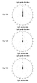
- Fig. 13A, Fig. 13B, and Fig. 13C respectively show views of a directional pattern of light outputted from the light emitting plane of the light guide plate in the prior art 1, the prior art 2, and the first embodiment; and a it shows that the deeper the color is, the higher the brightness is.
- the center of each circle denotes a direction perpendicular to the light emitting plane of the light guide plate; distance (radius) from the center denotes an elevation angle ⁇ measured from a direction perpendicular to the light emitting plane; and circumferential angle denotes an azimuthal angle ⁇ in which the light guide direction is set as the standard.
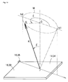
- Fig. 14 shows a view for explaining definition of the elevation angle ⁇ and the azimuthal angle ⁇ used in Fig. 13.
- a point F denotes an any position in the light emitting plane 18 or 39 of the light guide plate 14 or 34; and a dashed-dotted line FG denotes a vertical line stood on the light emitting planes 18 and 39.
- a thick solid arrow K denotes an outgoing direction vector showing an outgoing direction of light outputted from the point F.
- an angle made by the vertical line FG and the outgoing direction vector K denotes the elevation angle ⁇ .
- a circle M with a central focus on the point G, coming in contact with the outgoing direction vector K, and parallel to the light emitting plane 18 or 39, is considered.
- a plane including a line segment connecting the light source 15 or 35 and the point F and the vertical line FG is assumed; and of two intersections of the plane and the circle M, a point of light guide direction (a farther side from the light source) is set as N1, and a point of a light source direction (a nearer side to the light source) is set as N2. Furthermore, a contact point of the circle M and the outgoing direction vector K is set as Q. Then, an angle measured in counterclockwise rotation from a GN1 direction to a GQ direction is an azimuthal angle ⁇ . Put simply, seen from a direction perpendicular to the light emitting plane 18 or 39, an angle measured in counterclockwise rotation from the light guide direction to the light emitting direction is an azimuthal angle ⁇ (refer to Fig. 16).
- the outgoing light extends long in the light guide direction and this becomes the bright line.
- the outgoing light gathers at the central portion (in the vicinity of a direction a perpendicular to the light emitting plane) to suppress generation of the bright line.
- Fig. 15 shows a view of directional patterns of the prior art 1 (symbol: 0), the prior art 2 (symbol: ⁇ ), and the first embodiment (symbol: •) in the direction parallel to the light guide direction.
- a horizontal axis in Fig. 15 shows an outgoing angle of light in the light guide direction.
- the outgoing angle of the light in the light guide direction is an outgoing angle in the plane perpendicular to the light emitting plane including the light guide direction shown in Fig. 16B as the X3-X3 cross section of Fig. 16A. This is equal to the elevation angle ⁇ when the azimuthal angle ⁇ is 0° and 180°.
- Fig. 15 shows a view of directional patterns of the prior art 1 (symbol: 0), the prior art 2 (symbol: ⁇ ), and the first embodiment (symbol: •) in the direction parallel to the light guide direction.
- a horizontal axis in Fig. 15 shows an outgoing angle of light
- the brightness in the region which becomes the bright line is high and therefore the bright line 19 as shown in Fig. 2 is generated.
- the brightness becomes small equal to the prior art 2 in the region which becomes the bright line and consequently the bright line can be suppressed to the level equal to the prior art 2.
- the brightness of the first embodiment becomes a little bit smaller than that of the prior art 2; however, it becomes the brightness equal to the prior art 1.
- the surface light source device of the first embodiment it turns out that degradation of image quality due to the bright line can be solved without degrading the front face brightness, as compared with the surface light source device of the prior art 1.
- damage of the pattern is generated in the prior art 2, however, damage of the pattern is not generated in the surface light source devices of the prior art 1 and the first embodiment.
- Fig. 17 shows a schematic perspective view of a deflection pattern 37 and a diffusion pattern 38 provided on the backside of a light guide plate in a surface light source device according to a second embodiment. Furthermore, Fig. 18 shows a view of a cross section of the diffusion pattern 38 and a sectional view taken along the line X4-X4 shown in Fig. 17.
- one incorporating a tricolor LED with red green and blue colors is used as a light source 35. Then, red light, green light, and blue light are mixed to generate white light.
- a diffusion pattern 38 is of a substantially sine wave shape in cross section; however, horizontal distance between sine wave shaped adjacent projections (pitch P of the diffusion pattern 38) is not constant but changes in a random manner.
- the minimum value Pmin of the pitch P of the diffusion pattern 38 is not less than 1.5 ⁇ m and the maximum value Pmax of the pitch P of the diffusion pattern 38 is a size of not less than twice the minimum value.
- the minimum value Pmin of the pitch P of the diffusion pattern 38 is 2.5 ⁇ m and the maximum value Pmax of the pitch P of the diffusion pattern 38 is 5 ⁇ m.
- the reason why the minimum value Pmin of the pitch P of the diffusion pattern 38 is not less than 1.5 ⁇ m is to set the ratio of the zero order light included in the light reflected at the diffusion pattern 38 to be not more than 50%, as described in Fig. 12.
- the pitches P of the diffusion patterns 38 are random, the pitches P between the adjacent projections of the diffusion patterns 38 formed in a random manner are formed so as to be appeared in the light guide plate at a substantially the same frequency. That is, when the diffusion patterns 38 formed on the whole of the light guide plate 34 or the diffusion pattern 38 formed in any part region of the light guide plate 34 are considered, as shown in Fig. 19, the diffusion patterns 38 disposed for each pitch P are included each other in the same number (frequency). Therefore, light diffusion state by the diffusion patterns 38 becomes substantially uniform on the whole of the light guide plate 34, so that uneven brightness is difficult to be generated in the light guide plate 34.
- Fig. 20 shows brightness in each outgoing direction of red light (R), green light (G), and blue light (B) diffracted and reflected by the diffusion patterns 38 in the second embodiment having the diffusion pattern 38 with random pitches.
- Fig. 21 shows brightness in each outgoing direction of red light (R), green light (G), and blue light (B) diffracted and reflected by the diffusion patterns 38 in the first embodiment having the diffusion pattern 38 with a constant pitch.
- the light source uses a white light source of mixed type composed of red light, green light, and blue light in the surface light source device having the diffusion pattern 38 with a constant pitch; as shown in Fig.
- diffracted light (diffracted light except for zero order light) reflected at the diffusion pattern 38 generate color shift and the light emitting plane of the surface light source device seems to be colored like a rainbow.
- diffracted light other than the zero order light reduces by half, decreases color separation at the light emitting plane, and the degree of color mixture of red light, green light, and blue light is enhanced to be able to output white light from the light emitting plane.
- the optimum value example and design conditions described in the first embodiment can be applicable.
- Fig. 22 shows a schematic perspective view of shapes of a deflection pattern 37 and a diffusion pattern 38 provided on the backside of a light guide plate in a surface light source device according to a third embodiment of the present invention.
- Fig. 23 shows a view of a cross section of the diffusion pattern 38 and a sectional view taken along the line X5-X5 shown in Fig. 22.
- a fine corrugated pattern 44 is formed along a ridge line of the deflection pattern 37 (the highest position: a point D' in cross section).
- a sine wave shape pattern is exemplified in the drawing; however, a different pattern may be used.
- a pitch of the corrugated pattern 44 is equal to a pitch P of the diffusion pattern 38.
- the maximum height Rmax of the diffusion pattern 38 and the maximum difference of elevation Rmax2 of the corrugated pattern 44 are set as the following equation 4. 0.2 ⁇ m ⁇ R ⁇ max + R ⁇ max ⁇ 2 ⁇ 0.5 ⁇ H where, H is a vertical height of the deflection pattern 37.
- the ridge line of the deflection pattern 37 is not formed at a sharp angle when forming the light guide plate 34 and the ridge line of the deflection pattern 37 is rounded due to filling defect of resin. Therefore, as shown in Fig. 24, light incident to the ridge line of the deflection pattern 37 is scattered within the vertical plane of the light guide direction due to the rounded ridge line of the deflection pattern 37 to cause generation of the bright line on the light emitting plane 39.
- the corrugated pattern 44 is formed along the ridge line of the deflection pattern 37 and therefore the light incident to the ridge line of the deflection pattern 37 is scattered not only to within the vertical plane of the light guide direction but also to a direction out of the vertical plane.
- the light reflected at the ridge line of the deflection pattern 37 is also scattered to lateral directions with respect to the light guide direction.
- generation of the bright line at the light emitting plane 39 can be effectively suppressed.
- the diffusion patterns 38 having a sine wave shaped cross section are described; however, as shown in Fig. 25, a diffusion pattern 38 may have a cross section of a triangular wave shape in which a substantially isosceles triangle pattern is continuously repeated.
- the maximum height Rmax of the diffusion pattern 38 is set as the following equation. 0.2 ⁇ m ⁇ R ⁇ max ⁇ 0.5 ⁇ H (where, H is the height of the deflection pattern 37)
- the diffusion pattern 38 does not need to be a rod-like shape extending in the light guide direction; however, it may be one in which a quaquaversal pattern such as a hemispheric or a semi-elliptical spherical shaped pattern is arranged almost without clearance, as shown in Figs. 26A and 26B, for example. Furthermore, as shown in Figs. 27A and 27B, it may be one in which a cone shaped, an elliptical cone shaped, a pyramid shaped, or a square pyramid shaped pattern is arranged without clearance.
- Fig. 28 shows a perspective view of a surface light source device 51 in which a light source 35 is arranged at the central portion of one side of a light guide plate 34.
- the light source 35 is arranged at a corner portion of the light guide plate 34 in the first embodiment; however, the light source 35 maybe arranged at the central portion of the one side of the light guide plate 34 as shown in Fig. 28.
- a light guide direction is a direction connecting the light source 35 and deflection patterns 37; each of the deflection patterns 37 is arranged so that its width direction intersects with the light guide direction; and a diffusion pattern 38 changes cross section shape (pattern) along a direction intersecting to the light guide direction.
- Fig. 29 shows a perspective view of a surface light source device 52 according to a forth embodiment in which a light source 35 is arranged along one side of a light guide plate 34.
- the surface light source device 52 includes the light source 35 (a linear light source), which is substantially extended over the whole length of one side of the light guide plate 34.
- Deflection patterns 37 and diffusion patterns 38 are formed on the backside of the light guide plate 34.
- a light guide direction denotes a direction connecting each of the deflection patterns 37 and the light source 35 in the shortest distance; and it means a direction marked by a dash line shown in Fig. 29 in the surface light source device 52; that is, a direction perpendicular to a lengthwise direction of the light source 35, seen from a direction perpendicular to the light emitting plane 39. It defines that the light guide direction is the direction connecting each of the deflection patterns 37 and the light source 35 in the case of the small light source 35 (a point light source) shown in Fig. 5; however, new definition that "the light guide direction is the direction connecting each of the deflection patterns 37 and the light source 35 in the shortest distance" is one which extends the former definition and includes the former definition.
- the deflection pattern 37 is formed in a triangular shaped cross section in a cross section along the light guide direction and extends in a uniform cross section along a direction intersecting to the light guide direction. Furthermore, pitch in the length direction of the light guide plate 34 shortens with being farther from the light source 35.
- the diffusion pattern 38 is arranged on the side of the light source 35 side of the each deflection pattern 37; a pattern in cross section changes in a sine wave shape in a direction perpendicular to the light guide direction and extends in a uniform cross section in a direction parallel to the light guide direction.
- Fig. 30 shows a perspective view of a liquid crystal display 61 provided with a surface light source device 32 according to a fifth embodiment of the present invention.
- Fig. 31 shows a schematic sectional view of the aforementioned liquid crystal display 61. That is, a liquid crystal panel 33 is arranged in front of the surface light source device 32. In such the liquid crystal display 61, the liquid crystal panel 33 can be vertically illuminated from the backside by the surface light source device 32 without using a prism panel or the like. Then, the bright line is not generated in the liquid crystal display 61 and image visibility is improved by using the surface light source device 32 according to the present invention. In addition, there is not a possibility to damage the diffusion pattern 38 by external force and shock.
- a diffusion plate 63 may be sandwiched between the surface light source device 32 and the liquid crystal panel 33 as shown in Fig. 32, if needed.
- the outgoing light may be steered to the vertical direction by sandwiching a prism sheet 64 between the surface light source device 32 and the liquid crystal panel 33.
- a liquid crystal display it is not limited to a back light type in which the liquid crystal panel is illuminated from a side (the backside side) opposite to an observer; however, a front light type in which the liquid crystal panel is illuminated from an observer side (the front side) may be used. Furthermore, a reversible light in which the image can be observed from both sides by means of one sheet of the surface light source device and one sheet of the liquid crystal panel may be used.
- Fig. 34 shows a view of an example of use of a liquid crystal display according to one aspect of the present invention.
- Fig. 34 shows a flip mobile telephone 71.
- the mobile telephone 71 is composed of an operation unit 72 and a display unit 73.
- the operation unit 72 includes an operation key 77 such as a numeric keypad or the like and a microphone 76.
- the display unit 73 includes a liquid crystal display 74 and a speaker 75.
- the light source can be incorporated so as to be placed at any direction in the liquid crystal display 74.
- the liquid crystal display 74 may be a double-side display type.
- the mobile telephone 71 can be easily watched because of no generation of the bright line.
- PDA personal digital assistant
Landscapes
- Physics & Mathematics (AREA)
- General Physics & Mathematics (AREA)
- Optics & Photonics (AREA)
- Nonlinear Science (AREA)
- Mathematical Physics (AREA)
- Chemical & Material Sciences (AREA)
- Crystallography & Structural Chemistry (AREA)
- Planar Illumination Modules (AREA)
- Light Guides In General And Applications Therefor (AREA)
- Liquid Crystal (AREA)
Abstract
Each of the diffusing elements consists of a recess having an undulating ribbed surface (fig 7), such that the profile of the recess perpendicular to the direction of incident light (43) exhibits a wave-like form in the recess depth. The ribs run substantially parallel to the direction of incident light exhibiting a substantially uniform rectangular profile in that direction.
Description
- The present invention relates to a surface light source device and, more particularly, to a surface light source device used as a back light, a front light, and a reversible light, for use in a liquid crystal display.
- Fig. 1A shows a schematic sectional view of a structure of a conventional liquid crystal display (see Japanese Patent Gazette
No. 3151830 - A
liquid crystal display 11 is constituted by overlapping aliquid crystal panel 13 on the surface side of aback light 12. Theback light 12 is one in which asmall light source 15 is arranged at a corner portion of alight guide plate 14 and a reflectingplate 16 is arranged facing the backside of thelight guide plate 14.Deflection patterns 17, each having a short triangle prism shape arrayed in concentric arcs with a central focus on the position placing thelight source 15, are arranged on the backside of thelight guide plate 14. - Therefore, when the
light source 15 is emitted, light of thelight source 15 incident from a light incident surface of thelight guide plate 14 to the inside of thelight guide plate 14 is radially propagated in thelight guide plate 14 while total reflection is repeated between the surface (light emitting plane 18) of thelight guide plate 14 and the backside. Light incident to thedeflection pattern 17 on this midstream is performed by total reflection at thedeflection pattern 17, as marked by a solid arrow shown in Fig. 1A and Fig. 1B. The light performed by total reflection is outputted substantially vertically from thelight emitting plane 18 to outside to illuminate theliquid crystal panel 13 from the backside side. - Such the
liquid crystal display 11 has features that electric power consumption is low and brightness is high, because light usability is high. Furthermore, two prism sheets are not required to be disposed between thelight emitting plane 18 of thelight guide plate 14 and theliquid crystal panel 13 and therefore reduction in thickness and reduction in cost of theliquid crystal display 11 can be achieved. - However, in the
liquid crystal display 11 of such a structure, as marked by a dash line shown in Fig. 1 B, when the light reflected at a flat portion of the backside of thelight guide plate 14 in the vicinity of thedeflection pattern 17 is entered to thedeflection pattern 17 and total reflection is performed there, the light is outputted in a direction largely inclined from the direction perpendicular to thelight emitting plane 18. As shown in Fig. 2, when theback light 12 is seen from an oblique direction, abright line 19 is generated on the surface of thelight guide plate 14 due to the light to degrade image quality of theliquid crystal display 11. - Fig. 3A shows a schematic sectional view of a structure of another conventional liquid crystal display and Fig. 3B shows an enlarged view of a part of Fig. 3A. In order to solve the aforementioned problem, in a
liquid crystal display 21 disclosed inJapanese Patent Application No. 2004-045263 projection 22 having a triangle prism shape is projected on the backside of alight guide plate 14 on the light source side of adeflection pattern 17. When such theprojection 22 is provided, light incident to the light source side of thedeflection pattern 17 is performed by total reflection at theprojection 22 to enter to thedeflection pattern 17, as marked by a dash line shown in Fig. 3B. As a result, the light reflected at thedeflection pattern 17 is outputted toward a direction substantially perpendicular to alight emitting plane 18 of thelight guide plate 14 to be effectively used as illuminated light. Consequently, generation of thebright line 19 as shown in Fig. 2 is suppressed, so that image quality of theliquid crystal display 21 is improved and screen brightness is also improved. - However, in the method in which the
projection 22 of the triangle prism shape is projected on the backside of thelight guide plate 14, there arises a problem in that when pressure is applied from the reflectingplate 16 side of the backside of thelight guide plate 14, theprojection 22 is crashed due to the pressure. For example, as shown in Fig. 4, when theliquid crystal display 21 is reversed and is pressed by ametallic rod 23 from above the reflectingplate 16, crush of theprojection 22 is observed. During assembly or use of theliquid crystal display 21, there is a case that theliquid crystal display 21 is dropped, and in this case, there is a possibility that theprojection 22 of thelight guide plate 14 is crushed. Consequently, there is a possibility that brightness decreases at the crushed point of theprojection 22 and a bright line is generated. In addition,reference numeral 24 shown in Fig. 4 denotes a diffusion plate. - Embodiments of the present invention provide a surface light source device which is capable of suppressing generation of such aforementioned bright line and is difficult to generate crush of pattern of the backside of a light guide plate even when pressure is applied.
- In accordance with one aspect of the present invention, a surface light source device comprises: a light guide plate having a light emitting plane at one end; and a light source arranged at a corner portion or side of the light guide plate, wherein a plurality of deflection patterns is formed on a plane opposite to the light emitting plane; the deflection pattern outputs light from the light emitting plane by reflecting the light guiding in the light guide plate; a diffusion pattern is formed on the light source side of the deflection pattern; the deflection pattern and the diffusion pattern are formed so as not to protrude outwards of the light guide plate from the plane opposite to the light emitting plane; and the diffusion pattern diffuses the light incident from a light guide direction to a direction different from the light guide direction seen from a direction perpendicular to the light emitting plane. In addition, the light guide direction denotes a direction connecting the deflection pattern or any position of the light guide plate and the light source in the shortest distance, seen from a direction perpendicular to the light emitting plane of the light guide plate.
- An embodiment of the present invention, a width extending perpendicular to the light guide direction of the diffusion pattern is wider than a width extending perpendicular to the light guide direction of the deflection pattern, when seen from a direction perpendicular to the light emitting plane.
- An embodiment of the present invention, the diffusion pattern is formed by at least one convex pattern, concave pattern and corrugated pattern.
- An embodiment of the present invention, the diffusion pattern is a sine wave shape in cross section in a plane perpendicular to the light guide direction and has a uniform cross section in the light guide direction.
- An embodiment of the present invention, the diffusion pattern is a triangular wave shape in cross section in which an isosceles triangle pattern continues in a plane perpendicular to the light guide direction and has a uniform cross section in the light guide direction.
- An embodiment of the present invention, the diffusion pattern is a waveform shape in cross section in a plane perpendicular to the light guide direction and has a uniform cross section in the light guide direction; and a pitch of the waveform in cross section perpendicular to the light guide direction is random.
- An embodiment of the present invention, a pitch in cross section in a plane perpendicular to the light guide direction of the diffusion pattern has the minimum value which is not less than 1.5µm and the maximum value which is not less than twice the minimum value; and the diffusion pattern of each pitch in between the minimum value and the maximum value is provided at substantially the same frequency.
- An embodiment of the present invention, an end placed on the light source side of the diffusion pattern is a shape in which a substantially semi cone shaped pattern is disposed along a direction perpendicular to the light guide direction.
- An embodiment of the present invention, the diffusion pattern is constituted by a plurality of patterns, each having a hemispheric shape or a semi-elliptical spherical shape.
- An embodiment of the present invention, the maximum height Rmax of the diffusion pattern is satisfied as follows: 0.2µm≤Rmax≤0.5×H,
where Rmax is the maximum height of the diffusion pattern measured from the plane opposite to the light emitting plane of the light guide plate; and H is a vertical height of the deflection pattern measured from the plane opposite to the light emitting plane of the light guide plate. - An embodiment of the present invention, a length in the light guide direction of the diffusion pattern is not less than twice the length in the light guide direction of an inclined plane which makes the light at the deflection pattern perform total reflection.
- An embodiment of the present invention, a fine corrugated shape is formed along a ridge line placed at the uppermost portion of the deflection pattern.
- In addition, the above-described constituent elements and embodiments of the present invention can be arbitrarily combined as much as possible.
- Fig. 1A shows a schematic sectional view of a structure of a liquid crystal display of a
prior art 1, and Fig. 1B shows an enlarged view of a part of Fig. 1A; - Fig. 2 shows a schematic perspective view of a back light used in the liquid crystal display of the
prior art 1; - Fig. 3A shows a schematic sectional view of a structure of a liquid crystal display of a
prior art 2, and Fig. 3B shows an enlarged view of a part of Fig. 3A; - Fig. 4 shows a schematic view for explaining a method for observing crush of a projection formed on the backside of a light guide plate of a liquid crystal display;
- Fig. 5 shows a perspective view of a surface light source device according to a first embodiment of the present invention;
- Fig. 6 shows a schematic plan view of a state where portions of deflection patterns and diffusion patterns are seen from the surface of a light guide plate;
- Fig. 7 shows a perspective view in which a pair of the deflection pattern and the diffusion pattern is seen from the side nearer to a light source situated in the light guide plate;
- Fig. 8 shows an enlarged sectional view of the deflection pattern and the diffusion pattern taken along the X1-X1 line shown in Fig. 6;
- Fig. 9 shows an enlarged sectional view of the deflection pattern and the diffusion pattern taken along the X2-X2 line shown in Fig. 6;
- Fig. 10 shows a view of a relationship between a tilt angle θ1 (prism tilt angle) of a total reflection plane and a peak angle at which brightness of light outputted from a light emitting plane becomes the maximum;
- Fig. 11 shows a view of a result in which change of brightness of the surface light source device is examined by changing the maximum height Rmax of the diffusion pattern;
- Fig. 12 shows a view of a relationship between pitch P of the diffusion pattern and a ratio of the zero-order light included in light reflected by the diffusion pattern;
- Fig. 13A, Fig. 13B, and Fig. 13C respectively show views of a directional pattern of light outputted from the light emitting plane of the light guide plate in the
prior art 1, theprior art 2, and the first embodiment; - Fig. 14 shows a view for explaining definition of an elevation angle ξ and an azimuthal angle ζ used in Fig. 13;
- Fig. 15 shows a view of directional patterns of the
prior art 1, theprior art 2, and the first embodiment in a direction parallel to a light guide direction; - Figs. 16A and 16B show views for explaining an outgoing angle used in Fig. 15, and Fig. 16B shows a sectional view taken along the line X3-X3 shown in Fig. 16A;
- Fig. 17 shows a schematic perspective view of a deflection pattern provided on the backside of a light guide plate and a diffusion pattern in a surface light source device according to a second embodiment of the present invention;
- Fig. 18 shows a sectional view taken along the line X4-X4 shown in Fig. 17;
- Fig. 19 shows a view of a relationship between pitch of a diffusion pattern and frequency;
- Fig. 20 shows a view of brightness in each outgoing direction of red light (R), green light (G), and blue light (B) diffracted and reflected by the diffusion patterns in the second embodiment;
- Fig. 21 shows a view of brightness in each outgoing direction of red light (R), green light (G), and blue light (B) diffracted and reflected by the diffusion patterns in the first embodiment;
- Fig. 22 shows a schematic perspective view of shapes of a deflection pattern and a diffusion pattern provided on the backside of a light guide plate in a surface light source device according to a third embodiment of the present invention;
- Fig. 23 shows a sectional view taken along the line X5-X5 shown in Fig. 22;
- Fig. 24 shows a schematic sectional view for explaining a state in which a bright line is generated by light diffused at a ridge line of the deflection pattern;
- Fig. 25 shows a cross-sectional view of a different pattern shape of the diffusion pattern;
- Fig. 26A shows a cross-sectional view of a further different pattern shape of a diffusion pattern, and Fig. 26B shows a plan view thereof;
- Fig. 27A shows a cross-sectional view of a further different pattern shape of a diffusion pattern, and Fig. 27B shows a plan view thereof;
- Fig. 28 shows a perspective view for explaining a modification example of a surface light source device;
- Fig. 29 shows a perspective view of a surface light source device according to a fourth embodiment of the present invention;
- Fig. 30 shows a perspective view of a liquid crystal display according to a fifth embodiment of the present invention;
- Fig. 31 shows a schematic sectional view of the liquid crystal display according to a fifth embodiment;
- Fig. 32 shows a schematic sectional view of a surface light source device provided with a diffusion plate between the surface light source device and the liquid crystal panel;
- Fig. 33 shows a schematic sectional view of a surface light source device provided with a prism sheet between the surface light source device and the liquid crystal panel; and
- Fig. 34 shows a view of a mobile telephone according to a sixth embodiment of the present invention.
- Embodiments according to the present invention will be described below in detail with reference to the drawings.
- Fig. 5 shows a perspective view of a surface light source device according to a first embodiment of the present invention. As shown in Fig. 5, a surface
light source device 31 is one in which a smalllight source 35 is arranged at a corner portion of alight guide plate 34 made of a transparent resin material and a reflectingplate 36 is arranged facing the backside of thelight guide plate 34. Thelight guide plate 34 is molded by a transparent resin material, such as polycarbonate resin, polymethylmethacrylate, and cyclo olefin polymer (referred to as COP). A number offine deflection patterns 37 andfine diffusion patterns 38 are formed on the backside of thelight guide plate 34 arrayed in concentric circles with a central focus on the position of thelight source 35. Thedeflection patterns 37 and thediffusion patterns 38 are arranged with relatively low density in the vicinity of thelight source 35 and arranged with gradually high density with being apart from thelight source 35 so that thedeflection patterns 37 and thediffusion patterns 38 become substantially uniform in brightness at an effective light emitting region of the surfacelight source device 31. Thelight source 35 is one in which a bear chip of LED is sealed within a transparent resin and further coated with a white resin at a region except for a light emitting plane thereof. Furthermore, in the example shown in Fig. 5, thelight source 35 is fitted at the corner portion situated in thelight guide plate 34; however, thelight source 35 may be arranged on an outer peripheral portion of thelight guide plate 34. The reflectingplate 36 is formed by a white sheet or a metal sheet. In addition, when it is referred to as merely the backside of thelight guide plate 34, it means the backside of thelight guide plate 34, that is, a flat plane opposite to alight emitting plane 39. - The
light guide plate 34 is molded by an injection molding method. In other words, a molding die is composed of a lower die and an upper die and a molding cavity is formed between the both dies. The lower die includes a mirror surface for molding thelight emitting plane 39; and the upper die includes a corrugated transcription pattern for molding thedeflection pattern 37 and thediffusion pattern 38. Then, melted resin material is injected in the cavity of the molding dies to fill, the resin material is cooled to harden, and then the molding dies are opened to take out the molded light guide plate. - Fig. 6 shows a schematic plan view of a state where portions of the
deflection patterns 37 and thediffusion patterns 38 are seen from the surface of thelight guide plate 34. Fig. 7 shows a perspective view in which a pair of thedeflection pattern 37 and thediffusion pattern 38 is seen from the side nearer to thelight source 35 situated in the light guide plate. Fig. 8 shows an enlarged sectional view of thedeflection pattern 37 and thediffusion pattern 38 taken along the X1-X1 line shown in Fig. 6. Fig. 9 shows an enlarged sectional view of thedeflection pattern 37 and thediffusion pattern 38 taken along the X2-X2 line shown in Fig. 6. - As shown in Fig. 6, the
deflection patterns 37 are arranged at spaces each other in concentric circles with a central focus on the position of the light source 35 (alternatively, a virtual light source). In this regard, however, a plurality ofdeflection patterns 37 is not necessarily required to be placed on one circumference. That is, when seen from a direction perpendicular to thelight emitting plane 39 of thelight guide plate 34, each of thedeflection patterns 37 has its width direction (lengthwise direction) arranged so as to be situated perpendicular to a direction connecting thelight source 35 and theaforementioned deflection pattern 37. As shown in Fig. 7 and Fig. 8, thedeflection pattern 37 is formed by sinking the backside of thelight guide plate 34 so as to be triangle prism shape, thereby having a total reflection plane of light 40 placed nearer to thelight source 35 and are-incident plane 41 placed farther from thelight source 35. - The
diffusion pattern 38 continues into thedeflection pattern 37 and is placed on the side nearer to thelight source 35 than thedeflection pattern 37. Thediffusion pattern 38 is provided in arecess 42 partially sunk on the backside of thelight guide plate 34 so as not to protrude from the backside of thelight guide plate 34. Thediffusion pattern 38 of this embodiment is a corrugated pattern which makes most part of light beam incident from thelight source 35 reflect toward a direction different from a light incident direction thereof, seen from a direction perpendicular to thelight emitting plane 39. In this embodiment described here, thediffusion pattern 38 is formed in a waveform in cross section and, more particularly, in a form so as to depict in a substantially sine wave, as shown in Fig. 7 and Fig. 9. Thediffusion pattern 38 changes its height so as to depict a waveform in a direction perpendicular to a light guide direction (in other words, a direction parallel to a direction connecting thelight source 35 and theaforementioned diffusion pattern 38, that is, a direction marked by the dash line shown in Fig. 5) and has uniform cross section shape except for both ends in the light guide direction. One end of thediffusion pattern 38 is continued into thedeflection pattern 37. The other end of thediffusion pattern 38 is formed to be aninclined plane 43 having a shape in which a substantially semi cone shaped pattern is disposed along a direction perpendicular to the light guide direction. A width of thediffusion pattern 38 is wider than that of thedeflection pattern 37; and both ends of thediffusion pattern 38 protrude outward from ends in the width direction of thedeflection pattern 37. - Therefore, in the surface
light source device 31, when light is outputted from thelight source 35, the light of thelight source 35, incident to the inside of thelight guide plate 34 goes straight ahead or propagates while repeating total reflection between the surface of thelight guide plate 34 and the backside. Then, most of the light is radially propagated with a central focus on substantially thelight source 35 when seen from a direction perpendicular to thelight emitting plane 39. As marked by a solid arrow shown in Fig. 7 and Fig. 8, the light reached thedeflection pattern 37 by propagating within thelight guide plate 34 is performed by total reflection at the total reflection plane oflight 40 and then outputted toward a substantially vertical direction from thelight emitting plane 39. Therefore, an object such as a liquid crystal panel arranged in front of the surfacelight source device 31 can be vertically illuminated from the backside, whereby a prism sheet, which is provided for aligning the light direction vertically, does not need to be disposed between the surfacelight source device 31 and the object. - Furthermore, the light reached the
diffusion pattern 38 is diffused to the right and the left depending on thediffusion pattern 38, as marked by dash lines shown in Fig. 7, 8 and 9. Consequently, the light reflected at thediffusion pattern 38 or the light reflected at thediffusion pattern 38 and further reflected at the total reflection plane oflight 40 is emitted toward a direction out of the direction of thebright line 19 shown in Fig. 2 and the outgoing direction is not also uniformed. Therefore, the surfacelight source device 31 can also suppress generation of thebright line 19 which has been a problem in the prior art 1 (the surface light source device of Japanese Patent GazetteNo. 3151830 light source device 31 lowers as compared with theprior art 1. - Furthermore, the
diffusion pattern 38 is provided within therecess 42 of the backside of thelight guide plate 34 so as not protrude from the backside of thelight guide plate 34 and therefore there is not a possibility of damage due to pressure or shock from outside as in theprojection 22 of the prior art 2 (the surface light source device ofJP-A 2004-045263 - In addition, the reflecting
plate 36 functions to reenter light leaked from the backside of thelight guide plate 34 into thelight guide plate 34. There-incident plane 41 functions to catch light leaked from the total reflection plane oflight 40 and reenter it into thelight guide plate 34. Then, the reflectingplate 36 and there-incident plane 41 make light usability of the surfacelight source device 31 improve. - Next, a design example for the
deflection pattern 37 and thediffusion pattern 38 in the first embodiment will be described with reference to Fig. 8 and Fig. 9. A tilt angle θ1 of thetotal reflection plane 40 ranges from 31 ° to 57° in order to improve light emitting efficiency from thelight emitting plane 39. - Fig. 10 shows a view of a relationship between a tilt angle θ1 (prism tilt angle) of the total reflection plane of
light 40 and a peak angle at which brightness of light outputted from thelight emitting plane 39 becomes the maximum. A horizontal axis of Fig. 10 shows the tilt angle θ1 of the total reflection plane oflight 40 and a vertical axis shows the peak angle at which the brightness of the light outputted from thelight emitting plane 39 becomes the maximum. The peak angle denotes an angle measured from a direction including the light guide direction and perpendicular to thelight emitting plane 39 in the plane surface perpendicular to thelight emitting plane 39. The peak angle on the farther side from thelight source 35 is shown by a plus value and the peak angle on the nearer to thelight source 35 is shown by a plus value. In general, when considering the characteristics of the surface light source device, in the case of taking into account of usage for a liquid crystal display, etc, one can obtain good brightness at ranges from -20° to +20° when measured from the direction perpendicular to thelight emitting plane 39. To that end, the peak angle of the light outputted from thelight emitting plane 39 may be set at ranges from -20° to +20°. According to Fig. 10, in order to keep the peak angle of outgoing light within the range from -20°to +20°, it turns out that the tilt angle θ1 of the total reflection plane of light 40 may be set at ranges from 31 ° to 57°. Consequently, if the tilt angle θ1 of the total reflection plane oflight 40 is set at ranges from 31 ° to 57°, the peak angle (angle made in a direction perpendicular to the light emitting plane 39) of the outgoing light of the surfacelight source device 31 becomes at ranges from -20° to +20°, thereby obtaining good brightness. - Furthermore, in one or more embodiments, the
re-incident plane 41 is kept substantially vertical (tilt angle 90°); however, there-incident plane 41 is appropriately inclined from the vertical plane in order to facilitate rapping in molding. - Now, in the cross section shown in Fig. 8, an end of a ridge line of the
diffusion pattern 38 is set as a point B'; and an intersection of a vertical line vertically down from the point B' to the backside of thelight guide plate 34 and the backside of the light guide plate is set as a point B. The light which becomes thebright line 19 in theprior art 1 appears when a light incident to the backside of thelight guide plate 34 with being at not less than 20° to the backside of the light guide plate, is performed by total reflection at the backside of the light guide plate and the total reflection plane oflight 40. Consequently, in order to suppress generation of the bright line, as marked by the dash line shown in Fig. 8, it may be configured so that light (zero-order reflecting light in the case when thediffusion pattern 38 is considered as a diffraction grating) performed by total reflection at thediffusion pattern 38 is not entered to the total reflection plane oflight 40. To that end, when an angle made by the point B and a line segment BD' connecting the point B and an apex D' of thedeflection pattern 37 is set as θ2, the angle θ2 may be not more than 20°. - When an intersection of a vertical line vertically down from the apex D' of the
deflection pattern 37 to the backside of thelight guide plate 34 and the backside of the light guide plate is set as a point D, a projected length W to the backside of the light guide plate of the total reflection plane oflight 40 is shown by distance between the point D and a lower end point C of the total reflection plane oflight 40. A vertical height H of thedeflection pattern 37 is expressed by thefollowing equation 1 using the projected length W and the tilt angle θ1 of the total reflection plane oflight 40.
Furthermore, when distance between the lower end point C of the total reflection plane oflight 40 and the point B (referred to as a length of thediffusion pattern 38 below) is set as L, the followingequation 2 can be obtained.
Consequently, condition that θ2 is not less than 20°can be obtained by thefollowing equation 3 from theaforementioned equation 1 andequation 2.
- From the standpoint of that when the angle θ1 of the total reflection plane of
light 40 is 45°, the vertical height H of thedeflection pattern 37 is equal to the projected length W of the total reflection plane oflight 40. Then the following equation can be obtained from theaforementioned equation 3.
Consequently, the length L of thediffusion pattern 38 can be more than about twice the projected length W of the total reflection plane of light 40 if some amount of margin is provided. Since the projected length W of the total reflection plane oflight 40 is usually approximately 5µm, the vertical height H of thedeflection pattern 37 is also approximately 5µm and therefore the length L of thediffusion pattern 38 may be not less than about 10µm. - This can be expressed that when the width of the
deflection pattern 37 is almost equal to the width of thediffusion pattern 38, a project area to the backside of the light guide plate of thediffusion pattern 38 may be not less than about twice the project area to the backside of the light guide plate of the total reflection plane oflight 40. Furthermore, if area of thediffusion pattern 38 is excess, light diffusion becomes large and therefore in several embodiments the width of thediffusion pattern 38 is smaller than "W + Pmax". - Consequently, in the surface
light source device 31, the length L of thediffusion pattern 38 is not less than about twice the projected length W of the total reflection plane oflight 40 and therefore light incident to thediffusion pattern 38 at an angle of more than 20° is reflected at the total thereby preventing the light from becoming bright line to suppress generation of the bright line. - Furthermore, as shown in Fig. 8 and Fig. 9, when the maximum height of the
diffusion pattern 38 measured from a flat portion of the backside of thelight guide plate 34 is set as Rmax, in several embodiments the maximum height of thediffusion pattern 38 is set to Rmax of thefollowing equation 4.
The reason will be described. Fig. 11 shows a view of a result in which change of brightness of the surfacelight source device 31 is examined by changing the maximum height Rmax of thediffusion pattern 38. A horizontal axis of Fig. 11 shows a ratio of the maximum height Rmax of thediffusion pattern 38 with respect to the vertical height H of thedeflection pattern 37 and a vertical axis shows brightness ratio of the surfacelight source device 31. However, brightness ratio makes brightness when thediffusion pattern 38 is not provided set as 100%. Decreasing rate of the permissible brightness is approximately 25% when thediffusion pattern 38 is not provided; and it turns out that this is Rmax/H≤0.5 according to Fig. 11. Consequently, this may be set as Rmax≤0.5H. - Meanwhile, when refraction index of the
light guide plate 34 is set as about 1.5, an angle made by a light line direction of the light guiding in thelight guide plate 34 with respect to the backside of thelight guide plate 34 is within ranges from -40° to +40°. Thediffusion pattern 38 functions as a reflective diffraction grating and therefore if thediffusion pattern 38 having a size in which light of such the angle region does not diffract at thediffusion pattern 38 is made, zero order light (specular reflection light) of the light reflected at thediffusion pattern 38 increases to cause generation of the bright line. In view of the light in which wavelength propagating at the angle from -40° to +40° to the backside of the light guide plate is not higher than 400nm, the maximum height Rmax of the diffusion pattern needs not less than 0.2µm in order that the light diffracts at thediffusion pattern 38. Consequently, a lower limit of the maximum height Rmax of thediffusion pattern 38 is 0.2µm and the range of the maximum height Rmax of thediffusion pattern 38 becomes the following as described above (equation 4).
- Furthermore, difference in height of the crests and troughs of the
corrugated diffusion pattern 38 is as much as possible approximately equal to Rmax. Atilt angle of theinclined plane 43 is approximately 45° and therefore if a lower point of theinclined plane 43 is set as a point A, a projected length AB=d of theinclined plane 43 to the backside of the light guide plate is almost equal to the height Rmax of theinclined plane 43. - Further, pitch (cycle) P of the
diffusion pattern 38 shown in Fig. 9 is preferable to be not less than 1.5µm. The pitch of thediffusion pattern 38 denotes a horizontal distance between adjacent projections (the maximum position) as shown in Fig. 9. Of light reflected at thediffusion pattern 38, a ratio of the zero-order (diffraction) light changes depending on the pitch P of thediffusion pattern 38 as shown in Fig. 12. As will be appreciated from Fig. 12, when the pitch P of thediffusion pattern 38 decreases, the ratio of the zero order light increases accordingly. The number of the bright lines can be decreased if the ratio of the zero order light is set so as to be not more than 50% and therefore it turns out that the pitch P of thediffusion pattern 38 may be not less than 1.5µm according to Fig. 12. - Next, each directional pattern of the surface light source devices according to the
prior art 1, theprior art 2, and the first embodiment will be described by comparison. Fig. 13A, Fig. 13B, and Fig. 13C respectively show views of a directional pattern of light outputted from the light emitting plane of the light guide plate in theprior art 1, theprior art 2, and the first embodiment; and a it shows that the deeper the color is, the higher the brightness is. In Fig. 13A, Fig. 13B, and Fig. 13C, the center of each circle denotes a direction perpendicular to the light emitting plane of the light guide plate; distance (radius) from the center denotes an elevation angle ξ measured from a direction perpendicular to the light emitting plane; and circumferential angle denotes an azimuthal angle ζ in which the light guide direction is set as the standard. - Fig. 14 shows a view for explaining definition of the elevation angle ξ and the azimuthal angle ζ used in Fig. 13. A point F denotes an any position in the
light emitting plane light guide plate light emitting planes light emitting plane light source light emitting plane - In the case of the
prior art 1, as shown in Fig. 13A, the outgoing light extends long in the light guide direction and this becomes the bright line. Whereas, in the cases of theprior art 2 and the first embodiment, as shown in Figs. 13A and 13C, the outgoing light gathers at the central portion (in the vicinity of a direction a perpendicular to the light emitting plane) to suppress generation of the bright line. - Fig. 15 shows a view of directional patterns of the prior art 1 (symbol: 0), the prior art 2 (symbol: □), and the first embodiment (symbol: •) in the direction parallel to the light guide direction. A horizontal axis in Fig. 15 shows an outgoing angle of light in the light guide direction. The outgoing angle of the light in the light guide direction is an outgoing angle in the plane perpendicular to the light emitting plane including the light guide direction shown in Fig. 16B as the X3-X3 cross section of Fig. 16A. This is equal to the elevation angle ξ when the azimuthal angle ζ is 0° and 180°. However, in Fig. 15, as shown in Fig. 16, the outgoing angle when the azimuthal angle is 180°, is given by a minus symbol to the elevation angle ξ. A vertical axis of Fig. 15 shows brightness of the light outputted to the direction of each outgoing angle. Furthermore, in Fig. 15, regions which become the bright lines are shown.
- According to Fig. 15, in the
prior art 1, the brightness in the region which becomes the bright line is high and therefore thebright line 19 as shown in Fig. 2 is generated. Whereas, in the first embodiment, the brightness becomes small equal to theprior art 2 in the region which becomes the bright line and consequently the bright line can be suppressed to the level equal to theprior art 2. Furthermore, in a direction perpendicular to the light emitting plane (a direction in which the outgoing angle is substantially 0°), the brightness of the first embodiment becomes a little bit smaller than that of theprior art 2; however, it becomes the brightness equal to theprior art 1. Therefore, according to the surface light source device of the first embodiment, it turns out that degradation of image quality due to the bright line can be solved without degrading the front face brightness, as compared with the surface light source device of theprior art 1. In addition, as shown in Fig. 4, even as a result of performing the anti-pressing strength inspection, damage of the pattern is generated in theprior art 2, however, damage of the pattern is not generated in the surface light source devices of theprior art 1 and the first embodiment. - Fig. 17 shows a schematic perspective view of a
deflection pattern 37 and adiffusion pattern 38 provided on the backside of a light guide plate in a surface light source device according to a second embodiment. Furthermore, Fig. 18 shows a view of a cross section of thediffusion pattern 38 and a sectional view taken along the line X4-X4 shown in Fig. 17. - In the second embodiment, one incorporating a tricolor LED with red green and blue colors, is used as a
light source 35. Then, red light, green light, and blue light are mixed to generate white light. - Furthermore, in the second embodiment, a
diffusion pattern 38 is of a substantially sine wave shape in cross section; however, horizontal distance between sine wave shaped adjacent projections (pitch P of the diffusion pattern 38) is not constant but changes in a random manner. The minimum value Pmin of the pitch P of thediffusion pattern 38 is not less than 1.5µm and the maximum value Pmax of the pitch P of thediffusion pattern 38 is a size of not less than twice the minimum value. For example, in a good embodiment, the minimum value Pmin of the pitch P of thediffusion pattern 38 is 2.5µm and the maximum value Pmax of the pitch P of thediffusion pattern 38 is 5µm. - The reason why the minimum value Pmin of the pitch P of the
diffusion pattern 38 is not less than 1.5µm is to set the ratio of the zero order light included in the light reflected at thediffusion pattern 38 to be not more than 50%, as described in Fig. 12. - However, although the pitches P of the
diffusion patterns 38 are random, the pitches P between the adjacent projections of thediffusion patterns 38 formed in a random manner are formed so as to be appeared in the light guide plate at a substantially the same frequency. That is, when thediffusion patterns 38 formed on the whole of thelight guide plate 34 or thediffusion pattern 38 formed in any part region of thelight guide plate 34 are considered, as shown in Fig. 19, thediffusion patterns 38 disposed for each pitch P are included each other in the same number (frequency). Therefore, light diffusion state by thediffusion patterns 38 becomes substantially uniform on the whole of thelight guide plate 34, so that uneven brightness is difficult to be generated in thelight guide plate 34. - Fig. 20 shows brightness in each outgoing direction of red light (R), green light (G), and blue light (B) diffracted and reflected by the
diffusion patterns 38 in the second embodiment having thediffusion pattern 38 with random pitches. Furthermore, Fig. 21 shows brightness in each outgoing direction of red light (R), green light (G), and blue light (B) diffracted and reflected by thediffusion patterns 38 in the first embodiment having thediffusion pattern 38 with a constant pitch. When the light source uses a white light source of mixed type composed of red light, green light, and blue light in the surface light source device having thediffusion pattern 38 with a constant pitch; as shown in Fig. 21, diffracted light (diffracted light except for zero order light) reflected at thediffusion pattern 38 generate color shift and the light emitting plane of the surface light source device seems to be colored like a rainbow. Whereas, in the case of the second embodiment in which the pitches of thediffusion pattern 38 are uneven from Pmin to Pmax (≈2×Pmin), as shown in Fig. 20, diffracted light other than the zero order light reduces by half, decreases color separation at the light emitting plane, and the degree of color mixture of red light, green light, and blue light is enhanced to be able to output white light from the light emitting plane. - In addition, as for other than the optimum value example and design conditions described here, the optimum value example and design conditions described in the first embodiment can be applicable.
- Fig. 22 shows a schematic perspective view of shapes of a
deflection pattern 37 and adiffusion pattern 38 provided on the backside of a light guide plate in a surface light source device according to a third embodiment of the present invention. Fig. 23 shows a view of a cross section of thediffusion pattern 38 and a sectional view taken along the line X5-X5 shown in Fig. 22. In the third embodiment, a finecorrugated pattern 44 is formed along a ridge line of the deflection pattern 37 (the highest position: a point D' in cross section). A sine wave shape pattern is exemplified in the drawing; however, a different pattern may be used. Furthermore, a pitch of thecorrugated pattern 44 is equal to a pitch P of thediffusion pattern 38. Further, the maximum height Rmax of thediffusion pattern 38 and the maximum difference of elevation Rmax2 of thecorrugated pattern 44 are set as thefollowing equation 4.
where, H is a vertical height of thedeflection pattern 37. - For example, in the case of the
deflection pattern 37 of the triangle prism shape as in the first embodiment, the ridge line of thedeflection pattern 37 is not formed at a sharp angle when forming thelight guide plate 34 and the ridge line of thedeflection pattern 37 is rounded due to filling defect of resin. Therefore, as shown in Fig. 24, light incident to the ridge line of thedeflection pattern 37 is scattered within the vertical plane of the light guide direction due to the rounded ridge line of thedeflection pattern 37 to cause generation of the bright line on thelight emitting plane 39. - On the other hand, in the third embodiment, the
corrugated pattern 44 is formed along the ridge line of thedeflection pattern 37 and therefore the light incident to the ridge line of thedeflection pattern 37 is scattered not only to within the vertical plane of the light guide direction but also to a direction out of the vertical plane. In other words, when seen from a direction perpendicular to alight emitting plane 39, the light reflected at the ridge line of thedeflection pattern 37 is also scattered to lateral directions with respect to the light guide direction. As a result, according to the third embodiment, generation of the bright line at thelight emitting plane 39 can be effectively suppressed. - In addition, in the first to third embodiments, the
diffusion patterns 38 having a sine wave shaped cross section are described; however, as shown in Fig. 25, adiffusion pattern 38 may have a cross section of a triangular wave shape in which a substantially isosceles triangle pattern is continuously repeated. In this case, it is preferable that the maximum height Rmax of thediffusion pattern 38 is set as the following equation.
- The
diffusion pattern 38 does not need to be a rod-like shape extending in the light guide direction; however, it may be one in which a quaquaversal pattern such as a hemispheric or a semi-elliptical spherical shaped pattern is arranged almost without clearance, as shown in Figs. 26A and 26B, for example. Furthermore, as shown in Figs. 27A and 27B, it may be one in which a cone shaped, an elliptical cone shaped, a pyramid shaped, or a square pyramid shaped pattern is arranged without clearance. - Fig. 28 shows a perspective view of a surface
light source device 51 in which alight source 35 is arranged at the central portion of one side of alight guide plate 34. Thelight source 35 is arranged at a corner portion of thelight guide plate 34 in the first embodiment; however, thelight source 35 maybe arranged at the central portion of the one side of thelight guide plate 34 as shown in Fig. 28. Also in this case, a light guide direction is a direction connecting thelight source 35 anddeflection patterns 37; each of thedeflection patterns 37 is arranged so that its width direction intersects with the light guide direction; and adiffusion pattern 38 changes cross section shape (pattern) along a direction intersecting to the light guide direction. - Fig. 29 shows a perspective view of a surface
light source device 52 according to a forth embodiment in which alight source 35 is arranged along one side of alight guide plate 34. The surfacelight source device 52 includes the light source 35 (a linear light source), which is substantially extended over the whole length of one side of thelight guide plate 34.Deflection patterns 37 anddiffusion patterns 38 are formed on the backside of thelight guide plate 34. - Here, the light guide direction will be described. A light guide direction denotes a direction connecting each of the
deflection patterns 37 and thelight source 35 in the shortest distance; and it means a direction marked by a dash line shown in Fig. 29 in the surfacelight source device 52; that is, a direction perpendicular to a lengthwise direction of thelight source 35, seen from a direction perpendicular to thelight emitting plane 39. It defines that the light guide direction is the direction connecting each of thedeflection patterns 37 and thelight source 35 in the case of the small light source 35 (a point light source) shown in Fig. 5; however, new definition that "the light guide direction is the direction connecting each of thedeflection patterns 37 and thelight source 35 in the shortest distance" is one which extends the former definition and includes the former definition. - The
deflection pattern 37 is formed in a triangular shaped cross section in a cross section along the light guide direction and extends in a uniform cross section along a direction intersecting to the light guide direction. Furthermore, pitch in the length direction of thelight guide plate 34 shortens with being farther from thelight source 35. - The
diffusion pattern 38 is arranged on the side of thelight source 35 side of the eachdeflection pattern 37; a pattern in cross section changes in a sine wave shape in a direction perpendicular to the light guide direction and extends in a uniform cross section in a direction parallel to the light guide direction. - Fig. 30 shows a perspective view of a
liquid crystal display 61 provided with a surfacelight source device 32 according to a fifth embodiment of the present invention. Fig. 31 shows a schematic sectional view of the aforementionedliquid crystal display 61. That is, aliquid crystal panel 33 is arranged in front of the surfacelight source device 32. In such theliquid crystal display 61, theliquid crystal panel 33 can be vertically illuminated from the backside by the surfacelight source device 32 without using a prism panel or the like. Then, the bright line is not generated in theliquid crystal display 61 and image visibility is improved by using the surfacelight source device 32 according to the present invention. In addition, there is not a possibility to damage thediffusion pattern 38 by external force and shock. - In addition, a
diffusion plate 63 may be sandwiched between the surfacelight source device 32 and theliquid crystal panel 33 as shown in Fig. 32, if needed. - Furthermore, when the light outputted from the
light emitting plane 39 has a large inclination from a direction perpendicular to thelight emitting plane 39, as shown in Fig. 33, the outgoing light may be steered to the vertical direction by sandwiching aprism sheet 64 between the surfacelight source device 32 and theliquid crystal panel 33. - Although not shown in the drawing, as a liquid crystal display, it is not limited to a back light type in which the liquid crystal panel is illuminated from a side (the backside side) opposite to an observer; however, a front light type in which the liquid crystal panel is illuminated from an observer side (the front side) may be used. Furthermore, a reversible light in which the image can be observed from both sides by means of one sheet of the surface light source device and one sheet of the liquid crystal panel may be used.
- Fig. 34 shows a view of an example of use of a liquid crystal display according to one aspect of the present invention. Fig. 34 shows a flip
mobile telephone 71. Themobile telephone 71 is composed of anoperation unit 72 and adisplay unit 73. Theoperation unit 72 includes an operation key 77 such as a numeric keypad or the like and amicrophone 76. Thedisplay unit 73 includes aliquid crystal display 74 and aspeaker 75. The light source can be incorporated so as to be placed at any direction in theliquid crystal display 74. Furthermore, theliquid crystal display 74 may be a double-side display type. Themobile telephone 71 can be easily watched because of no generation of the bright line. - Furthermore, as applicable examples, it is not limited to a mobile telephone; however it can be made for wide scale use in personal digital assistant (referred to as PDA), digital still cameras, game appliances, and the like.
Claims (14)
- A surface light source device (31, 52, 51) that includes
a light guide plate (34) having a light emitting surface (39) substantially plane and a plane surface opposed to the light emitting plane; and
a light source (35) arranged at a corner portion or side of said light guide plate (34), characterized in that:a plurality of deflection patterns (37) is formed on the plane opposite to said light emitting plane (39);said deflection pattern (37) outputs light from said light emitting plane (39) by reflecting the light guided in said light guide plate (34);a diffusion pattern (38) is formed on the light source (35) side of said deflection pattern (37);said deflection pattern (37) and said diffusion pattern (38) are formed so as not to protrude outside said light guide plate (34) from said plane opposite to said light emitting plane (39); andsaid diffusion pattern (38) diffuses the light arriving on the diffusion pattern (38) from a light guide direction in directions which are not in a plane defined by the light guide direction and a direction perpendicular to said light emitting plane (39). - A surface light source device (31, 52, 51) according to claim 1, characterized in that:a width extending in a direction perpendicular to the light guide direction of said diffusion pattern (38) is wider than a width extending in a direction perpendicular to said light guide direction of said deflection pattern (37),).
- A surface light source device (31, 52, 51) according to claim 1, characterized in that:said diffusion pattern (38) is formed by at least one convex pattern or concave pattern.
- A surface light source device (31, 52, 51) according to claim 3, characterized in that:said diffusion pattern (38) has a sine wave shape in cross section in a plane perpendicular to the light guide direction and has a uniform cross section in the light guide direction.
- A surface light source device (31, 52, 51) according to claim 3, characterized in that:said diffusion pattern (38) has a triangular wave shape in cross section in which an isosceles triangle pattern continues in a plane perpendicular to the light guide direction and has a uniform cross section in the light guide direction.
- A surface light source device (31, 52, 51) according to claim 3, characterized in that:said diffusion pattern (38) has a waveform shape in cross section in a plane perpendicular to the light guide direction and has a uniform cross section in the light guide direction; anda pitch of said waveform in cross section perpendicular to the light guide direction is random.
- A surface light source device (31, 52, 51) according to claim 6, characterized in that:a pitch in cross section in a plane perpendicular to the light guide direction of said diffusion pattern (38) has a minimum value which is not less than 1.5µm and a maximum value which is not less than twice the minimum value; andeach pitch of said diffusion patterns (38) between the minimum value and the maximum value is provided for all the diffusion patterns of the light guide plate (34) at substantially the same frequency as the other pitches.
- A surface light source device (31, 52, 51) according to claim 7, characterized in that:each pitch is provided at substantially the same frequency as the other ones for any given region wherein said region includes more than one diffusion pattern (38).
- A surface light source device (31, 52, 51) according to claim 4 or to claim 5, characterized in that:an end shape on the light source side of said diffusion pattern (38) is a shape in which a substantially semi cone shaped pattern is disposed along a direction perpendicular to the light guide direction.
- A surface light source device (31, 52, 51) according to claim 3, characterized in that:each of said diffusion pattern (38) is constituted by a plurality of patterns, each having a hemispheric shape or a semi-elliptical spherical shape.
- A surface light source device (31, 52, 51) according to claim 3, characterized in that:each of said diffusion pattern (38) is constituted by a plurality of patterns, each having a cone shape, or each having an elliptical cone shape, or each having a pyramid shape.
- A surface light source device (31, 52, 51) according to claim 1, characterized in that: the maximum height Rmax of said diffusion pattern (38) is satisfied as follows: 0.2µm≤Rmax≤0.5×H,
where Rmax is the maximum height of said diffusion pattern (38) measured from said plane opposite to said light outgoing plane of said light guide plate (34); and H is a vertical height of said deflection pattern (37) measured from said plane opposite to said light emitting plane (39) of said light guide plate (34). - A surface light source device (31, 52, 51) according to any one of claims 1-12, characterized in that:a length (L) in the light guide direction of said diffusion pattern (38) is not less than twice the length (W) in the light guide direction of a projection on the plane opposite to said light emitting plane (39) of an inclined plane (40, D'C) of the deflection pattern (37) which makes the light at said deflection pattern (37) perform total reflection
- A surface light source device (31, 52, 51) according to according to any one of claims 1-13, characterized in that:a fine corrugated shape is formed along a ridge line placed at the uppermost portion of said deflection pattern (37).
Applications Claiming Priority (1)
| Application Number | Priority Date | Filing Date | Title |
|---|---|---|---|
| JP2005210718A JP4548254B2 (en) | 2005-07-21 | 2005-07-21 | Surface light source device |
Publications (2)
| Publication Number | Publication Date |
|---|---|
| EP1746457A1 true EP1746457A1 (en) | 2007-01-24 |
| EP1746457B1 EP1746457B1 (en) | 2009-04-15 |
Family
ID=37067795
Family Applications (1)
| Application Number | Title | Priority Date | Filing Date |
|---|---|---|---|
| EP06117686A Not-in-force EP1746457B1 (en) | 2005-07-21 | 2006-07-21 | Light guide ilumination source with light diffusing and deflecting structures |
Country Status (8)
| Country | Link |
|---|---|
| US (1) | US7455443B2 (en) |
| EP (1) | EP1746457B1 (en) |
| JP (1) | JP4548254B2 (en) |
| KR (1) | KR100763730B1 (en) |
| CN (1) | CN100419540C (en) |
| AT (1) | ATE428954T1 (en) |
| DE (1) | DE602006006254D1 (en) |
| TW (1) | TWI344043B (en) |
Cited By (5)
| Publication number | Priority date | Publication date | Assignee | Title |
|---|---|---|---|---|
| CN101482671B (en) * | 2008-01-08 | 2011-07-06 | 璨飞光学(苏州)有限公司 | Backlight module with optical film having double-layer structure |
| US8702292B2 (en) | 2010-09-22 | 2014-04-22 | Terralux, Inc. | Linear illumination devices having light guides and LED-based illumination modules |
| CN104948998A (en) * | 2014-03-27 | 2015-09-30 | 乐金显示有限公司 | Backlight unit and liquid crystal display device having the same |
| US10310168B2 (en) | 2014-10-07 | 2019-06-04 | Samsung Display Co., Ltd. | Light guide plate, backlight unit having the same, display apparatus having the same, and method of manufacturing the same |
| EP3872398A1 (en) * | 2020-02-26 | 2021-09-01 | Seat, S.A. | Light guide and lighting system with light guide |
Families Citing this family (17)
| Publication number | Priority date | Publication date | Assignee | Title |
|---|---|---|---|---|
| CN101191945B (en) * | 2006-11-29 | 2010-11-10 | 清华大学 | Backlight module |
| KR100936715B1 (en) | 2007-03-16 | 2010-01-13 | 엘지전자 주식회사 | Optical film and display device including same |
| CN101334558B (en) | 2007-06-29 | 2011-04-20 | 群康科技(深圳)有限公司 | Backlight module group and LCD device |
| CN101424754B (en) * | 2007-10-31 | 2011-02-02 | 颖台科技股份有限公司 | Diffusion plate and diffuser plate set |
| US8421952B2 (en) * | 2007-12-03 | 2013-04-16 | Philips Lumileds Lighting Company, Llc | Illumination module for sectional illumination |
| WO2009107533A1 (en) * | 2008-02-25 | 2009-09-03 | 三菱電機株式会社 | Flat surface light source device and method for manufacturing metallic mold for dividing prism |
| US20120057095A1 (en) * | 2009-05-15 | 2012-03-08 | Sharp Kabushiki Kaisha | Lighting device, display device and television receiver |
| JP2011187230A (en) * | 2010-03-05 | 2011-09-22 | Omron Corp | Surface light source device and liquid crystal display device |
| KR101315402B1 (en) | 2011-12-14 | 2013-10-08 | 노명재 | Reflector with reflection pattern for lighting property supplementation of led package and led lighting included the same |
| CN102692671B (en) * | 2012-06-14 | 2016-02-24 | 深圳市华星光电技术有限公司 | Be applicable to the light guide plate of 3D display |
| KR102133762B1 (en) | 2013-01-10 | 2020-07-15 | 삼성디스플레이 주식회사 | Backlight unit and display device having the same |
| US9179554B2 (en) * | 2013-04-09 | 2015-11-03 | Whirlpool Corporation | Appliance displays having modular light guides and methods of assembling the same |
| JP2015022969A (en) * | 2013-07-22 | 2015-02-02 | オムロン株式会社 | Light guide plate transfer molding method, light guide plate, and surface light source device |
| KR101622090B1 (en) * | 2013-11-08 | 2016-05-18 | 엘지전자 주식회사 | Solar cell |
| JP6264280B2 (en) * | 2014-12-27 | 2018-01-24 | 京セラドキュメントソリューションズ株式会社 | Light guide, illumination device, and image forming apparatus |
| JP6680195B2 (en) * | 2016-12-08 | 2020-04-15 | オムロン株式会社 | Light guide plate, display device and game machine |
| JP6500926B2 (en) * | 2017-03-14 | 2019-04-17 | オムロン株式会社 | Display device and game machine |
Citations (4)
| Publication number | Priority date | Publication date | Assignee | Title |
|---|---|---|---|---|
| JP3151830B2 (en) | 1996-10-25 | 2001-04-03 | オムロン株式会社 | Surface light source device, liquid crystal display device using surface light source device, mobile phone and information terminal |
| JP2004045263A (en) | 2002-07-12 | 2004-02-12 | Shimadzu Corp | Preparative liquid chromatograph |
| WO2005045313A1 (en) * | 2003-11-10 | 2005-05-19 | Omron Corporation | Surface light source device and apparatus using this device |
| US20050117370A1 (en) * | 2003-10-31 | 2005-06-02 | Yoshinari Kawashima | Light guiding plate and backlight apparatus |
Family Cites Families (11)
| Publication number | Priority date | Publication date | Assignee | Title |
|---|---|---|---|---|
| JP2774621B2 (en) | 1989-11-10 | 1998-07-09 | 旭電化工業株式会社 | Food for drawing and method for producing the same |
| DE69217177T2 (en) * | 1991-11-28 | 1997-05-15 | Enplas Corp | Flat light source |
| US5980054A (en) * | 1996-05-09 | 1999-11-09 | Matsushita Electric Industrial Co., Ltd. | Panel-form illuminating system |
| JP3644787B2 (en) * | 1996-05-09 | 2005-05-11 | 松下電器産業株式会社 | Planar illumination system |
| KR100291242B1 (en) * | 1997-12-19 | 2001-06-01 | 김명 | Back light unit of light plate for liquid crystal display |
| JP4035998B2 (en) * | 2002-01-23 | 2008-01-23 | オムロン株式会社 | Surface light source device, diffusion plate, and liquid crystal display device |
| KR100513956B1 (en) * | 2003-01-18 | 2005-09-09 | 주식회사 엘에스텍 | Back light unit and the fabrication method thereof |
| CN100406988C (en) * | 2002-10-16 | 2008-07-30 | 胜华科技股份有限公司 | Light guide structure of backlight module |
| CN2618186Y (en) * | 2003-05-15 | 2004-05-26 | 三和企业股份有限公司 | Improved light source light guide plate structure |
| KR20050007828A (en) * | 2003-07-11 | 2005-01-21 | 주식회사 파인옵틱스 | A light guide panel having engraved pyramidal shapes on the bottom surface and the systems thereof, wherein one edge of the pyramidal shape is confroting the side positioned-light source |
| CN1614470A (en) * | 2003-11-04 | 2005-05-11 | 鸿富锦精密工业(深圳)有限公司 | Light conductive board |
-
2005
- 2005-07-21 JP JP2005210718A patent/JP4548254B2/en not_active Expired - Fee Related
-
2006
- 2006-06-20 KR KR1020060055300A patent/KR100763730B1/en not_active Expired - Fee Related
- 2006-06-27 TW TW095123201A patent/TWI344043B/en not_active IP Right Cessation
- 2006-07-20 CN CNB2006101077167A patent/CN100419540C/en not_active Expired - Fee Related
- 2006-07-21 US US11/491,517 patent/US7455443B2/en not_active Expired - Fee Related
- 2006-07-21 EP EP06117686A patent/EP1746457B1/en not_active Not-in-force
- 2006-07-21 DE DE602006006254T patent/DE602006006254D1/en active Active
- 2006-07-21 AT AT06117686T patent/ATE428954T1/en not_active IP Right Cessation
Patent Citations (4)
| Publication number | Priority date | Publication date | Assignee | Title |
|---|---|---|---|---|
| JP3151830B2 (en) | 1996-10-25 | 2001-04-03 | オムロン株式会社 | Surface light source device, liquid crystal display device using surface light source device, mobile phone and information terminal |
| JP2004045263A (en) | 2002-07-12 | 2004-02-12 | Shimadzu Corp | Preparative liquid chromatograph |
| US20050117370A1 (en) * | 2003-10-31 | 2005-06-02 | Yoshinari Kawashima | Light guiding plate and backlight apparatus |
| WO2005045313A1 (en) * | 2003-11-10 | 2005-05-19 | Omron Corporation | Surface light source device and apparatus using this device |
Cited By (7)
| Publication number | Priority date | Publication date | Assignee | Title |
|---|---|---|---|---|
| CN101482671B (en) * | 2008-01-08 | 2011-07-06 | 璨飞光学(苏州)有限公司 | Backlight module with optical film having double-layer structure |
| US8702292B2 (en) | 2010-09-22 | 2014-04-22 | Terralux, Inc. | Linear illumination devices having light guides and LED-based illumination modules |
| CN104948998A (en) * | 2014-03-27 | 2015-09-30 | 乐金显示有限公司 | Backlight unit and liquid crystal display device having the same |
| EP2924350A1 (en) * | 2014-03-27 | 2015-09-30 | LG Display Co., Ltd. | Backlight unit and liquid crystal display device having the same |
| US9411087B2 (en) | 2014-03-27 | 2016-08-09 | Lg Display Co., Ltd. | Backlight unit and liquid crystal display device having the same |
| US10310168B2 (en) | 2014-10-07 | 2019-06-04 | Samsung Display Co., Ltd. | Light guide plate, backlight unit having the same, display apparatus having the same, and method of manufacturing the same |
| EP3872398A1 (en) * | 2020-02-26 | 2021-09-01 | Seat, S.A. | Light guide and lighting system with light guide |
Also Published As
| Publication number | Publication date |
|---|---|
| US7455443B2 (en) | 2008-11-25 |
| KR100763730B1 (en) | 2007-10-04 |
| TWI344043B (en) | 2011-06-21 |
| CN100419540C (en) | 2008-09-17 |
| ATE428954T1 (en) | 2009-05-15 |
| TW200707020A (en) | 2007-02-16 |
| DE602006006254D1 (en) | 2009-05-28 |
| EP1746457B1 (en) | 2009-04-15 |
| JP4548254B2 (en) | 2010-09-22 |
| JP2007027013A (en) | 2007-02-01 |
| US20070019435A1 (en) | 2007-01-25 |
| KR20070012198A (en) | 2007-01-25 |
| CN1900793A (en) | 2007-01-24 |
Similar Documents
| Publication | Publication Date | Title |
|---|---|---|
| EP1746457B1 (en) | Light guide ilumination source with light diffusing and deflecting structures | |
| KR101413894B1 (en) | Surface light source device and liquid crystal display device | |
| JP4019886B2 (en) | Optical film, surface light source device and liquid crystal display device | |
| US8167474B2 (en) | Surface light source device | |
| US8089578B2 (en) | Surface light source device | |
| US10705281B2 (en) | Mode-selectable backlight, method, and display employing directional scattering features | |
| US8388207B2 (en) | Illuminating device and display device having the same | |
| US8345184B2 (en) | Surface light source apparatus | |
| EP1331495B1 (en) | Surface light source device, diffusion plate and liquid crystal display device | |
| KR102615891B1 (en) | Grating-coupled light guide, display system, and method employing optical concentration | |
| JP2014143174A (en) | Light guide plate and surface light source device | |
| US20210240005A1 (en) | Multiview backlight, display, and method having optical mask elements | |
| US9261637B2 (en) | Surface light source device and its light guide plate | |
| WO2013132661A1 (en) | Surface light source device | |
| JP2014130748A (en) | Light guide plate and surface light source device | |
| JP2004355883A (en) | Light guide plate, surface light source device and image display device | |
| JP2018180415A (en) | Optical structure and display device | |
| US20130063975A1 (en) | Asymmetric serrated edge light guide film having elliptical base segments | |
| JP2006331757A (en) | Surface light source device, image display device using the surface light source device, and electronic apparatus | |
| JP4273923B2 (en) | Transmission screen | |
| US8480283B2 (en) | Asymmetric serrated edge light guide film having elliptical base segments | |
| KR100802998B1 (en) | Optical sheet for backlight unit with moiré avoidance pattern | |
| JP2004272055A (en) | Sidelight type surface light source device | |
| JP2008032967A (en) | Optical sheet and backlight unit and display using the same | |
| KR100584807B1 (en) | Surface light source device |
Legal Events
| Date | Code | Title | Description |
|---|---|---|---|
| PUAI | Public reference made under article 153(3) epc to a published international application that has entered the european phase |
Free format text: ORIGINAL CODE: 0009012 |
|
| AK | Designated contracting states |
Kind code of ref document: A1 Designated state(s): AT BE BG CH CY CZ DE DK EE ES FI FR GB GR HU IE IS IT LI LT LU LV MC NL PL PT RO SE SI SK TR |
|
| AX | Request for extension of the european patent |
Extension state: AL BA HR MK YU |
|
| 17P | Request for examination filed |
Effective date: 20070209 |
|
| 17Q | First examination report despatched |
Effective date: 20070308 |
|
| AKX | Designation fees paid |
Designated state(s): AT BE BG CH CY CZ DE DK EE ES FI FR GB GR HU IE IS IT LI LT LU LV MC NL PL PT RO SE SI SK TR |
|
| RIC1 | Information provided on ipc code assigned before grant |
Ipc: F21V 8/00 20060101ALN20081103BHEP Ipc: G02B 6/00 20060101ALI20081103BHEP Ipc: G02F 1/13357 20060101AFI20081103BHEP |
|
| GRAP | Despatch of communication of intention to grant a patent |
Free format text: ORIGINAL CODE: EPIDOSNIGR1 |
|
| GRAS | Grant fee paid |
Free format text: ORIGINAL CODE: EPIDOSNIGR3 |
|
| GRAA | (expected) grant |
Free format text: ORIGINAL CODE: 0009210 |
|
| AK | Designated contracting states |
Kind code of ref document: B1 Designated state(s): AT BE BG CH CY CZ DE DK EE ES FI FR GB GR HU IE IS IT LI LT LU LV MC NL PL PT RO SE SI SK TR |
|
| REG | Reference to a national code |
Ref country code: GB Ref legal event code: FG4D Ref country code: CH Ref legal event code: EP |
|
| REG | Reference to a national code |
Ref country code: IE Ref legal event code: FG4D |
|
| REF | Corresponds to: |
Ref document number: 602006006254 Country of ref document: DE Date of ref document: 20090528 Kind code of ref document: P |
|
| NLV1 | Nl: lapsed or annulled due to failure to fulfill the requirements of art. 29p and 29m of the patents act | ||
| PG25 | Lapsed in a contracting state [announced via postgrant information from national office to epo] |
Ref country code: AT Free format text: LAPSE BECAUSE OF FAILURE TO SUBMIT A TRANSLATION OF THE DESCRIPTION OR TO PAY THE FEE WITHIN THE PRESCRIBED TIME-LIMIT Effective date: 20090415 Ref country code: ES Free format text: LAPSE BECAUSE OF FAILURE TO SUBMIT A TRANSLATION OF THE DESCRIPTION OR TO PAY THE FEE WITHIN THE PRESCRIBED TIME-LIMIT Effective date: 20090726 Ref country code: FI Free format text: LAPSE BECAUSE OF FAILURE TO SUBMIT A TRANSLATION OF THE DESCRIPTION OR TO PAY THE FEE WITHIN THE PRESCRIBED TIME-LIMIT Effective date: 20090415 Ref country code: LT Free format text: LAPSE BECAUSE OF FAILURE TO SUBMIT A TRANSLATION OF THE DESCRIPTION OR TO PAY THE FEE WITHIN THE PRESCRIBED TIME-LIMIT Effective date: 20090415 Ref country code: PT Free format text: LAPSE BECAUSE OF FAILURE TO SUBMIT A TRANSLATION OF THE DESCRIPTION OR TO PAY THE FEE WITHIN THE PRESCRIBED TIME-LIMIT Effective date: 20090915 |
|
| PG25 | Lapsed in a contracting state [announced via postgrant information from national office to epo] |
Ref country code: IS Free format text: LAPSE BECAUSE OF FAILURE TO SUBMIT A TRANSLATION OF THE DESCRIPTION OR TO PAY THE FEE WITHIN THE PRESCRIBED TIME-LIMIT Effective date: 20090815 Ref country code: SI Free format text: LAPSE BECAUSE OF FAILURE TO SUBMIT A TRANSLATION OF THE DESCRIPTION OR TO PAY THE FEE WITHIN THE PRESCRIBED TIME-LIMIT Effective date: 20090415 Ref country code: NL Free format text: LAPSE BECAUSE OF FAILURE TO SUBMIT A TRANSLATION OF THE DESCRIPTION OR TO PAY THE FEE WITHIN THE PRESCRIBED TIME-LIMIT Effective date: 20090415 Ref country code: PL Free format text: LAPSE BECAUSE OF FAILURE TO SUBMIT A TRANSLATION OF THE DESCRIPTION OR TO PAY THE FEE WITHIN THE PRESCRIBED TIME-LIMIT Effective date: 20090415 Ref country code: SE Free format text: LAPSE BECAUSE OF FAILURE TO SUBMIT A TRANSLATION OF THE DESCRIPTION OR TO PAY THE FEE WITHIN THE PRESCRIBED TIME-LIMIT Effective date: 20090715 Ref country code: LV Free format text: LAPSE BECAUSE OF FAILURE TO SUBMIT A TRANSLATION OF THE DESCRIPTION OR TO PAY THE FEE WITHIN THE PRESCRIBED TIME-LIMIT Effective date: 20090415 |
|
| PG25 | Lapsed in a contracting state [announced via postgrant information from national office to epo] |
Ref country code: RO Free format text: LAPSE BECAUSE OF FAILURE TO SUBMIT A TRANSLATION OF THE DESCRIPTION OR TO PAY THE FEE WITHIN THE PRESCRIBED TIME-LIMIT Effective date: 20090415 Ref country code: CZ Free format text: LAPSE BECAUSE OF FAILURE TO SUBMIT A TRANSLATION OF THE DESCRIPTION OR TO PAY THE FEE WITHIN THE PRESCRIBED TIME-LIMIT Effective date: 20090415 Ref country code: EE Free format text: LAPSE BECAUSE OF FAILURE TO SUBMIT A TRANSLATION OF THE DESCRIPTION OR TO PAY THE FEE WITHIN THE PRESCRIBED TIME-LIMIT Effective date: 20090415 Ref country code: DK Free format text: LAPSE BECAUSE OF FAILURE TO SUBMIT A TRANSLATION OF THE DESCRIPTION OR TO PAY THE FEE WITHIN THE PRESCRIBED TIME-LIMIT Effective date: 20090415 |
|
| PLBE | No opposition filed within time limit |
Free format text: ORIGINAL CODE: 0009261 |
|
| STAA | Information on the status of an ep patent application or granted ep patent |
Free format text: STATUS: NO OPPOSITION FILED WITHIN TIME LIMIT |
|
| PG25 | Lapsed in a contracting state [announced via postgrant information from national office to epo] |
Ref country code: MC Free format text: LAPSE BECAUSE OF NON-PAYMENT OF DUE FEES Effective date: 20090731 Ref country code: BE Free format text: LAPSE BECAUSE OF FAILURE TO SUBMIT A TRANSLATION OF THE DESCRIPTION OR TO PAY THE FEE WITHIN THE PRESCRIBED TIME-LIMIT Effective date: 20090415 Ref country code: SK Free format text: LAPSE BECAUSE OF FAILURE TO SUBMIT A TRANSLATION OF THE DESCRIPTION OR TO PAY THE FEE WITHIN THE PRESCRIBED TIME-LIMIT Effective date: 20090415 |
|
| 26N | No opposition filed |
Effective date: 20100118 |
|
| PG25 | Lapsed in a contracting state [announced via postgrant information from national office to epo] |
Ref country code: BG Free format text: LAPSE BECAUSE OF FAILURE TO SUBMIT A TRANSLATION OF THE DESCRIPTION OR TO PAY THE FEE WITHIN THE PRESCRIBED TIME-LIMIT Effective date: 20090715 |
|
| REG | Reference to a national code |
Ref country code: IE Ref legal event code: MM4A |
|
| PG25 | Lapsed in a contracting state [announced via postgrant information from national office to epo] |
Ref country code: IE Free format text: LAPSE BECAUSE OF NON-PAYMENT OF DUE FEES Effective date: 20090721 |
|
| PG25 | Lapsed in a contracting state [announced via postgrant information from national office to epo] |
Ref country code: GR Free format text: LAPSE BECAUSE OF FAILURE TO SUBMIT A TRANSLATION OF THE DESCRIPTION OR TO PAY THE FEE WITHIN THE PRESCRIBED TIME-LIMIT Effective date: 20090716 |
|
| REG | Reference to a national code |
Ref country code: CH Ref legal event code: PL |
|
| PG25 | Lapsed in a contracting state [announced via postgrant information from national office to epo] |
Ref country code: LU Free format text: LAPSE BECAUSE OF NON-PAYMENT OF DUE FEES Effective date: 20090721 Ref country code: CH Free format text: LAPSE BECAUSE OF NON-PAYMENT OF DUE FEES Effective date: 20100731 Ref country code: LI Free format text: LAPSE BECAUSE OF NON-PAYMENT OF DUE FEES Effective date: 20100731 |
|
| PG25 | Lapsed in a contracting state [announced via postgrant information from national office to epo] |
Ref country code: HU Free format text: LAPSE BECAUSE OF FAILURE TO SUBMIT A TRANSLATION OF THE DESCRIPTION OR TO PAY THE FEE WITHIN THE PRESCRIBED TIME-LIMIT Effective date: 20091016 |
|
| PG25 | Lapsed in a contracting state [announced via postgrant information from national office to epo] |
Ref country code: TR Free format text: LAPSE BECAUSE OF FAILURE TO SUBMIT A TRANSLATION OF THE DESCRIPTION OR TO PAY THE FEE WITHIN THE PRESCRIBED TIME-LIMIT Effective date: 20090415 |
|
| PG25 | Lapsed in a contracting state [announced via postgrant information from national office to epo] |
Ref country code: CY Free format text: LAPSE BECAUSE OF FAILURE TO SUBMIT A TRANSLATION OF THE DESCRIPTION OR TO PAY THE FEE WITHIN THE PRESCRIBED TIME-LIMIT Effective date: 20090415 |
|
| PGFP | Annual fee paid to national office [announced via postgrant information from national office to epo] |
Ref country code: GB Payment date: 20120718 Year of fee payment: 7 |
|
| PGFP | Annual fee paid to national office [announced via postgrant information from national office to epo] |
Ref country code: IT Payment date: 20120718 Year of fee payment: 7 Ref country code: FR Payment date: 20120719 Year of fee payment: 7 Ref country code: DE Payment date: 20120718 Year of fee payment: 7 |
|
| GBPC | Gb: european patent ceased through non-payment of renewal fee |
Effective date: 20130721 |
|
| REG | Reference to a national code |
Ref country code: DE Ref legal event code: R119 Ref document number: 602006006254 Country of ref document: DE Effective date: 20140201 |
|
| REG | Reference to a national code |
Ref country code: FR Ref legal event code: ST Effective date: 20140331 |
|
| PG25 | Lapsed in a contracting state [announced via postgrant information from national office to epo] |
Ref country code: GB Free format text: LAPSE BECAUSE OF NON-PAYMENT OF DUE FEES Effective date: 20130721 Ref country code: DE Free format text: LAPSE BECAUSE OF NON-PAYMENT OF DUE FEES Effective date: 20140201 |
|
| PG25 | Lapsed in a contracting state [announced via postgrant information from national office to epo] |
Ref country code: IT Free format text: LAPSE BECAUSE OF NON-PAYMENT OF DUE FEES Effective date: 20130721 Ref country code: FR Free format text: LAPSE BECAUSE OF NON-PAYMENT OF DUE FEES Effective date: 20130731 |