EP1744382A1 - Organic light emitting display device - Google Patents
Organic light emitting display device Download PDFInfo
- Publication number
- EP1744382A1 EP1744382A1 EP06117192A EP06117192A EP1744382A1 EP 1744382 A1 EP1744382 A1 EP 1744382A1 EP 06117192 A EP06117192 A EP 06117192A EP 06117192 A EP06117192 A EP 06117192A EP 1744382 A1 EP1744382 A1 EP 1744382A1
- Authority
- EP
- European Patent Office
- Prior art keywords
- layer
- transport layer
- electrode
- light emitting
- display device
- Prior art date
- Legal status (The legal status is an assumption and is not a legal conclusion. Google has not performed a legal analysis and makes no representation as to the accuracy of the status listed.)
- Granted
Links
Images


Classifications
-
- H—ELECTRICITY
- H05—ELECTRIC TECHNIQUES NOT OTHERWISE PROVIDED FOR
- H05B—ELECTRIC HEATING; ELECTRIC LIGHT SOURCES NOT OTHERWISE PROVIDED FOR; CIRCUIT ARRANGEMENTS FOR ELECTRIC LIGHT SOURCES, IN GENERAL
- H05B33/00—Electroluminescent light sources
- H05B33/12—Light sources with substantially two-dimensional [2D] radiating surfaces
- H05B33/26—Light sources with substantially two-dimensional [2D] radiating surfaces characterised by the composition or arrangement of the conductive material used as an electrode
-
- C—CHEMISTRY; METALLURGY
- C09—DYES; PAINTS; POLISHES; NATURAL RESINS; ADHESIVES; COMPOSITIONS NOT OTHERWISE PROVIDED FOR; APPLICATIONS OF MATERIALS NOT OTHERWISE PROVIDED FOR
- C09K—MATERIALS FOR MISCELLANEOUS APPLICATIONS, NOT PROVIDED FOR ELSEWHERE
- C09K11/00—Luminescent materials, e.g. electroluminescent or chemiluminescent
- C09K11/06—Luminescent materials, e.g. electroluminescent or chemiluminescent containing organic luminescent materials
-
- H—ELECTRICITY
- H10—SEMICONDUCTOR DEVICES; ELECTRIC SOLID-STATE DEVICES NOT OTHERWISE PROVIDED FOR
- H10K—ORGANIC ELECTRIC SOLID-STATE DEVICES
- H10K50/00—Organic light-emitting devices
- H10K50/10—OLEDs or polymer light-emitting diodes [PLED]
- H10K50/11—OLEDs or polymer light-emitting diodes [PLED] characterised by the electroluminescent [EL] layers
- H10K50/125—OLEDs or polymer light-emitting diodes [PLED] characterised by the electroluminescent [EL] layers specially adapted for multicolour light emission, e.g. for emitting white light
- H10K50/13—OLEDs or polymer light-emitting diodes [PLED] characterised by the electroluminescent [EL] layers specially adapted for multicolour light emission, e.g. for emitting white light comprising stacked EL layers within one EL unit
- H10K50/131—OLEDs or polymer light-emitting diodes [PLED] characterised by the electroluminescent [EL] layers specially adapted for multicolour light emission, e.g. for emitting white light comprising stacked EL layers within one EL unit with spacer layers between the electroluminescent layers
-
- H—ELECTRICITY
- H10—SEMICONDUCTOR DEVICES; ELECTRIC SOLID-STATE DEVICES NOT OTHERWISE PROVIDED FOR
- H10K—ORGANIC ELECTRIC SOLID-STATE DEVICES
- H10K50/00—Organic light-emitting devices
- H10K50/10—OLEDs or polymer light-emitting diodes [PLED]
- H10K50/19—Tandem OLEDs
Definitions
- the present invention relates to an organic light emitting display device, and more particularly, to an organic light emitting display device having multiple emission layers, in which a charge transport layer between the emission layers is formed of an organic material to thereby enhance interfacial properties between the layers.
- An organic light emitting display device has the advantages of being able to emit light by itself, being thin and lightweight, having an ideal structure including simple parts and formed by a simple process, ensuring high picture quality and a wide viewing angle, being able to near-perfectly reproduce a moving picture, and being capable of realizing high colour purity. Further, the organic light emitting display device has electrical properties of low power consumption and low driving voltage so that the organic light emitting display device is suitable for a mobile display.
- the organic light emitting display device includes a substrate, a pixel electrode formed on the substrate, an organic layer comprising an emission layer (EML) formed on the pixel electrode, and a counter electrode formed on the organic layer.
- the organic layer may further include a hole injection layer (HIL) and a hole transport layer (HTL) between the pixel electrode and the emission layer (EML), and an electron transport layer (ETL) and an electron injection layer (EIL) between the emission layer (EML) and the counter electrode.
- HIL hole injection layer
- HTL hole transport layer
- ETL electron transport layer
- EIL electron injection layer
- the organic light emitting display device with this configuration operates as follows. When a voltage is applied between the pixel electrode and the counter electrode, a hole is injected from the pixel electrode to the emission layer via the hole injection layer (HIL) and the hole transport layer (HTL), and an electron is injected from the counter electrode to the emission layer via the electron injection layer (EIL) and the electron transport layer (ETL). Then, the hole and the electron are recombined in the emission layer, thereby creating an exciton. Thus, light is emitted while the exciton is transitioned from an excited state to a ground state.
- HIL hole injection layer
- HTL hole transport layer
- EIL electron injection layer
- ETL electron transport layer
- the organic light emitting display device includes an organic layer between the pixel electrode and the counter electrode to emit light, and is classified into a small molecule organic light emitting display device and a polymer organic light emitting display device according to the kind of the organic layer.
- a polymer has a structure in which tens through hundreds of monomer units (i.e., repeating units) are connected to one another by a covalent bond. Therefore, the polymer is more useful for forming a thin organic layer than small molecules, and a polymer organic layer has higher impact resistance than a small molecule organic layer. Further, the polymer includes not only a monomer for transporting holes but also a monomer for transporting electrons, so that early organic light emitting display devices were manufactured by interposing only the emission layer of the polymer between the pixel electrode and the counter electrode. In the meantime, there have been attempts to apply a multilayered structure to the polymer organic light emitting display device in order to optimise driving voltage, brightness and luminous efficiency.
- a material for the hole injection layer (HIL) or the hole transport layer (HTL) which has been formed under the emission layer may be soluble in an organic solvent used in the wet process for forming the emission layer. Therefore, the material for the hole injection layer (HIL) or the hole transport layer (HTL) must not be soluble in the organic solvent.
- water-soluble materials such as PEDOT (poly-3,4-ethylenedioxythiophene), PANI (polyaniline) or etc. are used for the hole transport layer (HTL).
- PEDOT poly-3,4-ethylenedioxythiophene
- PANI polyaniline
- Korean Patent Application No. 1997-0045389 proposes a method of increasing luminous efficiency by using a small-molecule material as a hole transport layer (HTL), wherein the small-molecule material is insoluble in a solvent capable of solving the polymer material.
- HTL hole transport layer
- this patent is premised on that an ordinary small-molecule material cannot be used as the hole transport layer (HTL).
- a first electrode, a hole transport layer, a first emission layer, a charge transport layer, a second emission layer, an electron transport layer, an electron injection layer, and a second electrode are sequentially stacked on a substrate.
- the first electrode and the second electrode may be used as a pixel electrode and a counter electrode, respectively.
- the charge transport layer formed of inorganic material such as vanadium oxide (V 2 O 5 ) serves to transport electrons to the first emission layer adjacent to the first electrode, and transport holes into the second emission layer adjacent to the second electrode. As the holes and the electrons are recombined in the respective emission layers, it is possible to increase luminous efficiency as much as the stacked number of the emission layers.
- the charge transport layer formed of an inorganic material such as vanadium oxide (V 2 O 5 ) has an effect on a lower organic layer while being formed, so that processes are unstably performed. Further, a difference in layer-forming temperature between the organic layer and the inorganic layer deteriorates interfacial properties therebetween.
- V 2 O 5 vanadium oxide
- the organic light emitting display device comprises a substrate; a first electrode formed on the substrate; a second electrode; at least two emission layers between the first electrode and the second electrode; and at least one organic charge transport layer between the emission layers.
- the present invention provides an organic light emitting display device having multiple emission layers, in which an organic charge transport layer is interposed between the emission layers to enhance interfacial properties between layers, thereby increasing luminous efficiency.
- the organic light emitting display device may further comprise at least one thin film transistor between the substrate and the first electrode.
- the charge transport layer has a HOMO ranging from 5.3 to 6.0eV and a LUMO ranging from 2.0 to 3.0eV. It further may have an electron mobility and a hole mobility which differ from each other by a factor of 100 or less.
- the organic light emitting display device may further include at least one layer of a hole injection layer, a hole transport layer, a hole blocking layer, an electron transport layer and an electron injection layer, which is preferably formed of an organic material, particularly a small molecule organic material, fromed between the first electrode and the emission layer and/or between the second electrode and the emission layer.
- a hole injection layer preferably formed of an organic material, particularly a small molecule organic material, fromed between the first electrode and the emission layer and/or between the second electrode and the emission layer.
- a hole injection layer preferably formed of an organic material, particularly a small molecule organic material
- an organic light emitting display includes: a substrate; a first electrode formed on the substrate; a first emission layer formed on the first electrode; a first charge transport layer formed on the first emission layer, the first charge transport layer comprising an organic material, the first charge transport layer capable of transporting electrons and holes; a second emission layer formed on the first charge transport layer; and a second electrode formed on the second emission layer.
- the HOMO and the LUMO levels as well as the electron mobility and the hole mobility may have values as described above.
- the organic light emitting display device may further include at least one of a second charge transport layer between the first electrode and the first emission layer and a third charge transport layer between the second emission layer and the second electrode, the second and third charge transport layers comprising a small molecule organic material.
- Each of the first, second and third charge transport layers may be formed of N,N'-bis(1-naphthyl)-N,N'-dipheyl-1,1'biphenyl-4,4'diamine.
- an organic light emitting display device includes: a substrate; a first electrode formed on the substrate; a first emission layer formed on the first electrode; optionally at least one of a hole injection layer and a first hole transport layer between the first electrode and the first emission layer; a first electron transport layer formed on the first emission layer; a second hole transport layer formed on the first electron transport layer; a second emission layer formed on the second hole transport layer; a second electrode formed on the second emission layer; and optionally at least one of a hole blocking layer, a second electron transport layer and an electron injection layer between the second emission layer and the second electrode.
- the first electron transport layer may comprise Alq 3 and the second hole transport layer may comprise CuPC and NPD.
- the first electron transport layer and the second electron transport layer are preferably formed of the same material.
- the first hole transport layer and the second hole transport layer are preferably formed of the same material.
- each of the first electron transport layer and the second hole transport layer may comprise a small molecule organic material.
- FIG. 1 is a general structure of an organic light emitting display device, in which a first electrode 110, a hole transport layer 120, a first emission layer 130, a charge transport layer 140, a second emission layer 132, an electron transport layer 150, an electron injection layer 160, and a second electrode 170 are sequentially stacked on a substrate 100.
- the first electrode 110 and the second electrode 170 may be used as a pixel electrode and a counter electrode, respectively.
- the charge transport layer 140 serves to transport electrons into the first emission layer 130 adjacent to the first electrode 110, and transport holes into the second emission layer 132 adjacent to the second electrode 170.
- the first electrode 110 is formed of ITO (indium tin oxide).
- the hole transport layer 120 has a stacked structure of CuPc (copper phthalocyanine) 122 and NPB (N,N'-bis(1-naphthyl)-N,N'-dipheyl-1,1'biphenyl-4,4'diamine) 124.
- the first and second emission layers 130 and 132 are formed of Alq3/(10-(2-benzothiazolyl)-1,1,7,7-tetramethyl-2,3,6,7-tetrahydro-1H,5H,11H-[1]benzopyrano[6,7,8-ij]-quinolizin-11-one (Product name: C545T).
- the electron transport layer 150 is formed of Alq3 (tris-(8-hydroxyquinoline)aluminum).
- the charge transport layer 140 is formed of vanadium oxide (V 2 O 5 ).
- the electron injection layer 160 between the electron transport layer 150 and the second electrode 170 is formed of lithium fluoride (LiF).
- the counter electrode 170 is formed of Al (aluminum).
- a LiF layer is formed to have a thickness of about 10 ⁇ not only to enhance interfacial properties between an organic layer and a reflective electrode, but also to lower a work function of aluminum used as the reflective electrode.
- the charge transport layer is formed of an inorganic material such as vanadium oxide (V 2 O 5 )
- manufacturing processes are unstably performed because the inorganic layer has an effect on a lower organic layer while being formed. Further, a difference in layer-forming temperature between the organic layer and the inorganic layer deteriorates interfacial properties therebetween.
- V 2 O 5 vanadium oxide
- FIG. 2 is a cross-sectional view of an organic light emitting display device according to an exemplary embodiment of the present invention.
- a first electrode 210, a first emission layer 230, a charge transport layer 240, a second emission layer 232 and a second electrode 270 are sequentially stacked on a substrate 200.
- the first electrode 210 is used as a pixel electrode, one or more thin film transistors may be further disposed between the substrate 200 and the first electrode 210.
- the organic light emitting display device may have a top emission structure, a bottom emission structure, or a dual emission structure.
- the first electrode 210 is formed of a transparent electrode such as indium tin oxide, indium zinc oxide, etc.
- the charge transport layer 240 is formed of a small molecule organic material having a highest occupied molecular orbital (HOMO) level and a lowest unoccupied molecular orbital (LUMO) level, which are proper to transport an electron and a hole to the emission layer, and having a little difference between hole mobility and electron mobility.
- the charge transport layer 240 allows the electron or the hole to move to the first and second emission layers 230 and 232, thereby emitting light.
- the charge transport layer 240 has a HOMO level of 5.3 through 6.0eV, and a LUMO level of 2.0 through 3.0eV.
- the electron mobility and the hole mobility of the charge transfer material are preferably different by a factor of no more than 100.
- the reason why the small molecule organic material is used for the charge transport layer 240 is that it may be easily formed by a deposition method.
- the charge transport layer 240 transports the electrons and the holes to the first emission layer 230 and the second emission layer 232, respectively.
- the charge transport layer 240 may have a monolayer structure or a multilayer structure.
- the charge transport layer 240 may include naphthyl-substituted benzidine derivative (NPB).
- NPB naphthyl-substituted benzidine derivative
- the charge transport layer 240 may have a stacked structure of an electron transport layer and a hole transport layer, e.g., a stacked structure of Alq3, CuPC/NPB.
- the first emission layer 230 and the second emission layer 232 may be emission layers patterned corresponding to red, green and blue, and be formed of a phosphorescent material or a fluorescent material. Further, the first emission layer 230 and the second emission layer 232 may have the same colour or different colours.
- a host material may include carbazole biphenyl (CBP) or 1,3-N,N-dicarbazole-benzene (mCP) and a dopant material may be a phosphorescent material including at least one selected from the group consisting of PIQIr ((acac)(bis(1-phenylisoquinoline)acetylacetonate iridium)), PQIr ((acac)(bis(1-phenylquinoline)acetylacetonate iridium)), PQIr (tris(1-phenylquinoline) iridium, and PtOEP (octaethylporphyrin platinum).
- CBP carbazole biphenyl
- mCP 1,3-N,N-dicarbazole-benzene
- a dopant material may be a phosphorescent material including at least one selected from the group consisting of PIQIr ((acac)(bis(1-phenylis
- the red emission layer may be formed of a fluorescent material such as 2-(4-biphenylyl)-5-phenyl-1,3,4-oxidiazole (PBD): tris(dibenzoylmethanido)( o -phenanthroline)europium(III) complex (Eu(DBM)3(Phen)) or perylene.
- PBD 2-(4-biphenylyl)-5-phenyl-1,3,4-oxidiazole
- PBD tris(dibenzoylmethanido)( o -phenanthroline)europium(III) complex
- perylene a fluorescent material such as 2-(4-biphenylyl)-5-phenyl-1,3,4-oxidiazole (PBD): tris(dibenzoylmethanido)( o -phenanthroline)europium(III) complex (Eu(DBM)3(Phen)) or perylene.
- a host material may include CBP or mCP
- a dopant material may be a phosphorescent material including Ir(ppy)3 (fac tris(2-phenylpyridine) iridium).
- the green emission layer may be formed of a fluorescent material such as Alq3(tris(8-hydroxylquinoline)aluminum).
- the fluorescent material may include one selected from the group consisting of 4,4-bis-(2,2-diphenyl-vinyl)-biphenyl (DPVBi), spiro-DPVBi, spiro-sexiphenyl (spiro-6P), DSB (distyrylbenzene), DSA (distyryl arylene), PFO (poly dioctyl-fluorene)-based polymer and PPV (polyphenylene vinylene)-based polymer.
- DPVBi 4,4-bis-(2,2-diphenyl-vinyl)-biphenyl
- spiro-DPVBi spiro-sexiphenyl
- DSB disistyrylbenzene
- DSA disyryl arylene
- PFO poly dioctyl-fluorene
- PPV polyphenylene vinylene
- the first emission layer 230 and the second emission layer 232 may be formed in each unit pixel area by a laser induced thermal imaging method or a vacuum deposition method using a fine metal mask.
- the second electrode 270 may be formed of a metal material having a relatively low work function.
- the metal material may include Al, MgAg, Ca, MgCa, etc.
- FIG. 3 is a cross-sectional view of an organic light emitting display device according to another exemplary embodiment of the present invention.
- a first electrode 210; a hole transport and/or injection layer 220; a first emission layer 230; a charge transport layer 240; a second emission layer 232; at least one layer 255 of a hole blocking layer, an electron injection layer and an electron transport layer; a second electrode 270 are sequentially stacked on a substrate 200.
- the hole transport and/or injection layer 220 is interposed between the first electrode 210 and the first emission layer 230, and the at least one layer 255 of the hole blocking layer, the electron injection layer and the electron transport layer is interposed between the second electrode 270 and the second emission layer 232, but not limited thereto.
- either the hole transport and/or injection layer 220 or the at least one layer 255 of the hole blocking layer, the electron injection layer and the electron transport layer may be provided.
- the hole transport and/or injection layer 220 may have a monolayer of NPB or a stacked structure of CuPC/NPB.
- the hole blocking layer, the electron transport layer and the electron injection layer are formed of a publicly known material.
- the hole injection layer, the hole transport layer, the hole blocking layer, the electron transport layer and the electron injection layer may be formed of a small molecule material, and one or more layers among them may be formed by a deposition method.
- ITO was patterned as a first electrode on a substrate, and a pixel area was defined. Then, NPB as a first charge transport layer was formed to a thickness of 600 ⁇ on the first electrode by a deposition method. Then, a stacked structure of Alq3 and C545T for a green emission layer was formed to a thickness of 300 ⁇ as the first emission layer on the first charge transport layer. NPB as a second charge transport layer was formed to a thickness of 300 ⁇ on the first emission layer.
- a stacked structure of Alq3 and C545T i.e.,10-(2-benzothiazolyl)-1,1,7,7-tetramethyl-2,3,6,7-tetrahydro-1H,5H,11H-[1]benzopyrano[6,7,8-ij]-quinolizin-11-one was formed to a thickness of 300 ⁇ as a second emission layer on the second charge transport layer.
- NPB was formed to a thickness of 100 ⁇ as a third charge transport layer on the second emission layer.
- a second electrode was formed of aluminum on the third charge transport layer. At this time, because the second electrode was formed of aluminum, LiF was formed to a thickness of 10 ⁇ in consideration of interfacial properties between the third charge transport layer and the second electrode.
- ITO was patterned as a first electrode on a substrate, and a pixel area was defined. Then, CuPC and NPB were formed to a thickness of 400 ⁇ and a thickness of 300 ⁇ , respectively, as a first hole transport layer on the first electrode. Then, a stacked structure of Alq3 and C545T for a green emission layer was formed to a thickness of 300 ⁇ as a first emission layer on the first hole transport layer. Then, Alq3 was formed to a thickness of 200 ⁇ as a first electron transport layer on the first emission layer. Then, CuPC and NPB were formed to a thickness of 300 ⁇ , respectively, as a second hole transport layer on the first electron transport layer.
- a stacked structure of Alq3 and C545T was formed to a thickness of 300 ⁇ as a second emission layer on the second hole transport layer.
- Alq3 was formed to a thickness of 200 ⁇ as a second electron transport layer on the second emission layer.
- aluminum was formed as a second electrode on the second electron transport layer.
- LiF was formed to a thickness of 10 ⁇ in consideration of interfacial properties between the second electron transport layer and the second electrode.
- a first electrode, a hole transport layer, an emission layer, a electron transport layer and a second electrode are sequentially stacked on the substrate, which are formed by the same method but different in the number of emission layers compared to ⁇ Exemplary embodiment 1>.
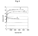
- FIG. 4 is a graph showing a relationship between efficiency and brightness of an organic light emitting display device according to ⁇ Exemplary embodiment 1>, ⁇ Exemplary embodiment 2>, and ⁇ Comparative example 1>.
- the organic light emitting display devices having multiple emission layers according to ⁇ Exemplary embodiment 1> (B) and ⁇ Exemplary embodiment 2> (C) are excellent in luminous efficiency compared to the organic light emitting display device having a single emission layer according to ⁇ Comparative example 1> (A). Further, even though the organic light emitting display device according to ⁇ Exemplary embodiment 1> (B) has better luminous efficiency than that of ⁇ Exemplary embodiment 2> (C), but a simple structure of ⁇ Exemplary embodiment 2> is more preferable in terms of the manufacturing process.
- the organic light emitting display device having the multiple emission layers needs a driving voltage increased by 3 through 4V, but the luminous efficiency increases as much as the stacked number of the emission layers.
- the present invention provides an organic light emitting display device having multiple emission layers, in which a small molecule organic material is interposed between emission layers to enhance interfacial properties between layers, thereby increasing luminous efficiency.
Landscapes
- Physics & Mathematics (AREA)
- Optics & Photonics (AREA)
- Chemical & Material Sciences (AREA)
- Engineering & Computer Science (AREA)
- Materials Engineering (AREA)
- Organic Chemistry (AREA)
- Electroluminescent Light Sources (AREA)
Abstract
Description
- The present invention relates to an organic light emitting display device, and more particularly, to an organic light emitting display device having multiple emission layers, in which a charge transport layer between the emission layers is formed of an organic material to thereby enhance interfacial properties between the layers.
- An organic light emitting display device has the advantages of being able to emit light by itself, being thin and lightweight, having an ideal structure including simple parts and formed by a simple process, ensuring high picture quality and a wide viewing angle, being able to near-perfectly reproduce a moving picture, and being capable of realizing high colour purity. Further, the organic light emitting display device has electrical properties of low power consumption and low driving voltage so that the organic light emitting display device is suitable for a mobile display.
- In general, the organic light emitting display device includes a substrate, a pixel electrode formed on the substrate, an organic layer comprising an emission layer (EML) formed on the pixel electrode, and a counter electrode formed on the organic layer. The organic layer may further include a hole injection layer (HIL) and a hole transport layer (HTL) between the pixel electrode and the emission layer (EML), and an electron transport layer (ETL) and an electron injection layer (EIL) between the emission layer (EML) and the counter electrode.
- The organic light emitting display device with this configuration operates as follows. When a voltage is applied between the pixel electrode and the counter electrode, a hole is injected from the pixel electrode to the emission layer via the hole injection layer (HIL) and the hole transport layer (HTL), and an electron is injected from the counter electrode to the emission layer via the electron injection layer (EIL) and the electron transport layer (ETL). Then, the hole and the electron are recombined in the emission layer, thereby creating an exciton. Thus, light is emitted while the exciton is transitioned from an excited state to a ground state.
- The organic light emitting display device includes an organic layer between the pixel electrode and the counter electrode to emit light, and is classified into a small molecule organic light emitting display device and a polymer organic light emitting display device according to the kind of the organic layer.
- A polymer has a structure in which tens through hundreds of monomer units (i.e., repeating units) are connected to one another by a covalent bond. Therefore, the polymer is more useful for forming a thin organic layer than small molecules, and a polymer organic layer has higher impact resistance than a small molecule organic layer. Further, the polymer includes not only a monomer for transporting holes but also a monomer for transporting electrons, so that early organic light emitting display devices were manufactured by interposing only the emission layer of the polymer between the pixel electrode and the counter electrode. In the meantime, there have been attempts to apply a multilayered structure to the polymer organic light emitting display device in order to optimise driving voltage, brightness and luminous efficiency.
- However, when a polymer emission layer is formed by a wet process such as a spin coating method or an ink jet method, a material for the hole injection layer (HIL) or the hole transport layer (HTL) which has been formed under the emission layer may be soluble in an organic solvent used in the wet process for forming the emission layer. Therefore, the material for the hole injection layer (HIL) or the hole transport layer (HTL) must not be soluble in the organic solvent. For example, water-soluble materials such as PEDOT (poly-3,4-ethylenedioxythiophene), PANI (polyaniline) or etc. are used for the hole transport layer (HTL). However, poor interfacial properties between the water-soluble hole transport layer (HTL) and the hydrophobic emission layer causes the device to be deteriorated, thereby decreasing the lifespan of the device.
-
Korean Patent Application No. 1997-0045389 - In an organic light emitting display device, a first electrode, a hole transport layer, a first emission layer, a charge transport layer, a second emission layer, an electron transport layer, an electron injection layer, and a second electrode are sequentially stacked on a substrate. Here, the first electrode and the second electrode may be used as a pixel electrode and a counter electrode, respectively. Further, the charge transport layer formed of inorganic material such as vanadium oxide (V2O5) serves to transport electrons to the first emission layer adjacent to the first electrode, and transport holes into the second emission layer adjacent to the second electrode. As the holes and the electrons are recombined in the respective emission layers, it is possible to increase luminous efficiency as much as the stacked number of the emission layers. However, the charge transport layer formed of an inorganic material such as vanadium oxide (V2O5) has an effect on a lower organic layer while being formed, so that processes are unstably performed. Further, a difference in layer-forming temperature between the organic layer and the inorganic layer deteriorates interfacial properties therebetween.
- The organic light emitting display device according to the present invention comprises a substrate; a first electrode formed on the substrate; a second electrode; at least two emission layers between the first electrode and the second electrode; and at least one organic charge transport layer between the emission layers.
- In other words, the present invention provides an organic light emitting display device having multiple emission layers, in which an organic charge transport layer is interposed between the emission layers to enhance interfacial properties between layers, thereby increasing luminous efficiency.
- The organic light emitting display device may further comprise at least one thin film transistor between the substrate and the first electrode.
- According to a preferred embodiment of the invention the charge transport layer has a HOMO ranging from 5.3 to 6.0eV and a LUMO ranging from 2.0 to 3.0eV. It further may have an electron mobility and a hole mobility which differ from each other by a factor of 100 or less.
- Further, the organic light emitting display device may further include at least one layer of a hole injection layer, a hole transport layer, a hole blocking layer, an electron transport layer and an electron injection layer, which is preferably formed of an organic material, particularly a small molecule organic material, fromed between the first electrode and the emission layer and/or between the second electrode and the emission layer. Each of these layers may be formed by a deposition method.
- According to an aspect of the present invention, an organic light emitting display includes: a substrate; a first electrode formed on the substrate; a first emission layer formed on the first electrode; a first charge transport layer formed on the first emission layer, the first charge transport layer comprising an organic material, the first charge transport layer capable of transporting electrons and holes; a second emission layer formed on the first charge transport layer; and a second electrode formed on the second emission layer. Herein the HOMO and the LUMO levels as well as the electron mobility and the hole mobility may have values as described above. The organic light emitting display device may further include at least one of a second charge transport layer between the first electrode and the first emission layer and a third charge transport layer between the second emission layer and the second electrode, the second and third charge transport layers comprising a small molecule organic material. Each of the first, second and third charge transport layers may be formed of N,N'-bis(1-naphthyl)-N,N'-dipheyl-1,1'biphenyl-4,4'diamine.
- According to an aspect of the present invention, an organic light emitting display device includes: a substrate; a first electrode formed on the substrate; a first emission layer formed on the first electrode; optionally at least one of a hole injection layer and a first hole transport layer between the first electrode and the first emission layer; a first electron transport layer formed on the first emission layer; a second hole transport layer formed on the first electron transport layer; a second emission layer formed on the second hole transport layer; a second electrode formed on the second emission layer; and optionally at least one of a hole blocking layer, a second electron transport layer and an electron injection layer between the second emission layer and the second electrode. In this structure the first electron transport layer may comprise Alq3 and the second hole transport layer may comprise CuPC and NPD. The first electron transport layer and the second electron transport layer are preferably formed of the same material. In the same way, the first hole transport layer and the second hole transport layer are preferably formed of the same material. Further, each of the first electron transport layer and the second hole transport layer may comprise a small molecule organic material.
- Further preferred embodiments of the present invention are subject matter of the depending claims.
- A more complete appreciation of the present invention, and many of the above and other features and advantages of the present invention, will be readily apparent as the same becomes better understood by reference to the following detailed description when considered in conjunction with the accompanying drawings in which like reference symbols indicate the same or similar components, wherein:
- FIG. 1 is a cross-sectional view of a general structure of an organic light emitting display device;
- FIG. 2 is a cross-sectional view of an organic light emitting display device according to an exemplary embodiment of the present invention;
- FIG. 3 is a cross-sectional view of an organic light emitting display device according to another exemplary embodiment of the present invention; and
- FIG. 4 is a graph showing a relationship between efficiency and brightness of the organic light emitting display device according to the present invention.
- The present invention will now be described more fully hereinafter with reference to the accompanying drawings, in which exemplary embodiments of the invention are shown.
- FIG. 1 is a general structure of an organic light emitting display device, in which a
first electrode 110, ahole transport layer 120, afirst emission layer 130, acharge transport layer 140, asecond emission layer 132, anelectron transport layer 150, anelectron injection layer 160, and asecond electrode 170 are sequentially stacked on asubstrate 100. Here, thefirst electrode 110 and thesecond electrode 170 may be used as a pixel electrode and a counter electrode, respectively. Further, thecharge transport layer 140 serves to transport electrons into thefirst emission layer 130 adjacent to thefirst electrode 110, and transport holes into thesecond emission layer 132 adjacent to thesecond electrode 170. As the holes and the electrons are recombined in the respective emission layers, it is possible to increase luminous efficiency as much as the stacked number of the emission layers. At this time, thefirst electrode 110 is formed of ITO (indium tin oxide). Thehole transport layer 120 has a stacked structure of CuPc (copper phthalocyanine) 122 and NPB (N,N'-bis(1-naphthyl)-N,N'-dipheyl-1,1'biphenyl-4,4'diamine) 124. The first andsecond emission layers electron transport layer 150 is formed of Alq3 (tris-(8-hydroxyquinoline)aluminum). Thecharge transport layer 140 is formed of vanadium oxide (V2O5). Theelectron injection layer 160 between theelectron transport layer 150 and thesecond electrode 170 is formed of lithium fluoride (LiF). Thecounter electrode 170 is formed of Al (aluminum). Preferably, a LiF layer is formed to have a thickness of about 10Å not only to enhance interfacial properties between an organic layer and a reflective electrode, but also to lower a work function of aluminum used as the reflective electrode. - When the charge transport layer is formed of an inorganic material such as vanadium oxide (V2O5), manufacturing processes are unstably performed because the inorganic layer has an effect on a lower organic layer while being formed. Further, a difference in layer-forming temperature between the organic layer and the inorganic layer deteriorates interfacial properties therebetween.
- FIG. 2 is a cross-sectional view of an organic light emitting display device according to an exemplary embodiment of the present invention.
- A
first electrode 210, afirst emission layer 230, acharge transport layer 240, asecond emission layer 232 and asecond electrode 270 are sequentially stacked on asubstrate 200. In the case where thefirst electrode 210 is used as a pixel electrode, one or more thin film transistors may be further disposed between thesubstrate 200 and thefirst electrode 210. At this time, the organic light emitting display device may have a top emission structure, a bottom emission structure, or a dual emission structure. - The
first electrode 210 is formed of a transparent electrode such as indium tin oxide, indium zinc oxide, etc. - The
charge transport layer 240 is formed of a small molecule organic material having a highest occupied molecular orbital (HOMO) level and a lowest unoccupied molecular orbital (LUMO) level, which are proper to transport an electron and a hole to the emission layer, and having a little difference between hole mobility and electron mobility. Thecharge transport layer 240 allows the electron or the hole to move to the first and second emission layers 230 and 232, thereby emitting light. Preferably, thecharge transport layer 240 has a HOMO level of 5.3 through 6.0eV, and a LUMO level of 2.0 through 3.0eV. Further, the electron mobility and the hole mobility of the charge transfer material are preferably different by a factor of no more than 100. The reason why the small molecule organic material is used for thecharge transport layer 240 is that it may be easily formed by a deposition method. In the case where thefirst electrode 210 is employed as the pixel electrode and thesecond electrode 270 is employed as a counter electrode, thecharge transport layer 240 transports the electrons and the holes to thefirst emission layer 230 and thesecond emission layer 232, respectively. - The
charge transport layer 240 may have a monolayer structure or a multilayer structure. For example, when thecharge transport layer 240 has a monolayer structure, it may include naphthyl-substituted benzidine derivative (NPB). On the other hand, when thecharge transport layer 240 has a multilayer structure, it may have a stacked structure of an electron transport layer and a hole transport layer, e.g., a stacked structure of Alq3, CuPC/NPB. - The
first emission layer 230 and thesecond emission layer 232 may be emission layers patterned corresponding to red, green and blue, and be formed of a phosphorescent material or a fluorescent material. Further, thefirst emission layer 230 and thesecond emission layer 232 may have the same colour or different colours. - When the
first emission layer 230 and thesecond emission layer 232 are red, a host material may include carbazole biphenyl (CBP) or 1,3-N,N-dicarbazole-benzene (mCP) and a dopant material may be a phosphorescent material including at least one selected from the group consisting of PIQIr ((acac)(bis(1-phenylisoquinoline)acetylacetonate iridium)), PQIr ((acac)(bis(1-phenylquinoline)acetylacetonate iridium)), PQIr (tris(1-phenylquinoline) iridium, and PtOEP (octaethylporphyrin platinum). Alternatively, the red emission layer may be formed of a fluorescent material such as 2-(4-biphenylyl)-5-phenyl-1,3,4-oxidiazole (PBD): tris(dibenzoylmethanido)(o-phenanthroline)europium(III) complex (Eu(DBM)3(Phen)) or perylene. - When the
first emission layer 230 and thesecond emission layer 232 are green, a host material may include CBP or mCP, and a dopant material may be a phosphorescent material including Ir(ppy)3 (fac tris(2-phenylpyridine) iridium). Further, the green emission layer may be formed of a fluorescent material such as Alq3(tris(8-hydroxylquinoline)aluminum). - When the
first emission layer 230 and thesecond emission layer 232 are blue, they may be formed of a fluorescent material because the optical properties of the blue emission layer are unstable when the blue emission layer is formed of a phosphorescent material. The fluorescent material may include one selected from the group consisting of 4,4-bis-(2,2-diphenyl-vinyl)-biphenyl (DPVBi), spiro-DPVBi, spiro-sexiphenyl (spiro-6P), DSB (distyrylbenzene), DSA (distyryl arylene), PFO (poly dioctyl-fluorene)-based polymer and PPV (polyphenylene vinylene)-based polymer. - The
first emission layer 230 and thesecond emission layer 232 may be formed in each unit pixel area by a laser induced thermal imaging method or a vacuum deposition method using a fine metal mask. - The
second electrode 270 may be formed of a metal material having a relatively low work function. For example, the metal material may include Al, MgAg, Ca, MgCa, etc. - FIG. 3 is a cross-sectional view of an organic light emitting display device according to another exemplary embodiment of the present invention.
- Referring to FIG. 3, a
first electrode 210; a hole transport and/orinjection layer 220; afirst emission layer 230; acharge transport layer 240; asecond emission layer 232; at least onelayer 255 of a hole blocking layer, an electron injection layer and an electron transport layer; asecond electrode 270 are sequentially stacked on asubstrate 200. In FIG. 3, the hole transport and/orinjection layer 220 is interposed between thefirst electrode 210 and thefirst emission layer 230, and the at least onelayer 255 of the hole blocking layer, the electron injection layer and the electron transport layer is interposed between thesecond electrode 270 and thesecond emission layer 232, but not limited thereto. Alternatively, either the hole transport and/orinjection layer 220 or the at least onelayer 255 of the hole blocking layer, the electron injection layer and the electron transport layer may be provided. - The hole transport and/or
injection layer 220 may have a monolayer of NPB or a stacked structure of CuPC/NPB. - The hole blocking layer, the electron transport layer and the electron injection layer are formed of a publicly known material. The hole injection layer, the hole transport layer, the hole blocking layer, the electron transport layer and the electron injection layer may be formed of a small molecule material, and one or more layers among them may be formed by a deposition method.
- Below, exemplary embodiments of the present invention will be described to facilitate understanding of the present invention, but the present invention is not limited to the following exemplary embodiments.
- ITO was patterned as a first electrode on a substrate, and a pixel area was defined. Then, NPB as a first charge transport layer was formed to a thickness of 600Å on the first electrode by a deposition method. Then, a stacked structure of Alq3 and C545T for a green emission layer was formed to a thickness of 300Å as the first emission layer on the first charge transport layer. NPB as a second charge transport layer was formed to a thickness of 300Å on the first emission layer. Then, a stacked structure of Alq3 and C545T, i.e.,10-(2-benzothiazolyl)-1,1,7,7-tetramethyl-2,3,6,7-tetrahydro-1H,5H,11H-[1]benzopyrano[6,7,8-ij]-quinolizin-11-one was formed to a thickness of 300Å as a second emission layer on the second charge transport layer. Then, NPB was formed to a thickness of 100Å as a third charge transport layer on the second emission layer. Then, a second electrode was formed of aluminum on the third charge transport layer. At this time, because the second electrode was formed of aluminum, LiF was formed to a thickness of 10Å in consideration of interfacial properties between the third charge transport layer and the second electrode.
- ITO was patterned as a first electrode on a substrate, and a pixel area was defined. Then, CuPC and NPB were formed to a thickness of 400Å and a thickness of 300Å, respectively, as a first hole transport layer on the first electrode. Then, a stacked structure of Alq3 and C545T for a green emission layer was formed to a thickness of 300Å as a first emission layer on the first hole transport layer. Then, Alq3 was formed to a thickness of 200Å as a first electron transport layer on the first emission layer. Then, CuPC and NPB were formed to a thickness of 300Å, respectively, as a second hole transport layer on the first electron transport layer. Then, a stacked structure of Alq3 and C545T was formed to a thickness of 300Å as a second emission layer on the second hole transport layer. Then, Alq3 was formed to a thickness of 200Å as a second electron transport layer on the second emission layer. Then, aluminum was formed as a second electrode on the second electron transport layer. At this time, because the second electrode was formed of aluminum, LiF was formed to a thickness of 10Å in consideration of interfacial properties between the second electron transport layer and the second electrode.
- A first electrode, a hole transport layer, an emission layer, a electron transport layer and a second electrode are sequentially stacked on the substrate, which are formed by the same method but different in the number of emission layers compared to < Exemplary embodiment 1>.
- FIG. 4 is a graph showing a relationship between efficiency and brightness of an organic light emitting display device according to <Exemplary embodiment 1>, <
Exemplary embodiment 2>, and <Comparative example 1>. - Referring to FIG. 4, the organic light emitting display devices having multiple emission layers according to <Exemplary embodiment 1> (B) and <
Exemplary embodiment 2> (C) are excellent in luminous efficiency compared to the organic light emitting display device having a single emission layer according to <Comparative example 1> (A). Further, even though the organic light emitting display device according to <Exemplary embodiment 1> (B) has better luminous efficiency than that of <Exemplary embodiment 2> (C), but a simple structure of <Exemplary embodiment 2> is more preferable in terms of the manufacturing process. - Thus, the organic light emitting display device having the multiple emission layers needs a driving voltage increased by 3 through 4V, but the luminous efficiency increases as much as the stacked number of the emission layers.
- As described above, the present invention provides an organic light emitting display device having multiple emission layers, in which a small molecule organic material is interposed between emission layers to enhance interfacial properties between layers, thereby increasing luminous efficiency.
- Although the present invention has been described with reference to certain exemplary embodiments thereof, it will be understood by those skilled in the art that a variety of modifications and variations may be made to the present invention without departing from the spirit or scope of the present invention defined in the appended claims, and their equivalents.
Claims (20)
- An organic light emitting display device, comprising:a substrate (200);a first electrode (210) formed on the substrate (200);a second electrode (270);at least two emission layers (230, 232) between the first electrode (210) and the second electrode (270); andat least one organic charge transport layer (240) between the emission layers (230, 232).
- The organic light emitting display device according to claim 1, further comprising at least one thin film transistor between the substrate (200) and the first electrode (210).
- The organic light emitting display device according to claim 1 or 2, wherein the charge transport layer (240) has a highest occupied molecular orbital level (HOMO) of 5.3 through 6.0eV and a lowest unoccupied molecular orbital level (LUMO) of 2.0 through 3.0eV.
- The organic light emitting display device according to one of the preceding clams, wherein the charge transport layer has electron mobility and hole mobility which are different by a factor of 100 or less.
- The organic light emitting display device according to one of the preceding clams, wherein the organic charge transport layer (240) is formed of N,N'-bis(1-naphthyl)-N,N'-dipheyl-1,1'biphenyl-4,4'diamine (NPD).
- The organic light emitting display device according to one of the preceding clams, wherein the organic charge transport layer (240) has a stacked structure of an electron transport layer and a hole transport layer.
- The organic light emitting display device according to claim 6, wherein the organic charge transport layer (240) has a stacked structure of tris-(8-hydroxyquinoline)aluminum (Alq3), copper phthalocyanine (CuPC) and N,N'-bis(1-naphthyl)-N,N'-dipheyl-1,1'biphenyl-4,4'diamine (NPD).
- The organic light emitting display device according to one of the preceding clams, wherein the organic charge transport layer (240) is formed of a small molecule organic material.
- The organic light emitting display device according to one of the preceding clams, wherein the organic charge transport layer (240) is formed by a deposition method.
- The organic light emitting display device according to one of the preceding clams, further comprising at least one layer (220) of a hole injection layer and a hole transport layer, and/or at least one layer (255) of a hole blocking layer, an electron transport layer and an electron injection layer, the at least one layer (220, 255) being disposed between the first electrode (210) and the second electrode (270).
- The organic light emitting display device according to claim 10, wherein the at least one layer (220) of the hole injection layer and the hole transport layer, and/or at least one layer (255) of the hole blocking layer, the electron transport layer and the electron injection layer is formed of a small molecule organic material.
- The organic light emitting display device according to claim 10 or 11, wherein the at least one layer (220) of the hole injection layer and the hole transport layer, and/or at least one layer (255) of the hole blocking layer, the electron transport layer and the electron injection layer is formed by a deposition method.
- The organic light emitting display device according to one of the clams 1 to 12, comprising:a substrate (200);a first electrode (210) formed on the substrate (200);a first emission layer (230) formed on the first electrode (210);a charge transport layer (240) formed on the first emission layer (230), the first charge transport layer (240) comprising an organic material, the first charge transport layer (240) capable of transporting electrons and holes;a second emission layer (232) formed on the first charge transport (240) layer; anda second electrode (270) formed on the second emission layer (232).
- The organic light emitting display device according to claim 13, wherein the first charge transport (240) layer has a highest occupied molecular orbital level (HOMO) of 5.3 through 6.0eV and a lowest unoccupied molecular orbital level (LUMO) of 2.0 through 3.0eV, and the first charge transport layer (240) has electron mobility and hole mobility which are different by a factor of 100 or less.
- The organic light emitting display device according to claim 13 or 14, further comprising:at least one of a second charge transport layer between the first electrode (210) and the first emission layer (230) and a third charge transport layer between the second emission layer (232) and the second electrode (270), the second and third charge transport layers comprising a small molecule organic material.
- The organic light emitting display device according to claim 15, wherein each of the first, second and third charge transport layers is formed of N,N'-bis(1-naphthyl)-N,N'-dipheyl-1,1'biphenyl-4,4'diamine.
- The organic light emitting display device according to one of the clams 1 to 12, comprising:a substrate;a first electrode formed on the substrate;a first emission layer formed on the first electrode;optionally at least one of a hole injection layer and a first hole transport layer between the first electrode and the first emission layer;a first electron transport layer formed on the first emission layer;a second hole transport layer formed on the first electron transport layer;a second emission layer formed on the second hole transport layer;a second electrode formed on the second emission layer; andoptionally at least one of a hole blocking layer, a second electron transport layer and an electron injection layer between the second emission layer and the second electrode.
- The organic light emitting display device according to claim 17, wherein the first electron transport layer comprises tris-(8-hydroxyquinoline)aluminum (Alq3), and the second hole transport layer comprises copper phthalocyanine (CuPC) and N,N'-bis(1-naphthyl)-N,N'-dipheyl-1,1'biphenyl-4,4'diamine (NPD).
- The organic light emitting display device according to claim 17 or 18, wherein the first electron transport layer and the second electron transport layer are formed of the same material, and the first hole transport layer and the second hole transport layer are formed of the same material.
- The organic light emitting display device according to one of claims 17 to 19, wherein each of the first electron transport layer and the second hole transport layer comprises a small molecule organic material.
Applications Claiming Priority (1)
| Application Number | Priority Date | Filing Date | Title |
|---|---|---|---|
| KR1020050063873A KR100712214B1 (en) | 2005-07-14 | 2005-07-14 | OLED display device |
Publications (2)
| Publication Number | Publication Date |
|---|---|
| EP1744382A1 true EP1744382A1 (en) | 2007-01-17 |
| EP1744382B1 EP1744382B1 (en) | 2013-06-19 |
Family
ID=37188936
Family Applications (1)
| Application Number | Title | Priority Date | Filing Date |
|---|---|---|---|
| EP06117192.2A Ceased EP1744382B1 (en) | 2005-07-14 | 2006-07-14 | Organic light emitting display device |
Country Status (3)
| Country | Link |
|---|---|
| US (1) | US20070013297A1 (en) |
| EP (1) | EP1744382B1 (en) |
| KR (1) | KR100712214B1 (en) |
Families Citing this family (11)
| Publication number | Priority date | Publication date | Assignee | Title |
|---|---|---|---|---|
| KR100774200B1 (en) * | 2006-04-13 | 2007-11-08 | 엘지전자 주식회사 | Organic EL element and its manufacturing method |
| DE102007058005B4 (en) * | 2007-09-25 | 2018-05-17 | Osram Oled Gmbh | Radiation-emitting device and method for its production |
| KR20090092051A (en) * | 2008-02-26 | 2009-08-31 | 삼성모바일디스플레이주식회사 | Organic light emitting diode and fabrication method for the same |
| TWI491087B (en) * | 2009-08-26 | 2015-07-01 | Univ Nat Taiwan | Suspension or solution of transition metal oxide for organic photoelectric element, preparation method and application thereof |
| TWI506121B (en) * | 2010-03-31 | 2015-11-01 | Semiconductor Energy Lab | Light-emitting element, light-emitting device, electronic device, and lighting device |
| DE102010041331A1 (en) * | 2010-09-24 | 2012-03-29 | Siemens Aktiengesellschaft | Charge carrier modulation for color and brightness tuning in organic light-emitting diodes |
| JP2015049972A (en) * | 2013-08-30 | 2015-03-16 | 株式会社ジャパンディスプレイ | Organic el display device |
| KR20150040118A (en) * | 2013-10-04 | 2015-04-14 | 엘지디스플레이 주식회사 | Organic emitting device and organic emitting display device comprising the same |
| KR102126544B1 (en) * | 2013-12-30 | 2020-06-24 | 엘지디스플레이 주식회사 | Organic electroluminescent device and organic electroluminescent display |
| CN106024844B (en) * | 2016-07-27 | 2019-01-22 | 京东方科技集团股份有限公司 | Organic light-emitting device, preparation method thereof, and display device |
| KR102583620B1 (en) * | 2018-11-23 | 2023-09-26 | 엘지디스플레이 주식회사 | Light emitting diode and light emitting device having the diode |
Citations (4)
| Publication number | Priority date | Publication date | Assignee | Title |
|---|---|---|---|---|
| US20020027416A1 (en) * | 2000-03-27 | 2002-03-07 | Dong-Hyun Kim | Organic electroluminescent device including charge transport buffer layer |
| EP1318553A2 (en) * | 2001-12-05 | 2003-06-11 | Sel Semiconductor Energy Laboratory Co., Ltd. | Organic semicondutor element |
| EP1478025A2 (en) | 2003-05-13 | 2004-11-17 | EASTMAN KODAK COMPANY (a New Jersey corporation) | Cascaded organic electroluminescent device having connecting units with n-type and p-type organic layers |
| US20050077817A1 (en) * | 2002-12-26 | 2005-04-14 | Semiconductor Energy Laboratory Co., Ltd. | Organic light emitting element and a light emitting device using the same |
Family Cites Families (7)
| Publication number | Priority date | Publication date | Assignee | Title |
|---|---|---|---|---|
| KR100435203B1 (en) * | 2001-08-17 | 2004-06-09 | 주식회사 진우엔지니어링 | White light-emitting organic electroluminescent device for back light and liquid crystal display device using itself |
| JP4216008B2 (en) * | 2002-06-27 | 2009-01-28 | 株式会社半導体エネルギー研究所 | LIGHT EMITTING DEVICE AND ITS MANUFACTURING METHOD, AND VIDEO CAMERA, DIGITAL CAMERA, GOGGLE TYPE DISPLAY, CAR NAVIGATION, PERSONAL COMPUTER, DVD PLAYER, ELECTRONIC GAME EQUIPMENT, OR PORTABLE INFORMATION TERMINAL HAVING THE LIGHT EMITTING DEVICE |
| US6811896B2 (en) * | 2002-07-29 | 2004-11-02 | Xerox Corporation | Organic light emitting device (OLED) with thick (100 to 250 nanometers) porphyrin buffer layer |
| KR100490118B1 (en) * | 2003-04-01 | 2005-05-17 | 한국전자통신연구원 | Organic light-emitting device |
| KR100544138B1 (en) * | 2003-11-12 | 2006-01-23 | 삼성에스디아이 주식회사 | Active Matrix Organic Light Emitting Diode |
| JP4393249B2 (en) * | 2004-03-31 | 2010-01-06 | 株式会社 日立ディスプレイズ | ORGANIC LIGHT EMITTING ELEMENT, IMAGE DISPLAY DEVICE, AND MANUFACTURING METHOD THEREOF |
| US20060214564A1 (en) * | 2005-03-24 | 2006-09-28 | Hsi-Ming Chang | Organic electroluminescent display and method for fabricating the same |
-
2005
- 2005-07-14 KR KR1020050063873A patent/KR100712214B1/en not_active Expired - Fee Related
-
2006
- 2006-07-14 EP EP06117192.2A patent/EP1744382B1/en not_active Ceased
- 2006-07-14 US US11/485,956 patent/US20070013297A1/en not_active Abandoned
Patent Citations (4)
| Publication number | Priority date | Publication date | Assignee | Title |
|---|---|---|---|---|
| US20020027416A1 (en) * | 2000-03-27 | 2002-03-07 | Dong-Hyun Kim | Organic electroluminescent device including charge transport buffer layer |
| EP1318553A2 (en) * | 2001-12-05 | 2003-06-11 | Sel Semiconductor Energy Laboratory Co., Ltd. | Organic semicondutor element |
| US20050077817A1 (en) * | 2002-12-26 | 2005-04-14 | Semiconductor Energy Laboratory Co., Ltd. | Organic light emitting element and a light emitting device using the same |
| EP1478025A2 (en) | 2003-05-13 | 2004-11-17 | EASTMAN KODAK COMPANY (a New Jersey corporation) | Cascaded organic electroluminescent device having connecting units with n-type and p-type organic layers |
Also Published As
| Publication number | Publication date |
|---|---|
| KR100712214B1 (en) | 2007-04-27 |
| EP1744382B1 (en) | 2013-06-19 |
| US20070013297A1 (en) | 2007-01-18 |
| KR20070008973A (en) | 2007-01-18 |
Similar Documents
| Publication | Publication Date | Title |
|---|---|---|
| US6875320B2 (en) | Highly transparent top electrode for OLED device | |
| KR101407574B1 (en) | White light emitting device | |
| KR101234469B1 (en) | Intermediate electrodes for stacked OLEDs | |
| EP1801882B1 (en) | Organic luminescence display device and method of manufacturing the same | |
| US9655199B2 (en) | Four component phosphorescent OLED for cool white lighting application | |
| US6905788B2 (en) | Stabilized OLED device | |
| CN100502086C (en) | Cascaded organic electroluminescent devices with connected units of N-type and P-type organic layers | |
| CN100483728C (en) | Organic electroluminescent device of electroluminescent unit with lamina | |
| US20080122348A1 (en) | Organic light emitting display device and method of fabricating the same | |
| US20090045739A1 (en) | Organic light emitting diode display device and method of fabricating the same | |
| US20090091255A1 (en) | White organic light emitting device | |
| US20050112403A1 (en) | Full color organic electroluminescent device | |
| JP2006156390A (en) | Organic electroluminescent device and manufacturing method thereof | |
| KR20100129279A (en) | Tandem ΟLED device with intermediate connector | |
| US20070182316A1 (en) | OLED with Area Defined Multicolor Emission Within a Single Lighting Element | |
| KR20060020029A (en) | A method of manufacturing an organic electroluminescent device manufactured using a donor substrate for laser transfer and a film thereof | |
| US20070241675A1 (en) | Organic electroluminescence device with charge separation layer | |
| EP1402758A1 (en) | Three-terminal organic electro-luminescent device | |
| EP1744382B1 (en) | Organic light emitting display device | |
| KR101434359B1 (en) | White Organic light emitting device | |
| US20050136289A1 (en) | White organic light emitting device | |
| US20050208332A1 (en) | White-light-emitting organic electroluminescent device and organic electroluminescent display having the same | |
| US7304428B2 (en) | Multilayered cathode structures having silver for OLED devices | |
| KR100924144B1 (en) | Organic electroluminescent device and manufacturing method thereof | |
| KR100594775B1 (en) | White organic light emitting device |
Legal Events
| Date | Code | Title | Description |
|---|---|---|---|
| PUAI | Public reference made under article 153(3) epc to a published international application that has entered the european phase |
Free format text: ORIGINAL CODE: 0009012 |
|
| 17P | Request for examination filed |
Effective date: 20060714 |
|
| AK | Designated contracting states |
Kind code of ref document: A1 Designated state(s): AT BE BG CH CY CZ DE DK EE ES FI FR GB GR HU IE IS IT LI LT LU LV MC NL PL PT RO SE SI SK TR |
|
| AX | Request for extension of the european patent |
Extension state: AL BA HR MK YU |
|
| AKX | Designation fees paid |
Designated state(s): DE FR GB |
|
| 17Q | First examination report despatched |
Effective date: 20070829 |
|
| RAP1 | Party data changed (applicant data changed or rights of an application transferred) |
Owner name: SAMSUNG MOBILE DISPLAY CO., LTD. |
|
| RAP1 | Party data changed (applicant data changed or rights of an application transferred) |
Owner name: SAMSUNG DISPLAY CO., LTD. |
|
| REG | Reference to a national code |
Ref country code: DE Ref legal event code: R079 Ref document number: 602006036848 Country of ref document: DE Free format text: PREVIOUS MAIN CLASS: H01L0051520000 Ipc: H01L0051500000 |
|
| GRAP | Despatch of communication of intention to grant a patent |
Free format text: ORIGINAL CODE: EPIDOSNIGR1 |
|
| RIC1 | Information provided on ipc code assigned before grant |
Ipc: H01L 51/52 20060101ALI20130124BHEP Ipc: H01L 51/50 20060101AFI20130124BHEP |
|
| GRAS | Grant fee paid |
Free format text: ORIGINAL CODE: EPIDOSNIGR3 |
|
| GRAA | (expected) grant |
Free format text: ORIGINAL CODE: 0009210 |
|
| AK | Designated contracting states |
Kind code of ref document: B1 Designated state(s): DE FR GB |
|
| REG | Reference to a national code |
Ref country code: GB Ref legal event code: FG4D |
|
| REG | Reference to a national code |
Ref country code: DE Ref legal event code: R096 Ref document number: 602006036848 Country of ref document: DE Effective date: 20130814 |
|
| PLBE | No opposition filed within time limit |
Free format text: ORIGINAL CODE: 0009261 |
|
| STAA | Information on the status of an ep patent application or granted ep patent |
Free format text: STATUS: NO OPPOSITION FILED WITHIN TIME LIMIT |
|
| 26N | No opposition filed |
Effective date: 20140320 |
|
| REG | Reference to a national code |
Ref country code: DE Ref legal event code: R097 Ref document number: 602006036848 Country of ref document: DE Effective date: 20140320 |
|
| REG | Reference to a national code |
Ref country code: FR Ref legal event code: PLFP Year of fee payment: 11 |
|
| REG | Reference to a national code |
Ref country code: FR Ref legal event code: PLFP Year of fee payment: 12 |
|
| REG | Reference to a national code |
Ref country code: FR Ref legal event code: PLFP Year of fee payment: 13 |
|
| REG | Reference to a national code |
Ref country code: DE Ref legal event code: R079 Ref document number: 602006036848 Country of ref document: DE Free format text: PREVIOUS MAIN CLASS: H01L0051500000 Ipc: H10K0050000000 |
|
| P01 | Opt-out of the competence of the unified patent court (upc) registered |
Effective date: 20230515 |
|
| PGFP | Annual fee paid to national office [announced via postgrant information from national office to epo] |
Ref country code: GB Payment date: 20240620 Year of fee payment: 19 |
|
| PGFP | Annual fee paid to national office [announced via postgrant information from national office to epo] |
Ref country code: FR Payment date: 20240624 Year of fee payment: 19 |
|
| PGFP | Annual fee paid to national office [announced via postgrant information from national office to epo] |
Ref country code: DE Payment date: 20240620 Year of fee payment: 19 |
|
| REG | Reference to a national code |
Ref country code: DE Ref legal event code: R119 Ref document number: 602006036848 Country of ref document: DE |
|
| GBPC | Gb: european patent ceased through non-payment of renewal fee |
Effective date: 20250714 |
|
| PG25 | Lapsed in a contracting state [announced via postgrant information from national office to epo] |
Ref country code: GB Free format text: LAPSE BECAUSE OF NON-PAYMENT OF DUE FEES Effective date: 20250714 |
|
| PG25 | Lapsed in a contracting state [announced via postgrant information from national office to epo] |
Ref country code: DE Free format text: LAPSE BECAUSE OF NON-PAYMENT OF DUE FEES Effective date: 20260203 |
|
| PG25 | Lapsed in a contracting state [announced via postgrant information from national office to epo] |
Ref country code: FR Free format text: LAPSE BECAUSE OF NON-PAYMENT OF DUE FEES Effective date: 20250731 |