EP1744352A2 - Method for forming a fully germano-silicided gate mosfet and devices obtained thereof - Google Patents
Method for forming a fully germano-silicided gate mosfet and devices obtained thereof Download PDFInfo
- Publication number
- EP1744352A2 EP1744352A2 EP06447038A EP06447038A EP1744352A2 EP 1744352 A2 EP1744352 A2 EP 1744352A2 EP 06447038 A EP06447038 A EP 06447038A EP 06447038 A EP06447038 A EP 06447038A EP 1744352 A2 EP1744352 A2 EP 1744352A2
- Authority
- EP
- European Patent Office
- Prior art keywords
- nickel
- gate electrode
- sige
- germano
- layer
- Prior art date
- Legal status (The legal status is an assumption and is not a legal conclusion. Google has not performed a legal analysis and makes no representation as to the accuracy of the status listed.)
- Withdrawn
Links
Images




Classifications
-
- H—ELECTRICITY
- H10—SEMICONDUCTOR DEVICES; ELECTRIC SOLID-STATE DEVICES NOT OTHERWISE PROVIDED FOR
- H10D—INORGANIC ELECTRIC SEMICONDUCTOR DEVICES
- H10D64/00—Electrodes of devices having potential barriers
- H10D64/01—Manufacture or treatment
- H10D64/017—Manufacture or treatment using dummy gates in processes wherein at least parts of the final gates are self-aligned to the dummy gates, i.e. replacement gate processes
-
- H—ELECTRICITY
- H10—SEMICONDUCTOR DEVICES; ELECTRIC SOLID-STATE DEVICES NOT OTHERWISE PROVIDED FOR
- H10D—INORGANIC ELECTRIC SEMICONDUCTOR DEVICES
- H10D64/00—Electrodes of devices having potential barriers
- H10D64/01—Manufacture or treatment
- H10D64/013—Manufacture or treatment of electrodes having a conductor capacitively coupled to a semiconductor by an insulator
- H10D64/01302—Manufacture or treatment of electrodes having a conductor capacitively coupled to a semiconductor by an insulator the insulator being formed after the semiconductor body, the semiconductor being silicon
- H10D64/01304—Manufacture or treatment of electrodes having a conductor capacitively coupled to a semiconductor by an insulator the insulator being formed after the semiconductor body, the semiconductor being silicon characterised by the conductor
- H10D64/01318—Manufacture or treatment of electrodes having a conductor capacitively coupled to a semiconductor by an insulator the insulator being formed after the semiconductor body, the semiconductor being silicon characterised by the conductor the conductor comprising a layer of alloy material, compound material or organic material contacting the insulator, e.g. TiN
- H10D64/0132—Manufacture or treatment of electrodes having a conductor capacitively coupled to a semiconductor by an insulator the insulator being formed after the semiconductor body, the semiconductor being silicon characterised by the conductor the conductor comprising a layer of alloy material, compound material or organic material contacting the insulator, e.g. TiN the conductor being a metallic silicide
-
- H—ELECTRICITY
- H10—SEMICONDUCTOR DEVICES; ELECTRIC SOLID-STATE DEVICES NOT OTHERWISE PROVIDED FOR
- H10D—INORGANIC ELECTRIC SEMICONDUCTOR DEVICES
- H10D64/00—Electrodes of devices having potential barriers
- H10D64/60—Electrodes characterised by their materials
- H10D64/66—Electrodes having a conductor capacitively coupled to a semiconductor by an insulator, e.g. MIS electrodes
- H10D64/667—Electrodes having a conductor capacitively coupled to a semiconductor by an insulator, e.g. MIS electrodes the conductor comprising a layer of alloy material, compound material or organic material contacting the insulator, e.g. TiN workfunction layers
- H10D64/668—Electrodes having a conductor capacitively coupled to a semiconductor by an insulator, e.g. MIS electrodes the conductor comprising a layer of alloy material, compound material or organic material contacting the insulator, e.g. TiN workfunction layers the layer being a silicide, e.g. TiSi2
-
- H—ELECTRICITY
- H10—SEMICONDUCTOR DEVICES; ELECTRIC SOLID-STATE DEVICES NOT OTHERWISE PROVIDED FOR
- H10D—INORGANIC ELECTRIC SEMICONDUCTOR DEVICES
- H10D64/00—Electrodes of devices having potential barriers
- H10D64/60—Electrodes characterised by their materials
- H10D64/66—Electrodes having a conductor capacitively coupled to a semiconductor by an insulator, e.g. MIS electrodes
- H10D64/68—Electrodes having a conductor capacitively coupled to a semiconductor by an insulator, e.g. MIS electrodes characterised by the insulator, e.g. by the gate insulator
- H10D64/691—Electrodes having a conductor capacitively coupled to a semiconductor by an insulator, e.g. MIS electrodes characterised by the insulator, e.g. by the gate insulator comprising metallic compounds, e.g. metal oxides or metal silicates
-
- H—ELECTRICITY
- H10—SEMICONDUCTOR DEVICES; ELECTRIC SOLID-STATE DEVICES NOT OTHERWISE PROVIDED FOR
- H10D—INORGANIC ELECTRIC SEMICONDUCTOR DEVICES
- H10D30/00—Field-effect transistors [FET]
- H10D30/60—Insulated-gate field-effect transistors [IGFET]
- H10D30/62—Fin field-effect transistors [FinFET]
-
- H—ELECTRICITY
- H10—SEMICONDUCTOR DEVICES; ELECTRIC SOLID-STATE DEVICES NOT OTHERWISE PROVIDED FOR
- H10D—INORGANIC ELECTRIC SEMICONDUCTOR DEVICES
- H10D84/00—Integrated devices formed in or on semiconductor substrates that comprise only semiconducting layers, e.g. on Si wafers or on GaAs-on-Si wafers
- H10D84/01—Manufacture or treatment
- H10D84/0123—Integrating together multiple components covered by H10D12/00 or H10D30/00, e.g. integrating multiple IGBTs
- H10D84/0126—Integrating together multiple components covered by H10D12/00 or H10D30/00, e.g. integrating multiple IGBTs the components including insulated gates, e.g. IGFETs
- H10D84/0165—Integrating together multiple components covered by H10D12/00 or H10D30/00, e.g. integrating multiple IGBTs the components including insulated gates, e.g. IGFETs the components including complementary IGFETs, e.g. CMOS devices
- H10D84/0172—Manufacturing their gate conductors
- H10D84/0174—Manufacturing their gate conductors the gate conductors being silicided
-
- H—ELECTRICITY
- H10—SEMICONDUCTOR DEVICES; ELECTRIC SOLID-STATE DEVICES NOT OTHERWISE PROVIDED FOR
- H10D—INORGANIC ELECTRIC SEMICONDUCTOR DEVICES
- H10D84/00—Integrated devices formed in or on semiconductor substrates that comprise only semiconducting layers, e.g. on Si wafers or on GaAs-on-Si wafers
- H10D84/01—Manufacture or treatment
- H10D84/0123—Integrating together multiple components covered by H10D12/00 or H10D30/00, e.g. integrating multiple IGBTs
- H10D84/0126—Integrating together multiple components covered by H10D12/00 or H10D30/00, e.g. integrating multiple IGBTs the components including insulated gates, e.g. IGFETs
- H10D84/0165—Integrating together multiple components covered by H10D12/00 or H10D30/00, e.g. integrating multiple IGBTs the components including insulated gates, e.g. IGFETs the components including complementary IGFETs, e.g. CMOS devices
- H10D84/0172—Manufacturing their gate conductors
- H10D84/0177—Manufacturing their gate conductors the gate conductors having different materials or different implants
-
- H—ELECTRICITY
- H10—SEMICONDUCTOR DEVICES; ELECTRIC SOLID-STATE DEVICES NOT OTHERWISE PROVIDED FOR
- H10D—INORGANIC ELECTRIC SEMICONDUCTOR DEVICES
- H10D84/00—Integrated devices formed in or on semiconductor substrates that comprise only semiconducting layers, e.g. on Si wafers or on GaAs-on-Si wafers
- H10D84/01—Manufacture or treatment
- H10D84/02—Manufacture or treatment characterised by using material-based technologies
- H10D84/03—Manufacture or treatment characterised by using material-based technologies using Group IV technology, e.g. silicon technology or silicon-carbide [SiC] technology
- H10D84/038—Manufacture or treatment characterised by using material-based technologies using Group IV technology, e.g. silicon technology or silicon-carbide [SiC] technology using silicon technology, e.g. SiGe
Definitions
- the present invention relates to semiconductor process technology and devices.
- the present invention relates to semiconductor devices with metallic gate electrodes formed by a reaction between a metal and a semiconductor material.
- CMOS Complementary-Metal-Oxide-Silicon
- MOSFET Metal-Oxide-Silicon Field Effect Transistors
- the scaling of the MOSFET causes manufacturers of electronic devices to replace well-known and widely used materials, such as silicon and silicon-oxide, with novel materials. These novel materials need to be compatible with and easily implemented in a mainstream MOS process flow. Dielectric materials having a dielectric constant larger than silicon-oxide are introduced to form gate dielectric.
- metal oxides such as HfSiO 2 , HfSi, and Al 2 O 3
- metal oxides are selected as a high-k dielectric.
- COT Capacitive Oxide Thickness
- high-k dielectrics allow forming a physically thicker layer in comparison with a silicon-oxide.
- metals are considered as replacements for polycrystalline silicon.
- Metal gate electrodes can be formed by full silicidation (FUSI) of the polysilicon gate electrode with a metal, such as nickel, cobalt, tungsten, and so on. During this silicidation process the complete polysilicon gate electrode is converted into a silicide.
- the metal must have the appropriate work function in order to obtain the desired low threshold voltage.
- the work function should be in the range 4 to 4.2eV if the metal is used to form the gate electrode of an nMOSFET and in the range 5 to 5.2eV when used to form the gate electrode of a pMOSFET.
- fully silicided gate electrodes are formed by NiSi, although NiSi has a near-midgap work function resulting in a large threshold voltage for nMOSFET and pMOSFET.
- the selected high-k dielectric and metal should not influence the work function of the gate electrode.
- defects and charges within the gate stack can result in a threshold voltage shift.
- the interaction between the gate electrode and the gate dielectric will, at their interface, fix the Fermi level to an unwanted value. This phenomenon of Fermi level pinning is known to cause a high threshold voltage for metal gates.
- WO2004/038807 describes a method for forming a MOSFET transistor comprising a gate electrode comprising a nickel germano-silicide layer, resulting from the silicidation of a silicon germanium layer with a composition Si 1-x Ge x where x is typically comprised between 0,1 and 0,3.
- the work function of the metal must be adjustable so that the metal can be used as a gate electrode material for pMOSFET devices requiring a low threshold voltage.
- This metal should be easy introducible in a mainstream MOS or CMOS process flow.
- a gate electrode material that doesn't suffer from Fermi level pinning at the interface between the metal and the high-k dielectric, in particular when the gate dielectric comprises hafnium.
- y can be comprised between 0,5 and 0,8, or preferably between 0,55 and 0,8.
- x can be equal to 0,5 and y equal to 0,5, or preferably x is equal to 0,45 and y equal to 0,55, and even more preferably x is equal to 0,35 and y equal to 0,65.
- the gate dielectric comprises hafnium and silicon, and more particularly, the gate dielectric is an HfSiON dielectric.
- the invention also relates to said process.
- a metallic alloy according to the invention can be used as a high work function (i.e. higher than 4,5eV) material.
- the invention also relates to a method for forming a pMOSFET, comprising:
- y is comprised between about 0,5 and about 0,8, preferably 0,5 ⁇ y ⁇ 0,8 or more preferably 0,5 ⁇ y ⁇ 0,8.
- said gate electrode (4) is (uniformly) deposited by means of a Chemical Vapor Deposition (CVD) process.
- CVD Chemical Vapor Deposition
- SiH 4 and GeH 4 can be used as precursors in said CVD process.
- a method according to the invention can further comprise the step of selectively removing the unreacted metal after forming the metal germano-silicided gate electrode.
- said nickel is provided in a sufficient amount for obtaining a nickel germano-silicide wherein the ratio nickel-to-SiGe is larger than 1, such as Ni 2 (SiGe), Ni 3 (SiGe) 2 , Ni 31 (SiGe) 12 , or Ni 3 (SiGe).
- a method according to the invention can further comprise the steps of forming a dielectric layer over said silicon-germanium layer, the source and drain junction regions and then the step of exposing the said silicon-germanium layer before depositing said metal layer stack.
- a method of the invention for reducing the threshold voltage of a pMOSFET device preferably further comprises the step of providing nickel in a sufficient amount for obtaining a nickel germano-silicide wherein the ratio nickel-to-SiGe is larger than 1, such as Ni 2 (SiGe), Ni 3 (SiGe) 2 , Ni 31 (SiGe) 12 , or Ni 3 (SiGe).
- the threshold voltage of the MOSFET can be controlled by controlling the germanium content of the Si x Ge y layer.
- the threshold voltage of the MOSFET can further be controlled by controlling the nickel content provided for the annealing step.
- the gate dielectric of this MOSFET comprises hafnium and silicon.
- this gate dielectric is an HfSiON dielectric.
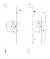
- Figures 1a-d show schematic cross-sections illustrating various steps of a process flow, according to an example.
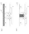
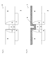
- Figures 2a-e show schematic cross-sections illustrating various steps of a process flow, according to an example.
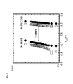
- Figure 3 is a graph that shows the threshold voltage distribution for different gate dielectrics of a fully nickel silicided MOS devices (FUSI) and fully nickel germano-silicided MOS devices (FUSIGE), according to an example.
- FUSI fully nickel silicided MOS devices
- FUSIGE fully nickel germano-silicided MOS devices
- Figure 4 is a graph that shows the threshold voltage of a fully nickel silicided MOS device (FUSI) and fully nickel germano-silicided MOS devices (FUSIGE), according to an example with varying germanium content.
- FUSI fully nickel silicided MOS device
- FUSIGE fully nickel germano-silicided MOS devices
- Figure 5 is a graph that shows the workfunction of a fully nickel germano-silicided MOS device (FUSIGE) according to an example with varying nickel content.
- FUSIGE fully nickel germano-silicided MOS device
- the gate dielectric of this MOSFET comprises hafnium and silicon.
- this gate dielectric is an HfSiON dielectric.
- the MOSFET can be formed by providing a transistor (a MOSFET) having a semiconductor gate electrode comprising silicon and germanium; forming, at least on part of the semiconductor gate electrode, a metal layer stack comprising Nickel; and transforming the semiconductor gate electrode into a Nickel Germanium Silicon gate electrode.
- a MOSFET transistor having a semiconductor gate electrode comprising silicon and germanium
- a metal layer stack comprising Nickel
- This fully germano-silicided gate electrode is a high work function metallic alloy.
- the method can further comprise selectively removing unreacted metal after silicidation of the silicon-germanium.
- the method can further comprise forming a dielectric layer over the semiconductor gate electrode and exposing the semiconductor gate electrode before depositing the metal layer stack.
- the gate dielectric comprises hafnium and silicon, and more particularly, the gate dielectric is an HfSiON dielectric.
- a method for manufacturing said MOSFET can comprise the steps of:
- the work function of the fully germano-silicided gate electrode can be tuned by varying the Ge content of the semiconductor material.
- a method of the invention can be used for reducing the threshold voltage of a pMOSFET.
- said threshold voltage can be further reduced.
- metal-rich phases such as Ni 3 (SiGe)2, Ni 2 (SiGe), Ni 31 (SiGe) 12 , and Ni 3 (SiGe) are particularly suitable as FUSI gate electrode material for pMOS transistors.
- nickel-rich-germano-silicide or “nickel-rich-germano-silicided phase” refers to the material resulting from the reaction between said nickel and said semiconductor, wherein the ratio nickel-to-semiconductor (i.e. Ni-to-SiGe) is larger than 1.
- FIGS. 1a-d schematically illustrate a process flow.
- Figure 1a shows a MOSFET device (1) formed on a substrate (2) comprising a gate electrode (4), a gate dielectric (3) in-between the gate electrode (4) and the substrate (2), sidewall spacers (5) formed in a dielectric material adjacent the stack of gate electrode (4) and gate dielectric (3), source (6) and drain (7) junction regions aligned to the gate stack (4, 3) and extending underneath the sidewall spacers (5).
- the transistor (1) shown in Figure 1a can be any type of Metal-Oxide-Semiconductor Field-Effect-Transistor (MOSFET), such as a bulk transistor, a Multiple Gate transistor (MuGFET), such as a FinFET device.
- MOSFET Metal-Oxide-Semiconductor Field-Effect-Transistor
- a bulk transistor such as a bulk transistor
- MuGFET Multiple Gate transistor
- FinFET device such as a FinFET device.
- the transistor (1) is a pMOSFET.
- the gate dielectric (3) can be a siliconoxide, a siliconoxynitride, a high-k dielectric comprising hafnium, such as hafniumoxides hafniumoxyntrides, hafniumsilicates.
- the gate dielectric (3) is a hafniumsiliconoxynitride (also referred to as Hf x Si y ON) such as HfSiON.
- the gate electrode is formed from Si 0.5 Ge 0.5 .
- said gate electrode (4) can be (uniformly) deposited by means of a Chemical Vapor Deposition (CVD) process.
- CVD Chemical Vapor Deposition
- the substrate (2) can be a bulk semiconductor substrate, such as a silicon or germanium wafer, a semiconductor-on-insulator substrate, such as Silicon-On-Insulator (SOI) and Germanium-In-Insulator (GeOI).
- a bulk semiconductor substrate such as a silicon or germanium wafer
- a semiconductor-on-insulator substrate such as Silicon-On-Insulator (SOI) and Germanium-In-Insulator (GeOI).
- the sidewall spacers (5) alongside the gate stack of gate electrode (4) and gate dielectric (3) are formed by depositing a conformal layer or stack of layers of dielectric material over the gate stack and by anisotropic etching of this dielectric layer(s) until the gate electrode (4) is exposed as is known in the art.
- silicon-oxide, siliconoxynitride, silicon-nitride, or silicon-carbide materials are conformally deposited and etched using a dry etch, such as a reactive ion etch (RIE) or etch plasma.
- RIE reactive ion etch
- the source (6) and drain (7) regions can be silicided using a self-aligned silicidation process.
- Standard semiconductor processes as known and appreciated by any person skilled in the art can be carried out for forming said gate dielectric (3), said sidewall pacers (5) and said source (6) and drain (7) regions.
- a dielectric layer stack (8) is deposited over the MOSFET device.
- This layer can be a silicon-oxide layer deposited by Chemical Vapor Deposition (CVD).
- This dielectric layer stack (8) is planarized by Chemical Mechanical Polishing (CMP) until the gate electrode (4) is exposed.
- CMP Chemical Mechanical Polishing
- This dielectric layer stack (8) shields the source (6) and drain (7) regions when forming the fully silicided gate electrode (10).
- this process step is optional and can be postponed until the fully silicided gate (10) is formed.
- optional silicidation of the gate electrode (4) can be done together with the silicidation of the source (6) and drain (7) regions.
- a layer (9) of silicidation metal(s) is deposited overlying at least the gate electrode (4).
- This layer of silicidation metal(s) comprises nickel.
- the layer (9) of silicidation metal(s) is a layer of nickel.
- the semiconductor material(s) of the gate electrode (4) and the silicidation metal(s) (9) have reacted in a self-aligned process to form a fully silicided gate electrode (10).
- a fully silicided gate electrode (10) Sufficient thermal energy is provided to have the electrode comprising Si and Ge react with the silicidation metal comprising nickel and to form a fully germano-silicided gate electrode.
- Si 0.5 Ge 0.5 is used to form the gate electrode (4) and nickel is used as silicidation metal (9) and a nickel-silicon-germanium Ni 3 (SiGe) 2 (10) is formed.
- a fully germano-silicided pMOSFET is formed as illustrated by Figures 2a-e.
- Hf x Si y ON layers are uniformly deposited using a Metal Organic Chemical Vapor Deposition (MOCVD) on an n-type substrate (2) to form the gate dielectric (3).
- MOCVD Metal Organic Chemical Vapor Deposition
- the thickness and the composition of this dielectric layer is varied from one substrate to another: about 2 nm HfSiON with Hf/Si ratio of about 23/77, about 3 nm HfSiON with Hf/Si ratio of about 53/47 and about 3 nm HfSiON with Hf/Si ratio of about 65/35.
- a layer of about 100 nm undoped Si 0.5 Ge 0.5 is uniformly deposited over a dielectric layer on a substrate (2) using SiH 4 and GeH 4 as precursor in a Chemical Vapor Deposition (CVD) process to form the gate electrode (4).
- CVD Chemical Vapor Deposition
- An oxide layer (11) of about 60 nm is deposited on the Si 0.5 Ge 0.5 layer.
- the stack of HfSiON/SiGe/oxide is patterned to form the gate stack (4, 3) of a pMOSFET.
- Source (6) and drain (7) regions are formed self-aligned to the gate stack (4, 3) by ion implantation.
- Nitride sidewall spacers (5) are formed yielding the device (1) shown in Figure 2a.
- the silicon-germanium gate (4) and the source (6)/drain (7) junction regions are silicided independently allowing the formation of a fully germano-silicided gate electrode on the one hand and a shallow junction silicide on the other hand.
- the oxide layer (11) on top of the Si 0.5 Ge 0.5 gate electrode (4) prevents the Si 0.5 Ge 0.5 from being silicided during silicidation of the source (6) and drain (7) junction regions.
- a thick layer of PSG oxide (8) is deposited and planarized using CMP yielding the device (1) shown in Figure 2b.
- the oxide layer (11) on top of the SiGe gate electrode serves as a polishing stop layer when planarizing the PSG layer (8).
- the Si 0.5 Ge 0.5 of the gate electrode (4) is exposed by removing the oxide layer (11) on top yielding the device (1) shown in Figure 2c.
- RTP Rapid Thermal Processing
- Remaining unreacted nickel is selectively removed using a wet etch mixture comprising HCl/ and SPM, resulting in the FUGESI device (1) shown in Figure 2e having a fully nickel germano-silicided gate electrode (10).
- Table 1 below gives a comparison between the silicon-germanium gate and a silicon gate, both being fully silicided using nickel as a silicidation metal.
- the equivalent electrical thickness (EOT), i.e., the dielectric thickness extracted from capacitance-voltage measurement, and the flatband voltage (V fb ) were obtained on a capacitor of 1um by 1um.
- EOT equivalent electrical thickness
- V fb flatband voltage
- the fully germano-silicided (FUGESI) devices show a positive flatband voltage shift of about 210mV independently of the composition of the HfSiON dielectric layer and for a gate electrode (4) containing 50% germanium.
- FIG. 3 shows the distribution of threshold voltage V th across the wafer for FUSI (left) and FUSIGE (right) for all Hf x Si y ON splits of Table 1: 2 nm Hf x Si y ON and about 8% Hf (solid circles), 3 nm Hf x Si y ON and about 17% Hf (open circles), 3 nm Hf x Si y ON and about 22% Hf (open squares).
- the data of the FUSI devices shows a threshold voltage at about -0.73V, which shifts to more negative values with increasing Hf content in the gate dielectric.
- the data of the FUSIGE devices shows a threshold voltage at about -0.52V, which shifts to more negative values with increasing Hf, content in the gate dielectric.
- the threshold voltage is about -0.5V, meeting the requirements for low-power devices.
- Another advantage of the fully germano-silicided gate electrode is that pMOSFET devices with the nickel-silicon-germanium gate electrode have a threshold voltage lower compared to similar pMOSFET devices with a nickel-silicon gate electrode.
- the volume expansion coefficient of the nickel-silicon-germanium formed is similar to the volume expansion coefficient of its nickel silicide counterpart.
- the phase of the fully silicided gate electrode (10) was Ni 3 (SiGe) 2
- the phase of a similarly processed pMOSFET but using a silicon gate was Ni 3 Si 2 .
- the fully germano-silicided gate electrode allows the formation of pMOSFET devices having a lower threshold voltage by substitution of the silicon gate electrode by a silicon-germanium electrode, without the need to take additional measures in order to accommodate for the changes in the volume of the gate electrode (4) caused by the silicidation process.
- the threshold voltage V th of MOSFET devices having a fully germano-silicided gate electrode can be controlled by selecting the germanium content (y) of the Si x Ge y gate electrode (4) before silicidation.
- the threshold voltages shown in Figure 4 are obtained on pMOS devices of 1 ⁇ m by 1 ⁇ m having a gate dielectric of 3nm HfSiON with about 22% Hf.
- a threshold voltage of about - 0.73V was measured (black rectangle).
- a fully germano-silicided gate electrode allows the threshold voltage of a MOSFET to be controlled.
- the threshold voltage of a pMOSFET can be controlled by controlling the amount of germanium in the silicon-germanium gate-electrode before silicidation.
- the amount of germanium in the Si x Ge y gate electrode can vary between 0 ⁇ y ⁇ 1, preferably between 0.4 ⁇ y ⁇ 0.8.
- a fully germano-silicided pMOSFET is formed.
- the ratio silicon-to-germanium in the silicon-germanium layer is kept constant, while the thickness of the nickel layer deposited on top of this silicon-germanium layer is varied.
- the composition of the FUSIGE gate electrode can be varied and various nickel-germanium-silicon phases can be formed, each phase having its corresponding work function.
- the process sequence for forming this pMOSFET is similar to the process sequence illustrated by Figures 2a-e.
- Hf x Si y ON layers are uniformly deposited using a Metal Organic Chemical Vapor Deposition (MOCVD) on an n-type substrate (2) to form the gate dielectric (3).
- MOCVD Metal Organic Chemical Vapor Deposition
- the thickness and the composition of this dielectric layer is about 2 nm HfSiON with Hf/Si ratio of about 23/77.
- a layer of about 100 nm undoped Si 0.5 Ge 0.5 is uniformly deposited over a dielectric layer on a substrate (2) using SiH 4 and GeH 4 as precursor in a Chemical Vapor Deposition (CVD) process to form the gate electrode (4).
- CVD Chemical Vapor Deposition
- An oxide layer (11) of about 60 nm is deposited on the Si 0.5 Ge 0.5 layer.
- the stack of HfSiON/SiGe/oxide is patterned to form the gate stack (4, 3) of a pMOSFET.
- Source (6) and drain (7) regions are formed self-aligned to the gate stack (4, 3) by ion implantation.
- Nitride sidewall spacers (5) are formed yielding the device similar to the device (1) shown in Figure 2a.
- the silicon-germanium gate (4) and the source (6)/drain (7) junction regions are silicided independently allowing the formation of a fully germano-silicided gate electrode on the one hand and a shallow junction silicide on the other hand.
- the oxide layer (11) on top of the Si 0.5 Ge 0.5 gate electrode (4) prevents the Si 0.5 Ge 0.5 from being silicided during silicidation of the source (6) and drain (7) junction regions.
- a thick layer of PSG oxide (8) is deposited and planarized using CMP yielding the device similar to the device (1) shown in Figure 2b.
- the oxide layer (11) on top of the SiGe gate electrode serves as a polishing stop layer when planarizing the PSG layer (8).
- the Si 0.5 Ge 0.5 of the gate electrode (4) is exposed by removing the oxide layer (11) on top yielding the device similar to the device (1) shown in Figure 2c.
- Respectively 120 nm, 80 nm or 60 nm of Nickel (9) is deposited yielding the device similar to the device (1) shown in Figure 2d.
- RTP Rapid Thermal Processing
- Remaining unreacted nickel is selectively removed using a wet etch mixture comprising HCl/ and SPM, resulting in the FUGESI device similar to the device (1) shown in Figure 2e having a fully nickel germano-silicided gate electrode (10).
- Figure 5 is a graph showing the workfunction of fully nickel germano-silicided MOS devices (FUSIGE) with different nickel germanium silicon phases illustrating the shift in work function, and hence in threshold voltage, with varying nickel content.
- FUSIGE fully nickel germano-silicided MOS devices
- Ni 2 (SiGe) phase When increasing the nickel content, a Ni 2 (SiGe) phase can be obtained having a work function of about 4.9eV which is about 300mV higher than the work function of about 4.6eV corresponding to the Ni 3 (SiGe) 2 having a lower nickel content. This 300mV shift in work function will be reflected in a corresponding shift in threshold voltage of the pMOSFET.
- NiSiGe phase (starting from 60 nm Ni) can be obtained having a work function of about 4.55eV, which is about 50mV lower than the workfunction of about 4.6eV for the Ni 3 (SiGe) 2 phase.
Landscapes
- Electrodes Of Semiconductors (AREA)
- Insulated Gate Type Field-Effect Transistor (AREA)
- Metal-Oxide And Bipolar Metal-Oxide Semiconductor Integrated Circuits (AREA)
Abstract
Description
- The present invention relates to semiconductor process technology and devices. In particular, the present invention relates to semiconductor devices with metallic gate electrodes formed by a reaction between a metal and a semiconductor material.
- As the requirements for electronic devices, such as functionality, operation speed and power consumption, are becoming more and more stringent, Complementary-Metal-Oxide-Silicon (CMOS), as it is commercially used today, is faced with the problem of manufacturing smaller devices meeting these requirements. In particular the threshold voltage of the Metal-Oxide-Silicon Field Effect Transistors (MOSFET) device needs to be controllable as this device parameter largely influences the operational speed and power consumption of the MOSFET device.
- The scaling of the MOSFET causes manufacturers of electronic devices to replace well-known and widely used materials, such as silicon and silicon-oxide, with novel materials. These novel materials need to be compatible with and easily implemented in a mainstream MOS process flow. Dielectric materials having a dielectric constant larger than silicon-oxide are introduced to form gate dielectric.
- Typically, metal oxides, such as HfSiO2, HfSi, and Al2O3, are selected as a high-k dielectric. For the same or smaller equivalent Capacitive Oxide Thickness (COT) (i.e., the thickness of the dielectric layer extracted from capacitive measurements), such high-k dielectrics allow forming a physically thicker layer in comparison with a silicon-oxide. In order to reduce the sheet resistance and the gate depletion effect, metals are considered as replacements for polycrystalline silicon. Metal gate electrodes can be formed by full silicidation (FUSI) of the polysilicon gate electrode with a metal, such as nickel, cobalt, tungsten, and so on. During this silicidation process the complete polysilicon gate electrode is converted into a silicide.
- Several problems arise when implementing high-k dielectrics and metals in a MOSFET device. The metal must have the appropriate work function in order to obtain the desired low threshold voltage. The work function should be in the
range 4 to 4.2eV if the metal is used to form the gate electrode of an nMOSFET and in therange 5 to 5.2eV when used to form the gate electrode of a pMOSFET. Typically, fully silicided gate electrodes are formed by NiSi, although NiSi has a near-midgap work function resulting in a large threshold voltage for nMOSFET and pMOSFET. - Several methods have been proposed to adjust the work function of the FUSI gate, such as doping of the polysilicon prior the depositing of the nickel, controlling the nickel silicide phase formed at the interface with the gate dielectric, or using a silicidation metal other than nickel. Control of the work function by selecting the phase of the silicide depends on the exact phase formed and the thermal stability thereof, and the use of other silicidation metals, such as Yb, Er, or Pt, can raise metal contamination issues when introduced in a conventional CMOS production environment.
- The selected high-k dielectric and metal should not influence the work function of the gate electrode. As reported by C. Hobbs et al. in "Fermi level pinning at the PolySi/Metal Oxide interface," proceedings of the Symposium on VLSI technology 2003 , defects and charges within the gate stack can result in a threshold voltage shift. The interaction between the gate electrode and the gate dielectric will, at their interface, fix the Fermi level to an unwanted value. This phenomenon of Fermi level pinning is known to cause a high threshold voltage for metal gates.
- Terai et al discuss in "Highly reliable HfSiON CMOSFET with Phase controlled NiSi (NFET) and Ni3Si (PFET) FUSI gate electrode," proceedings of the Symposium on VLSI technology 2005 pages 68-69, the relationship between Fermi level pinning and the choice of gate dielectric for the combination nickelsilicide as gate electrode and a hafniumoxide as gate dielectric. Terai teaches the amount of Hf-Si bonds at the interface between both materials to determine the threshold of the pMOSFET. Controlling the Si composition in the gate electrode and the Hf content in the gate dielectric can control the number of HfSi bonds and the shift in threshold voltage. The proposed control mechanism is, however, complex and relies on an accurate match between the nickelsilicide and the hafniumoxide. Moreover, the threshold voltage obtained for pMOSFET is still larger than desired.
-
WO2004/038807 describes a method for forming a MOSFET transistor comprising a gate electrode comprising a nickel germano-silicide layer, resulting from the silicidation of a silicon germanium layer with a composition Si1-xGex where x is typically comprised between 0,1 and 0,3. - Hence, there is need for a metal having a work function that can be easily tuned. In particular, the work function of the metal must be adjustable so that the metal can be used as a gate electrode material for pMOSFET devices requiring a low threshold voltage. This metal should be easy introducible in a mainstream MOS or CMOS process flow. There is also a need for a gate electrode material that doesn't suffer from Fermi level pinning at the interface between the metal and the high-k dielectric, in particular when the gate dielectric comprises hafnium.
- A MOSFET having a fully germano-silicided gate electrode and a gate dielectric, wherein the fully germano-silicided gate electrode comprises Nickel (Ni), Germanium (Ge), and Silicon (Si), is disclosed.
- A MOSFET of the invention comprises a gate electrode and a gate dielectric, said gate electrode comprising (or consisting of) a nickel germano-silicide layer resulting from the nickel silicidation of a silicon-germanium layer having a composition SixGey, wherein x and y are real numbers, wherein 0,4≤y≤0,8, and wherein x+y=1.
- In a MOSFET according to the invention, y can be comprised between 0,5 and 0,8, or preferably between 0,55 and 0,8. For example, x can be equal to 0,5 and y equal to 0,5, or preferably x is equal to 0,45 and y equal to 0,55, and even more preferably x is equal to 0,35 and y equal to 0,65.
- In a preferred MOSFET of the invention, the gate dielectric comprises hafnium and silicon, and more particularly, the gate dielectric is an HfSiON dielectric.
- The invention also relates to a metallic alloy obtainable by a process comprising the step of annealing a nickel containing layer (or preferably a nickel layer) and a silicon-germanium layer having a composition SixGey, wherein x and y are real numbers, wherein x+y=1, and wherein 0,4≤y<1 or 0,5<y<1, preferably 4≤y≤0,8, or 0,5≤y≤0,8, or 0,5<y<0,8. The invention also relates to said process.
- For example, for obtaining a metallic alloy according to the invention, x=0,5 and y=0,5, or preferably x=0,45 and y=0,55 and even more preferably x = 0,35 and y =0,65.
- A metallic alloy according to the invention can be used as a high work function (i.e. higher than 4,5eV) material.
- The invention also relates to a method for forming a pMOSFET, comprising:
- providing a semiconductor substrate having formed thereon at least a gate dielectric, optionally spacers, and source and drain junction regions,
- forming a silicon-germanium layer over said gate dielectric having a composition SixGey, wherein x and y are real numbers, 0,4≤y≤0,8, and x+y=1;
- forming at least on said silicon-germanium layer a metal layer stack comprising (or consisting of) Nickel; and
- annealing said silicon germanium layer and said metal to form a fully metal germano-silicided gate electrode.
- In a preferred method of the invention, y is comprised between about 0,5 and about 0,8, preferably 0,5≤y≤0,8 or more preferably 0,5<y<0,8.
- For example, in a method according to the invention, x=0,5 and y=0,5, or preferably x=0,45 and y=0,55 and even more preferably x = 0,35 and y =0,65.
- Preferably, said gate electrode (4) is (uniformly) deposited by means of a Chemical Vapor Deposition (CVD) process. In particular, SiH4 and GeH4 can be used as precursors in said CVD process.
- A method according to the invention can further comprise the step of selectively removing the unreacted metal after forming the metal germano-silicided gate electrode.
- Preferably, said nickel is provided in a sufficient amount for obtaining a nickel germano-silicide wherein the ratio nickel-to-SiGe is larger than 1, such as Ni2(SiGe), Ni3(SiGe)2, Ni31(SiGe)12, or Ni3(SiGe).
- A method according to the invention can further comprise the steps of forming a dielectric layer over said silicon-germanium layer, the source and drain junction regions and then the step of exposing the said silicon-germanium layer before depositing said metal layer stack.
- Also object of the invention is a method for reducing the threshold voltage of a pMOSFET device comprising the step of annealing a nickel containing layer (preferably a nickel layer) and a silicon-germanium layer having a composition SixGey, wherein x and y are real numbers, x+y=1, and wherein y is increased from 0,4 to 0,8, preferably from (about) 0,5 to (about) 0,8 (0,5 can be included or excluded), or more preferably from 0,55 to 0,8.
- A method of the invention for reducing the threshold voltage of a pMOSFET device preferably further comprises the step of providing nickel in a sufficient amount for obtaining a nickel germano-silicide wherein the ratio nickel-to-SiGe is larger than 1, such as Ni2(SiGe), Ni3(SiGe)2, Ni31(SiGe)12, or Ni3(SiGe).
- The threshold voltage of the MOSFET can be controlled by controlling the germanium content of the SixGey layer.
- The threshold voltage of the MOSFET can further be controlled by controlling the nickel content provided for the annealing step.
- In one example, the gate electrode is formed by a reaction between nickel and SixGey, wherein x=0,5 and y=0,5, or preferably x=0,45 and y=0,55 and even more preferably x = 0,35 and y =0,65.
- The gate dielectric of this MOSFET comprises hafnium and silicon. Preferably, this gate dielectric is an HfSiON dielectric.
- If x = 0.5 and y =0.5, then the absolute value of this threshold voltage is less than 0.55V.
- If x = 0.35 and y = 0.65, then the absolute value of this threshold voltage is less than 0.25V.
- Exemplary embodiments are illustrated in referenced figures of the drawings. It is intended that the embodiments and figures disclosed herein be considered illustrative rather than restrictive. Same numerals are used to refer to corresponding features in the drawings.
- Figures 1a-d show schematic cross-sections illustrating various steps of a process flow, according to an example.
- Figures 2a-e show schematic cross-sections illustrating various steps of a process flow, according to an example.
- Figure 3 is a graph that shows the threshold voltage distribution for different gate dielectrics of a fully nickel silicided MOS devices (FUSI) and fully nickel germano-silicided MOS devices (FUSIGE), according to an example.
- Figure 4 is a graph that shows the threshold voltage of a fully nickel silicided MOS device (FUSI) and fully nickel germano-silicided MOS devices (FUSIGE), according to an example with varying germanium content.
- Figure 5 is a graph that shows the workfunction of a fully nickel germano-silicided MOS device (FUSIGE) according to an example with varying nickel content.
- A MOSFET having a fully germano-silicided gate electrode and a gate dielectric, wherein the fully germano-silicided gate electrode comprises Nickel (Ni), Germanium (Ge), and Silicon (Si), is disclosed. In one example, the gate electrode is formed by a reaction between nickel and SixGey, where x + y =1. In one example, the gate dielectric of this MOSFET comprises hafnium and silicon. Preferably, this gate dielectric is an HfSiON dielectric.
- The threshold voltage of the MOSFET can be controlled by controlling the germanium content of the SixGey layer. If x = 0.5 and y =0.5, then the absolute value of this threshold voltage is less than 0.55V. If x = 0.35 and y = 0.65, then the absolute value of this threshold voltage is less than 0.25V.
- The MOSFET can be formed by providing a transistor (a MOSFET) having a semiconductor gate electrode comprising silicon and germanium; forming, at least on part of the semiconductor gate electrode, a metal layer stack comprising Nickel; and transforming the semiconductor gate electrode into a Nickel Germanium Silicon gate electrode. This fully germano-silicided gate electrode is a high work function metallic alloy.
- The method can further comprise selectively removing unreacted metal after silicidation of the silicon-germanium.
- The method can further comprise forming a dielectric layer over the semiconductor gate electrode and exposing the semiconductor gate electrode before depositing the metal layer stack.
- More particularly, a MOSFET of the invention comprises a gate electrode and a gate dielectric, said gate electrode comprising (or consisting of) a nickel germano-silicide layer resulting from the nickel silicidation of a silicon-germanium layer, said silicon-germanium layer having a composition SixGey, wherein x and y are real numbers, wherein 0,4≤y≤0,8, and wherein x+y=1.
- In a preferred MOSFET of the invention, the gate dielectric comprises hafnium and silicon, and more particularly, the gate dielectric is an HfSiON dielectric.
- A method for manufacturing said MOSFET can comprise the steps of:
- providing at least, formed on a semiconductor substrate, a gate dielectric, optionally spacers, and source and drain junction regions,
- forming a silicon-germanium layer over said gate dielectric, said silicon-germanium layer having a composition SixGey, wherein x and y are real numbers, x+y=1, and wherein 0,4≤y≤0,8, preferably 0,5≤y≤0,8 or 0,5<y<0,8;
- forming at least on said silicon-germanium layer a metal layer stack comprising (or consisting of) Nickel; and
- annealing said silicon-germanium and said metal to form a fully metal germano-silicided gate electrode, more particularly a fully nickel-germano-silicided gate electrode.
- The work function of the fully germano-silicided gate electrode can be tuned by varying the Ge content of the semiconductor material.
- In particular, by increasing the amount of germanium in said silicon-germanium layer, preferably from 0,4 to 0,8, more preferably from (about) 0,5 to (about) 0,8 (wherein 0,5 can be included or excluded), a method of the invention can be used for reducing the threshold voltage of a pMOSFET.
- And by increasing the amount of nickel within said fully nickel-germano-silicided gate electrode, for obtaining nickel-rich-germano-silicided phases such as Ni3(SiGe)2, Ni2(SiGe), Ni31(SiGe)12, and Ni3(SiGe), said threshold voltage can be further reduced.
- Indeed, metal-rich phases such as Ni3(SiGe)2, Ni2(SiGe), Ni31(SiGe)12, and Ni3(SiGe) are particularly suitable as FUSI gate electrode material for pMOS transistors.
- In the framework of the present invention, the term "nickel-rich-germano-silicide" or "nickel-rich-germano-silicided phase" refers to the material resulting from the reaction between said nickel and said semiconductor, wherein the ratio nickel-to-semiconductor (i.e. Ni-to-SiGe) is larger than 1.
- Figures 1a-d schematically illustrate a process flow.
- Figure 1a shows a MOSFET device (1) formed on a substrate (2) comprising a gate electrode (4), a gate dielectric (3) in-between the gate electrode (4) and the substrate (2), sidewall spacers (5) formed in a dielectric material adjacent the stack of gate electrode (4) and gate dielectric (3), source (6) and drain (7) junction regions aligned to the gate stack (4, 3) and extending underneath the sidewall spacers (5).
- The transistor (1) shown in Figure 1a can be any type of Metal-Oxide-Semiconductor Field-Effect-Transistor (MOSFET), such as a bulk transistor, a Multiple Gate transistor (MuGFET), such as a FinFET device. Preferably the transistor (1) is a pMOSFET.
- The gate dielectric (3) can be a siliconoxide, a siliconoxynitride, a high-k dielectric comprising hafnium, such as hafniumoxides hafniumoxyntrides, hafniumsilicates. Preferably, the gate dielectric (3) is a hafniumsiliconoxynitride (also referred to as HfxSiyON) such as HfSiON.
- The gate electrode (4) comprises silicon and germanium: SixGey, where x + y = 1. Preferably, the gate electrode is formed from Si0.5Ge0.5.
- For example, said gate electrode (4) can be (uniformly) deposited by means of a Chemical Vapor Deposition (CVD) process.
- The substrate (2) can be a bulk semiconductor substrate, such as a silicon or germanium wafer, a semiconductor-on-insulator substrate, such as Silicon-On-Insulator (SOI) and Germanium-In-Insulator (GeOI).
- The sidewall spacers (5) alongside the gate stack of gate electrode (4) and gate dielectric (3) are formed by depositing a conformal layer or stack of layers of dielectric material over the gate stack and by anisotropic etching of this dielectric layer(s) until the gate electrode (4) is exposed as is known in the art. Typically, silicon-oxide, siliconoxynitride, silicon-nitride, or silicon-carbide materials are conformally deposited and etched using a dry etch, such as a reactive ion etch (RIE) or etch plasma.
- The source (6) and drain (7) regions can be silicided using a self-aligned silicidation process.
- Standard semiconductor processes as known and appreciated by any person skilled in the art can be carried out for forming said gate dielectric (3), said sidewall pacers (5) and said source (6) and drain (7) regions.
- In Figure 1b, a dielectric layer stack (8) is deposited over the MOSFET device. This layer can be a silicon-oxide layer deposited by Chemical Vapor Deposition (CVD). This dielectric layer stack (8) is planarized by Chemical Mechanical Polishing (CMP) until the gate electrode (4) is exposed. This dielectric layer stack (8) shields the source (6) and drain (7) regions when forming the fully silicided gate electrode (10). However, this process step is optional and can be postponed until the fully silicided gate (10) is formed.
- In this process, optional silicidation of the gate electrode (4) can be done together with the silicidation of the source (6) and drain (7) regions.
- In Figure 1c, a layer (9) of silicidation metal(s) is deposited overlying at least the gate electrode (4). This layer of silicidation metal(s) comprises nickel. Preferably, the layer (9) of silicidation metal(s) is a layer of nickel.
- In Figure 1d, the semiconductor material(s) of the gate electrode (4) and the silicidation metal(s) (9) have reacted in a self-aligned process to form a fully silicided gate electrode (10). Sufficient thermal energy is provided to have the electrode comprising Si and Ge react with the silicidation metal comprising nickel and to form a fully germano-silicided gate electrode. Preferably Si0.5Ge0.5 is used to form the gate electrode (4) and nickel is used as silicidation metal (9) and a nickel-silicon-germanium Ni3(SiGe)2 (10) is formed.
- A fully germano-silicided pMOSFET is formed as illustrated by Figures 2a-e.
- HfxSiyON layers are uniformly deposited using a Metal Organic Chemical Vapor Deposition (MOCVD) on an n-type substrate (2) to form the gate dielectric (3). The thickness and the composition of this dielectric layer is varied from one substrate to another: about 2 nm HfSiON with Hf/Si ratio of about 23/77, about 3 nm HfSiON with Hf/Si ratio of about 53/47 and about 3 nm HfSiON with Hf/Si ratio of about 65/35.
- A layer of about 100 nm undoped Si0.5Ge0.5 is uniformly deposited over a dielectric layer on a substrate (2) using SiH4 and GeH4 as precursor in a Chemical Vapor Deposition (CVD) process to form the gate electrode (4).
- An oxide layer (11) of about 60 nm is deposited on the Si0.5Ge0.5 layer.
- The stack of HfSiON/SiGe/oxide is patterned to form the gate stack (4, 3) of a pMOSFET.
- Source (6) and drain (7) regions are formed self-aligned to the gate stack (4, 3) by ion implantation.
- Nitride sidewall spacers (5) are formed yielding the device (1) shown in Figure 2a.
- The silicon-germanium gate (4) and the source (6)/drain (7) junction regions are silicided independently allowing the formation of a fully germano-silicided gate electrode on the one hand and a shallow junction silicide on the other hand.
- The oxide layer (11) on top of the Si0.5Ge0.5 gate electrode (4) prevents the Si0.5Ge0.5 from being silicided during silicidation of the source (6) and drain (7) junction regions.
- A thick layer of PSG oxide (8) is deposited and planarized using CMP yielding the device (1) shown in Figure 2b.
- The oxide layer (11) on top of the SiGe gate electrode serves as a polishing stop layer when planarizing the PSG layer (8).
- The Si0.5Ge0.5 of the gate electrode (4) is exposed by removing the oxide layer (11) on top yielding the device (1) shown in Figure 2c.
- About 80 nm of nickel (9) is deposited yielding the device (1) shown in Figure 2d.
- Thereafter, one Rapid Thermal Processing (RTP) step is performed in a nitrogen atmosphere for about 30s at 450°C to form a nickel germano-silicide (10) Ni3(SiGe)2.
- Remaining unreacted nickel is selectively removed using a wet etch mixture comprising HCl/ and SPM, resulting in the FUGESI device (1) shown in Figure 2e having a fully nickel germano-silicided gate electrode (10).
- Table 1 below gives a comparison between the silicon-germanium gate and a silicon gate, both being fully silicided using nickel as a silicidation metal. The equivalent electrical thickness (EOT), i.e., the dielectric thickness extracted from capacitance-voltage measurement, and the flatband voltage (Vfb) were obtained on a capacitor of 1um by 1um. Compared to their fully silicided (FUSI) counterparts, the fully germano-silicided (FUGESI) devices show a positive flatband voltage shift of about 210mV independently of the composition of the HfSiON dielectric layer and for a gate electrode (4) containing 50% germanium.
Table 1 HfxSiyON layer Fully germano-silicided (FUGESI) Fully silicided (FUSI) Thickness (nm) Hf/Si ratio EOT (nm) Vfb (V) EOT (nm) Vfb (V) 2 23/77 (~8 %Hf) 1.33 0.59 1.31 0.38 3 53/47 (~17%Hf) 1.36 0.57 1.35 0.35 3 65/35 (~22%) 1.18 0.56 1.15 0.35 - This difference in electrical characteristics is also illustrated in Figure 3, which shows the distribution of threshold voltage Vth across the wafer for FUSI (left) and FUSIGE (right) for all HfxSiyON splits of Table 1: 2 nm HfxSiyON and about 8% Hf (solid circles), 3 nm HfxSiyON and about 17% Hf (open circles), 3 nm HfxSiyON and about 22% Hf (open squares).
- The data of the FUSI devices shows a threshold voltage at about -0.73V, which shifts to more negative values with increasing Hf content in the gate dielectric.
- The data of the FUSIGE devices shows a threshold voltage at about -0.52V, which shifts to more negative values with increasing Hf, content in the gate dielectric.
- For each split there is a shift in threshold voltage of about 210mV between FUSI and FUSIGE devices.
- For a gate stack of a fully nickel germano-silicided gate electrode (10) and a gate dielectric (4) of 2nm HfxSiyON and about 8% Hf, the threshold voltage is about -0.5V, meeting the requirements for low-power devices.
- Another advantage of the fully germano-silicided gate electrode is that pMOSFET devices with the nickel-silicon-germanium gate electrode have a threshold voltage lower compared to similar pMOSFET devices with a nickel-silicon gate electrode.
- Furthermore, the volume expansion coefficient of the nickel-silicon-germanium formed is similar to the volume expansion coefficient of its nickel silicide counterpart. For the fully germano-silicided gate MOSFET, the phase of the fully silicided gate electrode (10) was Ni3(SiGe)2, while the phase of a similarly processed pMOSFET but using a silicon gate was Ni3Si2. Thus, the fully germano-silicided gate electrode allows the formation of pMOSFET devices having a lower threshold voltage by substitution of the silicon gate electrode by a silicon-germanium electrode, without the need to take additional measures in order to accommodate for the changes in the volume of the gate electrode (4) caused by the silicidation process.
- Implementation of alternative metals, such as PtSi or Ni3Si, as a p-type low threshold metal gate electrode would require additional measures as these silicidation process have a volume expansion coefficient of 1.7 and 2.1 respectively.
- Another advantage of the fully germano-silicided gate electrode is illustrated in Figure 4. The threshold voltage Vth of MOSFET devices having a fully germano-silicided gate electrode can be controlled by selecting the germanium content (y) of the SixGey gate electrode (4) before silicidation. The threshold voltages shown in Figure 4 are obtained on pMOS devices of 1µm by 1µm having a gate dielectric of 3nm HfSiON with about 22% Hf.
- For a MOS device with a Ni FUSI gate electrode, formed by silicon and nickel, a threshold voltage of about - 0.73V was measured (black rectangle).
- For pMOS devices with a Ni FUSIGE gate electrode (10), formed by silicon, germanium and nickel, the threshold voltage was about -0.52V for about 50% germanium content in the SixGey gate electrode (4) (y = 0.5).
- The threshold voltage is further decreased to about - 0.21V for about 65% germanium content in the SixGey gate electrode (4) (y = 0.65).
- Thus, a fully germano-silicided gate electrode allows the threshold voltage of a MOSFET to be controlled. In particular, the threshold voltage of a pMOSFET can be controlled by controlling the amount of germanium in the silicon-germanium gate-electrode before silicidation. The amount of germanium in the SixGey gate electrode can vary between 0 < y < 1, preferably between 0.4 ≤ y ≤ 0.8.
- In another example a fully germano-silicided pMOSFET is formed. In this example the ratio silicon-to-germanium in the silicon-germanium layer is kept constant, while the thickness of the nickel layer deposited on top of this silicon-germanium layer is varied. By varying the ratio nickel to silicon-germanium, the composition of the FUSIGE gate electrode can be varied and various nickel-germanium-silicon phases can be formed, each phase having its corresponding work function. The process sequence for forming this pMOSFET is similar to the process sequence illustrated by Figures 2a-e.
- HfxSiyON layers are uniformly deposited using a Metal Organic Chemical Vapor Deposition (MOCVD) on an n-type substrate (2) to form the gate dielectric (3). The thickness and the composition of this dielectric layer is about 2 nm HfSiON with Hf/Si ratio of about 23/77.
- A layer of about 100 nm undoped Si0.5Ge0.5 is uniformly deposited over a dielectric layer on a substrate (2) using SiH4 and GeH4 as precursor in a Chemical Vapor Deposition (CVD) process to form the gate electrode (4).
- An oxide layer (11) of about 60 nm is deposited on the Si0.5Ge0.5 layer.
- The stack of HfSiON/SiGe/oxide is patterned to form the gate stack (4, 3) of a pMOSFET.
- Source (6) and drain (7) regions are formed self-aligned to the gate stack (4, 3) by ion implantation.
- Nitride sidewall spacers (5) are formed yielding the device similar to the device (1) shown in Figure 2a.
- The silicon-germanium gate (4) and the source (6)/drain (7) junction regions are silicided independently allowing the formation of a fully germano-silicided gate electrode on the one hand and a shallow junction silicide on the other hand.
- The oxide layer (11) on top of the Si0.5Ge0.5 gate electrode (4) prevents the Si0.5Ge0.5 from being silicided during silicidation of the source (6) and drain (7) junction regions.
- A thick layer of PSG oxide (8) is deposited and planarized using CMP yielding the device similar to the device (1) shown in Figure 2b.
- The oxide layer (11) on top of the SiGe gate electrode serves as a polishing stop layer when planarizing the PSG layer (8).
- The Si0.5Ge0.5 of the gate electrode (4) is exposed by removing the oxide layer (11) on top yielding the device similar to the device (1) shown in Figure 2c.
- Respectively 120 nm, 80 nm or 60 nm of Nickel (9) is deposited yielding the device similar to the device (1) shown in Figure 2d.
- Thereafter, one Rapid Thermal Processing (RTP) step is performed in a nitrogen atmosphere for about 30s at 450°C to form a nickel germano-silicide (10) with respective phase Ni2(SiGe) (starting from 120 nm Ni), Ni3(SiGe)2 (starting from 80 nm Ni) and NiSiGe (starting from 60 nm Ni).
- Remaining unreacted nickel is selectively removed using a wet etch mixture comprising HCl/ and SPM, resulting in the FUGESI device similar to the device (1) shown in Figure 2e having a fully nickel germano-silicided gate electrode (10).
- Figure 5 is a graph showing the workfunction of fully nickel germano-silicided MOS devices (FUSIGE) with different nickel germanium silicon phases illustrating the shift in work function, and hence in threshold voltage, with varying nickel content.
- When increasing the nickel content, a Ni2(SiGe) phase can be obtained having a work function of about 4.9eV which is about 300mV higher than the work function of about 4.6eV corresponding to the Ni3(SiGe)2 having a lower nickel content. This 300mV shift in work function will be reflected in a corresponding shift in threshold voltage of the pMOSFET.
- When decreasing the nickel content, a NiSiGe phase (starting from 60 nm Ni) can be obtained having a work function of about 4.55eV, which is about 50mV lower than the workfunction of about 4.6eV for the Ni3(SiGe)2 phase.
Claims (27)
- A MOSFET comprising a gate electrode and a gate dielectric, said gate electrode comprising a nickel germano-silicide layer resulting from the nickel silicidation of a silicon germanium layer having a composition SixGey, wherein x and y are real numbers, 0,4≤y≤0,8, and x+y=1.
- A MOSFET according to claim 1, wherein y is comprised between 0,5 and 0,8, or preferably between 0,55 and 0,8.
- A MOSFET according to claim 2, wherein x=0,5 and y=0,5, or preferably x=0,45 and y=0,55.
- A MOSFET according to claim 2, wherein x=0,35 and y=0,65.
- A MOSFET according to any of claims 1 to 4, wherein the gate dielectric comprises hafnium and silicon.
- A MOSFET according to claim 5, wherein the gate dielectric is an HfSiON dielectric.
- A metallic alloy obtainable by annealing nickel and a silicon germanium layer having a composition SixGey, wherein x and y are real numbers, 0,4≤y≤0,8, and x+y=1.
- A metallic alloy according to claim 7, wherein 0,5≤y≤0,8 or preferably 0,5<y<0,8.
- A metallic alloy according to claim 7 or 8, wherein x=0,5 and y=0,5, or preferably x=0,45 and y=0,55.
- A metallic alloy according to claim 7 or 8, wherein x = 0,35 and y =0,65.
- Use of a metallic alloy according to any of claims 7 to 10 as a high work function (i.e. higher than 4,5eV) material.
- A method for forming a pMOSFET, comprising:- providing a semiconductor substrate (2) having formed thereon at least a gate dielectric (3), optionally spacers (5), and source (6) and drain (7) junction regions,- forming a silicon germanium layer over said gate dielectric (3) having a composition SixGey, wherein x and y are real numbers, 0,4≤y≤0,8, and x+y=1;- forming at least on said silicon germanium layer a metal layer stack comprising Nickel; and- annealing said silicon germanium and said metal to form a fully metal germano-silicided gate electrode.
- A method according to claim 12, wherein 0,5≤y≤0,8 or preferably 0,5<y<0,8.
- A method according to claim 12 or 13, wherein x=0,5 and y=0,5, or preferably x=0,45 and y=0,55.
- A method according to claim 12 or 13, wherein x = 0,35 and y =0,65.
- A method according to any of claims 12 to 15 further comprising selectively removing the unreacted metal after forming the metal germano-silicided gate electrode.
- A method according to any of claims 12 to 16, wherein the metal layer stack is a nickel layer.
- A method according to claim 17 wherein said nickel is provided in a sufficient amount for obtaining a nickel germano-silicide wherein the ratio nickel-to-SiGe is larger than 1, such as Ni2(SiGe), Ni3(SiGe)2, Ni31(SiGe)12, or Ni3(SiGe).
- A method according to any of claims 12 to 18 further comprising forming a dielectric layer over said silicon germanium layer, the source and drain junction regions and then exposing the said silicon germanium layer before depositing the metal layer stack.
- A method for forming a metallic alloy comprising the step of annealing nickel and a silicon-germanium layer having a composition SixGey, wherein x and y are real numbers, 0,4≤y≤0,8, and x+y=1.
- A method according to claim 20, wherein 0,5≤y≤0,8 or preferably 0,5<y<0,8.
- A method according to claim 21, wherein x=0,5 and y=0,5, or preferably x=0,45 and y=0,55.
- A method according to claim 21, wherein x = 0,35 and y =0,65.
- A method for reducing the threshold voltage of a pMOSFET device comprising the step of annealing nickel and a silicon germanium layer having a composition SixGey, wherein x and y are real numbers, x+y=1, and wherein y is increased from 0,4 to 0,8, preferably from 0,5 to 0,8, or more preferably from 0,55 to 0,8.
- A method according to claim 24 further comprising the step of providing nickel in a sufficient amount for obtaining a nickel germano-silicide wherein the ratio nickel-to-SiGe is larger than 1, such as Ni2(SiGe), Ni3(SiGe)2, Ni31(SiGe)12, or Ni3(SiGe).
- A method according to claim 25, wherein x=0,5 and y=0,5, or preferably x=0,45 and y=0,55.
- A method according to claim 25, wherein x=0,35 and y=0,65.
Priority Applications (2)
| Application Number | Priority Date | Filing Date | Title |
|---|---|---|---|
| JP2006190566A JP2007027725A (en) | 2005-07-11 | 2006-07-11 | Method for forming full germanium silicided gate MOSFET and device obtained therefrom |
| US11/484,438 US20070023849A1 (en) | 2005-07-11 | 2006-07-11 | Method for forming a fully germano-silicided gate MOSFET and devices obtained thereof |
Applications Claiming Priority (1)
| Application Number | Priority Date | Filing Date | Title |
|---|---|---|---|
| US69808305P | 2005-07-11 | 2005-07-11 |
Publications (2)
| Publication Number | Publication Date |
|---|---|
| EP1744352A2 true EP1744352A2 (en) | 2007-01-17 |
| EP1744352A3 EP1744352A3 (en) | 2009-08-19 |
Family
ID=37101914
Family Applications (1)
| Application Number | Title | Priority Date | Filing Date |
|---|---|---|---|
| EP06447038A Withdrawn EP1744352A3 (en) | 2005-07-11 | 2006-03-17 | Method for forming a fully germano-silicided gate mosfet and devices obtained thereof |
Country Status (2)
| Country | Link |
|---|---|
| US (1) | US20070023849A1 (en) |
| EP (1) | EP1744352A3 (en) |
Families Citing this family (6)
| Publication number | Priority date | Publication date | Assignee | Title |
|---|---|---|---|---|
| US7605045B2 (en) * | 2006-07-13 | 2009-10-20 | Advanced Micro Devices, Inc. | Field effect transistors and methods for fabricating the same |
| US7989344B2 (en) * | 2007-02-28 | 2011-08-02 | Imec | Method for forming a nickelsilicide FUSI gate |
| US7749847B2 (en) * | 2008-02-14 | 2010-07-06 | International Business Machines Corporation | CMOS integration scheme employing a silicide electrode and a silicide-germanide alloy electrode |
| US8124513B2 (en) * | 2009-03-18 | 2012-02-28 | Taiwan Semiconductor Manufacturing Co., Ltd. | Germanium field effect transistors and fabrication thereof |
| JP6198671B2 (en) | 2013-05-02 | 2017-09-20 | 富士フイルム株式会社 | Etching method, etching solution used therefor, and method for manufacturing semiconductor substrate product |
| US9319041B1 (en) | 2015-04-08 | 2016-04-19 | Global Unichip Corporation | Squelch detector |
Family Cites Families (8)
| Publication number | Priority date | Publication date | Assignee | Title |
|---|---|---|---|---|
| US6262456B1 (en) * | 1998-11-06 | 2001-07-17 | Advanced Micro Devices, Inc. | Integrated circuit having transistors with different threshold voltages |
| US6861304B2 (en) * | 1999-11-01 | 2005-03-01 | Hitachi, Ltd. | Semiconductor integrated circuit device and method of manufacturing thereof |
| US6562717B1 (en) * | 2000-10-05 | 2003-05-13 | Advanced Micro Devices, Inc. | Semiconductor device having multiple thickness nickel silicide layers |
| JP3547419B2 (en) * | 2001-03-13 | 2004-07-28 | 株式会社東芝 | Semiconductor device and manufacturing method thereof |
| US6952040B2 (en) * | 2001-06-29 | 2005-10-04 | Intel Corporation | Transistor structure and method of fabrication |
| US7109077B2 (en) * | 2002-11-21 | 2006-09-19 | Texas Instruments Incorporated | Dual work function gate electrodes using doped polysilicon and a metal silicon germanium compound |
| JP4473710B2 (en) * | 2003-12-05 | 2010-06-02 | 株式会社東芝 | Semiconductor device |
| JP3998665B2 (en) * | 2004-06-16 | 2007-10-31 | 株式会社ルネサステクノロジ | Semiconductor device and manufacturing method thereof |
-
2006
- 2006-03-17 EP EP06447038A patent/EP1744352A3/en not_active Withdrawn
- 2006-07-11 US US11/484,438 patent/US20070023849A1/en not_active Abandoned
Also Published As
| Publication number | Publication date |
|---|---|
| US20070023849A1 (en) | 2007-02-01 |
| EP1744352A3 (en) | 2009-08-19 |
Similar Documents
| Publication | Publication Date | Title |
|---|---|---|
| EP1872407B1 (en) | Using metal/metal nitride bilayers as gate electrodes in self-aligned aggressively scaled cmos devices | |
| US7576399B2 (en) | Semiconductor device and method of manufacture thereof | |
| US7755144B2 (en) | Multiple-gate MOS transistors | |
| CN100428474C (en) | Semiconductor device with a plurality of semiconductor chips | |
| US7023064B2 (en) | Temperature stable metal nitride gate electrode | |
| CN101345260B (en) | Semiconductor structure | |
| US7821083B2 (en) | Semiconductor device and method for manufacturing the same | |
| US7233035B2 (en) | Dual work function gate electrodes using doped polysilicon and a metal silicon germanium compound | |
| US7820503B2 (en) | Semiconductor device and manufacturing method of the same | |
| WO2007009846A1 (en) | Cmos transistors with dual high-k gate dielectric and methods of manufacture thereof | |
| WO2006067107A1 (en) | Transistor device and method of manufacture thereof | |
| US20080274598A1 (en) | Doped WGe to form dual metal gates | |
| KR101589440B1 (en) | Method for manufacturing dual gate semiconductor device | |
| US7692303B2 (en) | Semiconductor device and manufacturing method thereof | |
| US20070257320A1 (en) | Semiconductor device and manufacturing method thereof | |
| US20050045938A1 (en) | Semiconductor device with silicon-germanium gate electrode and method for manufacturing thereof | |
| CN101364599B (en) | CMOS structure and method of processing CMOS structure and processor comprising at least CMOS circuits | |
| US20070023849A1 (en) | Method for forming a fully germano-silicided gate MOSFET and devices obtained thereof | |
| Pawlak et al. | Modulation of the workfunction of Ni fully silicided gates by doping: Dielectric and silicide phase effects | |
| US7105440B2 (en) | Self-forming metal silicide gate for CMOS devices | |
| US7504696B2 (en) | CMOS with dual metal gate | |
| CN109817585B (en) | Metal oxide semiconductor device and method for manufacturing the same | |
| JP2007027725A (en) | Method for forming full germanium silicided gate MOSFET and device obtained therefrom | |
| US20060273410A1 (en) | Thermally stable fully silicided Hf silicide metal gate electrode |
Legal Events
| Date | Code | Title | Description |
|---|---|---|---|
| PUAI | Public reference made under article 153(3) epc to a published international application that has entered the european phase |
Free format text: ORIGINAL CODE: 0009012 |
|
| AK | Designated contracting states |
Kind code of ref document: A2 Designated state(s): AT BE BG CH CY CZ DE DK EE ES FI FR GB GR HU IE IS IT LI LT LU LV MC NL PL PT RO SE SI SK TR |
|
| AX | Request for extension of the european patent |
Extension state: AL BA HR MK YU |
|
| PUAL | Search report despatched |
Free format text: ORIGINAL CODE: 0009013 |
|
| RAP1 | Party data changed (applicant data changed or rights of an application transferred) |
Owner name: IMEC |
|
| AK | Designated contracting states |
Kind code of ref document: A3 Designated state(s): AT BE BG CH CY CZ DE DK EE ES FI FR GB GR HU IE IS IT LI LT LU LV MC NL PL PT RO SE SI SK TR |
|
| AX | Request for extension of the european patent |
Extension state: AL BA HR MK YU |
|
| AKX | Designation fees paid | ||
| REG | Reference to a national code |
Ref country code: DE Ref legal event code: 8566 |
|
| STAA | Information on the status of an ep patent application or granted ep patent |
Free format text: STATUS: THE APPLICATION IS DEEMED TO BE WITHDRAWN |
|
| 18D | Application deemed to be withdrawn |
Effective date: 20100302 |