EP1743397B1 - Aperture antenna element - Google Patents
Aperture antenna element Download PDFInfo
- Publication number
- EP1743397B1 EP1743397B1 EP05749908.9A EP05749908A EP1743397B1 EP 1743397 B1 EP1743397 B1 EP 1743397B1 EP 05749908 A EP05749908 A EP 05749908A EP 1743397 B1 EP1743397 B1 EP 1743397B1
- Authority
- EP
- European Patent Office
- Prior art keywords
- aperture
- antenna
- antenna element
- feed
- reflector
- Prior art date
- Legal status (The legal status is an assumption and is not a legal conclusion. Google has not performed a legal analysis and makes no representation as to the accuracy of the status listed.)
- Expired - Lifetime
Links
- 230000010287 polarization Effects 0.000 claims description 6
- 239000002184 metal Substances 0.000 claims description 5
- 230000009977 dual effect Effects 0.000 claims 1
- 230000005855 radiation Effects 0.000 description 11
- 238000004519 manufacturing process Methods 0.000 description 6
- 239000004020 conductor Substances 0.000 description 5
- 230000008878 coupling Effects 0.000 description 5
- 238000010168 coupling process Methods 0.000 description 5
- 238000005859 coupling reaction Methods 0.000 description 5
- XLYOFNOQVPJJNP-UHFFFAOYSA-N water Substances O XLYOFNOQVPJJNP-UHFFFAOYSA-N 0.000 description 3
- 238000010276 construction Methods 0.000 description 2
- 238000005530 etching Methods 0.000 description 2
- 238000000034 method Methods 0.000 description 2
- 239000002390 adhesive tape Substances 0.000 description 1
- 230000004075 alteration Effects 0.000 description 1
- 230000000295 complement effect Effects 0.000 description 1
- 239000003989 dielectric material Substances 0.000 description 1
- 230000000694 effects Effects 0.000 description 1
- 230000005670 electromagnetic radiation Effects 0.000 description 1
- 239000006260 foam Substances 0.000 description 1
- 239000000463 material Substances 0.000 description 1
- 238000012986 modification Methods 0.000 description 1
- 230000004048 modification Effects 0.000 description 1
- 230000003071 parasitic effect Effects 0.000 description 1
- 238000005476 soldering Methods 0.000 description 1
- 239000000758 substrate Substances 0.000 description 1
Images



Classifications
-
- H—ELECTRICITY
- H01—ELECTRIC ELEMENTS
- H01Q—ANTENNAS, i.e. RADIO AERIALS
- H01Q9/00—Electrically-short antennas having dimensions not more than twice the operating wavelength and consisting of conductive active radiating elements
- H01Q9/04—Resonant antennas
- H01Q9/0407—Substantially flat resonant element parallel to ground plane, e.g. patch antenna
- H01Q9/0414—Substantially flat resonant element parallel to ground plane, e.g. patch antenna in a stacked or folded configuration
-
- H—ELECTRICITY
- H01—ELECTRIC ELEMENTS
- H01Q—ANTENNAS, i.e. RADIO AERIALS
- H01Q13/00—Waveguide horns or mouths; Slot antennas; Leaky-waveguide antennas; Equivalent structures causing radiation along the transmission path of a guided wave
- H01Q13/10—Resonant slot antennas
- H01Q13/106—Microstrip slot antennas
-
- H—ELECTRICITY
- H01—ELECTRIC ELEMENTS
- H01Q—ANTENNAS, i.e. RADIO AERIALS
- H01Q13/00—Waveguide horns or mouths; Slot antennas; Leaky-waveguide antennas; Equivalent structures causing radiation along the transmission path of a guided wave
- H01Q13/10—Resonant slot antennas
-
- H—ELECTRICITY
- H01—ELECTRIC ELEMENTS
- H01Q—ANTENNAS, i.e. RADIO AERIALS
- H01Q21/00—Antenna arrays or systems
- H01Q21/24—Combinations of antenna units polarised in different directions for transmitting or receiving circularly and elliptically polarised waves or waves linearly polarised in any direction
- H01Q21/26—Turnstile or like antennas comprising arrangements of three or more elongated elements disposed radially and symmetrically in a horizontal plane about a common centre
-
- H—ELECTRICITY
- H01—ELECTRIC ELEMENTS
- H01Q—ANTENNAS, i.e. RADIO AERIALS
- H01Q9/00—Electrically-short antennas having dimensions not more than twice the operating wavelength and consisting of conductive active radiating elements
- H01Q9/04—Resonant antennas
- H01Q9/0407—Substantially flat resonant element parallel to ground plane, e.g. patch antenna
- H01Q9/045—Substantially flat resonant element parallel to ground plane, e.g. patch antenna with particular feeding means
- H01Q9/0457—Substantially flat resonant element parallel to ground plane, e.g. patch antenna with particular feeding means electromagnetically coupled to the feed line
Definitions
- the present invention relates to aperture antennas, of the kind apparent from the preamble of the attached claim 1.
- Aperture antennas such as for example slots, horns and aperture coupled patch antennas, are quite different in nature compared to dipole antennas.
- the electromagnetic radiation may be viewed as emanating from an aperture in a conducting enclosure.
- the radiating patches are not conductively connected to the feeding arrangement, but excited by fields from an aperture.
- a dipole antenna In contrast to this, a dipole antenna consists of two dipole arms conductively connected to the feedline, often via a balun. Furthermore, the radiation from an aperture antenna and a dipole, respectively, is totally different in their characteristics.
- aperture antenna and dipole antennas respectively, thus entails altogether different problems, and entails in particular totally different construction design aspects.
- a typical aperture antenna or aperture radiator, comprises a waveguide (antenna feed line) at the end of which an aperture is placed.
- a reflector may be used to accentuate certain desired radiation characteristics.
- An example of an antenna based on the aperture antenna technique is an aperture coupled patch antenna.
- a typical aperture coupled patch antenna comprises a dielectric laminate, for example a PCB (Printed Circuit Board).
- a feeding network including an aperture feed feeding the antenna elements, is provided on one side of said PCB, typically by means of etching.
- the laminate is further provided with an electrically conductive layer on the opposite side serving as a ground plane for the aperture feed.
- the conductive layer may also serve as the ground plane for the antenna. The distance between the feeding network and the ground plane is thus fixed, whereby the antenna characteristics are reliable and predictable.
- US 6,054,953 shows an example of a state of the art aperture-coupled antenna.
- the antenna described in this patent comprises a ground layer made of an electrically conductive material and is provided with a centrally located aperture.
- the aperture is etched on a substrate layer placed underneath the ground plane layer, and radiating patches are fed with microwave power from a feed network.
- US 4,847,625 shows another example of an state of the art aperture coupled antenna.
- the feed layer is designed from a dielectric material, such as foam or a cladded material, including an etched strip forming the feedline.
- the use of laminate such as PCB
- laminate is very expensive, especially considering that the laminate should be made as thin as possible in order to reduce the amount of dielectric losses.
- the use of laminate with an etched-on feeding network requires several manufacturing steps. There is, for example, a lot of soldering steps required, which besides the laborious work, causes other problems such as giving undesired intermodulation effects. Further still, the step of attaching the ground layer to the reflector may also be a rather tedious and time-consuming manufacturing step.
- An object of the present invention is to provide an antenna construction that overcomes the above mentioned disadvantages. It is an object of the invention to provide a new, inventive and simpler design of an aperture antenna. In particular, it is an object of the invention to provide an aperture antenna in which the use of expensive dielectric laminates is eliminated, whereby also the laborious etching steps are eliminated, and thereby giving a less expensive antenna.
- an aperture antenna comprising a ground plane, an aperture feed and a reflector.
- the aperture antenna comprises at least one aperture, provided directly on the ground plane, wherein the ground plane also is the reflector of the antenna.
- the aperture feed is separated from the ground plane and comprises a sheet metal element, and wherein the aperture feed is fastened to the reflector by snap joint elements.
- Such sheet metal element may be punched out, etched, water cut, milled or laser cut of the like. Thereby a non-expensive, but still efficient and reliable aperture feed is provided, which is easy to manufacture.
- the aperture feed is fastened underneath said ground plane by means of distance elements.
- a predetermined, fixed distance between the ground plane of the antenna and the aperture feed is achieved in a simple and non-expensive way, giving the desired antenna properties.
- the distance may be altered, if needed, by replacing the distance elements with elements having a different thickness, thereby providing the antenna designer a flexible design means.
- the aperture antenna is coupled to at least one apertured patch or non-apertured patch.
- the present invention may thus easily be implemented as an aperture-coupled patch antenna, giving a widely used aperture antenna.
- the aperture antenna of the invention further comprises a shielding case fastened underneath the reflector and enclosing the end part of the aperture feed. This prevents, or at least minimizes, the back radiation, which is highly undesired for example in sector antennas, thereby minimizing losses and yielding a higher performance of the antenna.
- the at least one aperture has an optional design.
- the aperture may be a straight slot aperture, a cross-shaped aperture consisting of perpendicular slots or an elliptic aperture. This provides an antenna that may easily be produced for its specific, intended use, and thus flexible design means.
- the present invention also relates to such a aperture antenna, whereby equivalent advantages are obtained.
- an aperture antenna element of the invention comprises an aperture feed, a reflector and at least one aperture.
- the aperture antenna element could optionally further include one or more patches and a shielding case preventing back radiation.
- Reference numeral 1 generally designates the aperture antenna element in accordance with the present invention, and the same reference numerals are used in all drawings for designating like elements.
- the aperture antenna element 1 in accordance with the present invention comprises firstly a reflector 2, which is made of an electrically conductive material, and which may have any desired shape, which may be adapted to its specific intended use.
- the reflector 2 also serves as the ground plane for the aperture feed.
- the reflector 2 comprises one or more apertures 3, which may be punched out, or water cut, laser cut or made by any other known method.
- an aperture feed 4 is fastened to the reflector 2, for example by means of distance elements 5, made of a non-conducting material such as plastic.
- the aperture feed 4 should be fastened in such a way that the distance between the reflector 2 (being also the ground plane) and the aperture feed 4 is equal at all points in order to guarantee the correct and desired antenna properties.
- the aperture feed 4 may be any conducting element suitable for feeding power to the aperture(s) 3; it may for example be a sheet metal element or a metallized plastic.
- the aperture feed 4 may be produced in any suitable way; it may for example be punched out from a metal sheet, laser cut, water cut, etched or milled.
- the distance from the aperture feed 4 to the ground plane i.e. the reflector 2 is determined by the thickness of the distance elements 5, and should be such that possible radiation losses from the aperture feed 4 are minimized.
- An exemplary distance, yielding acceptable antenna characteristics lies within the range of 1-5 mm, for example approximatively 2,5 mm.
- the aperture feed 4 could be of any desired shape, examples of which are shown in figures 2a and 2b and described later.
- the aperture antenna 1 may also comprise a shielding case 6, used in order to prevent back radiation.
- Back radiation is highly undesired for example in sector antennas where all the radiation should be directed in a specific direction, and where any back radiation from one sector antenna could interfere with the radiation from another sector antenna.
- the shielding case 6 could be fastened to the reflector 2 by means of conducting adhesive tape, by means of rivets, or in any other suitable manner, in such a way that a conducting or non-conducting (capacitive coupling) fastening means is provided between the shielding case 6 and the reflector 2.
- the shown aperture antenna 1 may be used as an aperture-coupled patch antenna, in which case patches 7 should be included.
- the patches 7 may be of any known kind.
- the shape of the patches may be any suitable, such as rectangular, square, circular etc.
- the patches 7, if more than one, may be of different lengths, governing the characteristics of the antenna.
- Patches for compensating for the asymmetrical form of the ground plane may for example be provided.
- apertured or non-apertured patches may be used, and such patches may also be combined in any desired manner.
- parasitic elements could also be included if desired, as is well known.
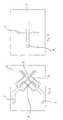
- the aperture 3 may thus be of any suitable form, and comprises in its simplest embodiment just a simple, straight slot, as is shown in figure 2b .
- the aperture feed 4 may then also, as is shown in figure 2b , be of an equally simple design, namely just a straight conductor 4.
- an aperture 3 comprises more commonly, as is shown in figure 2a , a pair of rectilinear slots 3 oriented at right angles to each other, so as to provide for double polarization operation.
- the aperture feed 4 may be fork-shaped, in order to be able to feed both aperture 3 slots in an efficient manner.
- the aperture feeds 4, 4' are placed on top of each other, however without being in contact to each other.
- the uppermost aperture feed 4 should thus have a shape permitting such configuration; more specifically, the aperture feed 4 that is placed on top of another aperture feed 4' should have some kind of curvature so that the bottom aperture feed 4' find room underneath the uppermost aperture feed 4, without them being in contact with each other.
- aperture slots could be designed in such way that the coupling there between is minimized.
- the design of the aperture(s) 3 may thus be such that the desired antenna characteristics are achieved.
- the reflector 2 is provided with holes into which a part of a snap joint element 5a is placed.
- the aperture feed 4 also provided with holes, is then placed between said snap joint element 5a and a complementary snap joint element 5b, whereby a very easily attachable fastening means is provided.
- the aperture feed 4 may also be removed in an easy manner, if desired.
- the assembly of the aperture antenna is thus greatly simplified compared to prior art antenna designs.
- the snap joint elements 5a, 5b should be of a non-conducting material, such as plastic, and the thickness H of the snap joint elements 5a, 5b be dimensioned so that optimal antenna characteristics are provided.
- the snap joint elements 5a, 5b may be disassembled, they may easily be replaced, whereby the thickness H may conveniently be altered, if desired, by replacing the snap joint elements 5a, 5b with snap joint elements of a different thickness H.
- Other fastening means are of course also possible, for example rivets, screws etc.
- the feeding network comprising feeding means 11, for example cables, for feeding the aperture antenna element 1 in accordance with the present invention.
- Each aperture antenna element 1 is feed by the feeding network, and thus connected to it by some suitable coupling means 12.
- the feeding network may be a conventional feeding network well known within the art.
- the aperture antenna 10 comprises one or several aperture antenna elements 1 in accordance with the present invention.
- the aperture antenna 10 further preferably comprises equally many patches 7, for providing an aperture-coupled wide-band antenna.
- the present invention provides an improved aperture antenna element, having a simpler design and a less expensive production compared to the prior art aperture antennas.
Landscapes
- Physics & Mathematics (AREA)
- Electromagnetism (AREA)
- Aerials With Secondary Devices (AREA)
- Variable-Direction Aerials And Aerial Arrays (AREA)
- Waveguide Aerials (AREA)
Description
- The present invention relates to aperture antennas, of the kind apparent from the preamble of the attached claim 1.
- Aperture antennas, such as for example slots, horns and aperture coupled patch antennas, are quite different in nature compared to dipole antennas. For example, in an aperture antenna, the electromagnetic radiation may be viewed as emanating from an aperture in a conducting enclosure. In the case of an aperture-coupled patch antenna the radiating patches are not conductively connected to the feeding arrangement, but excited by fields from an aperture.
- In contrast to this, a dipole antenna consists of two dipole arms conductively connected to the feedline, often via a balun. Furthermore, the radiation from an aperture antenna and a dipole, respectively, is totally different in their characteristics.
- The use of aperture antenna and dipole antennas, respectively, thus entails altogether different problems, and entails in particular totally different construction design aspects.
- Basically, a typical aperture antenna, or aperture radiator, comprises a waveguide (antenna feed line) at the end of which an aperture is placed. A reflector may be used to accentuate certain desired radiation characteristics. An example of an antenna based on the aperture antenna technique is an aperture coupled patch antenna.
- In accordance with the state of the art, a typical aperture coupled patch antenna comprises a dielectric laminate, for example a PCB (Printed Circuit Board). A feeding network, including an aperture feed feeding the antenna elements, is provided on one side of said PCB, typically by means of etching. The laminate is further provided with an electrically conductive layer on the opposite side serving as a ground plane for the aperture feed. The conductive layer may also serve as the ground plane for the antenna. The distance between the feeding network and the ground plane is thus fixed, whereby the antenna characteristics are reliable and predictable.
-
US 6,054,953 shows an example of a state of the art aperture-coupled antenna. The antenna described in this patent comprises a ground layer made of an electrically conductive material and is provided with a centrally located aperture. The aperture is etched on a substrate layer placed underneath the ground plane layer, and radiating patches are fed with microwave power from a feed network. -
US 4,847,625 shows another example of an state of the art aperture coupled antenna. Again, the feed layer is designed from a dielectric material, such as foam or a cladded material, including an etched strip forming the feedline. - However, the use of laminate, such as PCB, is very expensive, especially considering that the laminate should be made as thin as possible in order to reduce the amount of dielectric losses. Further, the use of laminate with an etched-on feeding network requires several manufacturing steps. There is, for example, a lot of soldering steps required, which besides the laborious work, causes other problems such as giving undesired intermodulation effects. Further still, the step of attaching the ground layer to the reflector may also be a rather tedious and time-consuming manufacturing step.
- Thus there exists a need for an improved aperture antenna, that is less expensive and that gives an easier and faster manufacturing method.
- An object of the present invention is to provide an antenna construction that overcomes the above mentioned disadvantages. It is an object of the invention to provide a new, inventive and simpler design of an aperture antenna. In particular, it is an object of the invention to provide an aperture antenna in which the use of expensive dielectric laminates is eliminated, whereby also the laborious etching steps are eliminated, and thereby giving a less expensive antenna.
- This object is achieved, according to a first aspect of the invention, by an aperture antenna as defined in the characterizing portion of claim 1.
- In accordance with the invention, an aperture antenna is provided, comprising a ground plane, an aperture feed and a reflector. The aperture antenna comprises at least one aperture, provided directly on the ground plane, wherein the ground plane also is the reflector of the antenna. Further, the aperture feed is separated from the ground plane and comprises a sheet metal element, and wherein the aperture feed is fastened to the reflector by snap joint elements.
- Such sheet metal element may be punched out, etched, water cut, milled or laser cut of the like. Thereby a non-expensive, but still efficient and reliable aperture feed is provided, which is easy to manufacture.
- In accordance with another embodiment of the aperture antenna of the invention, the aperture feed is fastened underneath said ground plane by means of distance elements. Thereby a predetermined, fixed distance between the ground plane of the antenna and the aperture feed is achieved in a simple and non-expensive way, giving the desired antenna properties. The distance may be altered, if needed, by replacing the distance elements with elements having a different thickness, thereby providing the antenna designer a flexible design means.
- In accordance with another embodiment of the aperture antenna of the invention, the aperture antenna is coupled to at least one apertured patch or non-apertured patch. The present invention may thus easily be implemented as an aperture-coupled patch antenna, giving a widely used aperture antenna.
- In accordance with another embodiment of the aperture antenna of the invention, it further comprises a shielding case fastened underneath the reflector and enclosing the end part of the aperture feed. This prevents, or at least minimizes, the back radiation, which is highly undesired for example in sector antennas, thereby minimizing losses and yielding a higher performance of the antenna.
- In accordance with another embodiment of the aperture antenna of the invention, the at least one aperture has an optional design. The aperture may be a straight slot aperture, a cross-shaped aperture consisting of perpendicular slots or an elliptic aperture. This provides an antenna that may easily be produced for its specific, intended use, and thus flexible design means.
- The present invention also relates to such a aperture antenna, whereby equivalent advantages are obtained.
- Further embodiments of the present invention and advantages of it will become clear in the following description.
-
-
Figure 1 shows a schematic overview over the inventive aperture antenna design in accordance with the present invention. -
Figure 2a shows a first exemplary embodiment of the reflector ground plane in accordance with the present invention. -
Figure 2b shows a second exemplary embodiment of the reflector ground plane in accordance with the present invention. -
Figures 3a and 3b show an exemplary embodiment for fastening the feeding network to the reflector ground plane. -
Figure 4 shows the coupling means for coupling a distributor main to the antenna part. -
Figure 5 shows an aperture antenna including the aperture antenna element in accordance with the present invention. - Throughout the description an aperture antenna element should be understood as comprising the parts involved directly in the radiation, unless otherwise stated. Thus, an aperture antenna element of the invention comprises an aperture feed, a reflector and at least one aperture. The aperture antenna element could optionally further include one or more patches and a shielding case preventing back radiation.
- The invention will now be described with reference first to
figure 1 , showing an overview over the inventive aperture antenna design in accordance with the present invention. Reference numeral 1 generally designates the aperture antenna element in accordance with the present invention, and the same reference numerals are used in all drawings for designating like elements. - The aperture antenna element 1 in accordance with the present invention comprises firstly a
reflector 2, which is made of an electrically conductive material, and which may have any desired shape, which may be adapted to its specific intended use. In accordance with the invention thereflector 2 also serves as the ground plane for the aperture feed. Thereflector 2 comprises one ormore apertures 3, which may be punched out, or water cut, laser cut or made by any other known method. Further, anaperture feed 4 is fastened to thereflector 2, for example by means ofdistance elements 5, made of a non-conducting material such as plastic. Theaperture feed 4 should be fastened in such a way that the distance between the reflector 2 (being also the ground plane) and theaperture feed 4 is equal at all points in order to guarantee the correct and desired antenna properties. Sufficientlymany distance elements 5, or other fastening means, should thus be provided in order to retain the distance. However, toomany distance elements 5 should not be used either, which would give an unnecessary tedious manufacturing step for fastening theaperture feed 4 to thereflector 2, and also yielding an unnecessary high cost. - The
aperture feed 4 may be any conducting element suitable for feeding power to the aperture(s) 3; it may for example be a sheet metal element or a metallized plastic. Theaperture feed 4 may be produced in any suitable way; it may for example be punched out from a metal sheet, laser cut, water cut, etched or milled. The distance from theaperture feed 4 to the ground plane (i.e. the reflector 2) is determined by the thickness of thedistance elements 5, and should be such that possible radiation losses from theaperture feed 4 are minimized. An exemplary distance, yielding acceptable antenna characteristics, lies within the range of 1-5 mm, forexample approximatively aperture feed 4 could be of any desired shape, examples of which are shown infigures 2a and 2b and described later. - The aperture antenna 1 may also comprise a
shielding case 6, used in order to prevent back radiation. Back radiation is highly undesired for example in sector antennas where all the radiation should be directed in a specific direction, and where any back radiation from one sector antenna could interfere with the radiation from another sector antenna. The shieldingcase 6 could be fastened to thereflector 2 by means of conducting adhesive tape, by means of rivets, or in any other suitable manner, in such a way that a conducting or non-conducting (capacitive coupling) fastening means is provided between the shieldingcase 6 and thereflector 2. - The shown aperture antenna 1 may be used as an aperture-coupled patch antenna, in which
case patches 7 should be included. Thepatches 7 may be of any known kind. The shape of the patches may be any suitable, such as rectangular, square, circular etc. Thepatches 7, if more than one, may be of different lengths, governing the characteristics of the antenna. Patches for compensating for the asymmetrical form of the ground plane may for example be provided. Further, apertured or non-apertured patches may be used, and such patches may also be combined in any desired manner. As is realised by a person skilled in the art, parasitic elements could also be included if desired, as is well known. - With reference now to
figures 2a and 2b , examples of possible configurations ofapertures 3 and aperture feeds 4 are shown. Theaperture 3 may thus be of any suitable form, and comprises in its simplest embodiment just a simple, straight slot, as is shown infigure 2b . Theaperture feed 4 may then also, as is shown infigure 2b , be of an equally simple design, namely just astraight conductor 4. However, anaperture 3 comprises more commonly, as is shown infigure 2a , a pair ofrectilinear slots 3 oriented at right angles to each other, so as to provide for double polarization operation. In this case theaperture feed 4 may be fork-shaped, in order to be able to feed bothaperture 3 slots in an efficient manner. It is also possible to provide for circular polarization operation, in which case, for example, a hybrid coupler could be used to accomplish the circular polarization operation, but as is well known within the art, there are other ways to accomplish the circular polarization such as by means of polarizers. As is outlined infigure 2a , the aperture feeds 4, 4' are placed on top of each other, however without being in contact to each other. Theuppermost aperture feed 4 should thus have a shape permitting such configuration; more specifically, theaperture feed 4 that is placed on top of another aperture feed 4' should have some kind of curvature so that the bottom aperture feed 4' find room underneath theuppermost aperture feed 4, without them being in contact with each other. Although only two examples of the aperture configuration are shown, a person skilled in the art realizes that various embodiments are possible. The aperture slots could be designed in such way that the coupling there between is minimized. The design of the aperture(s) 3 may thus be such that the desired antenna characteristics are achieved. - With reference now to
figures 3a and 3b an exemplary way for fastening theaperture feed 4 to thereflector 2 is shown. In the illustrated embodiment thereflector 2 is provided with holes into which a part of a snap joint element 5a is placed. Theaperture feed 4, also provided with holes, is then placed between said snap joint element 5a and a complementary snapjoint element 5b, whereby a very easily attachable fastening means is provided. Theaperture feed 4 may also be removed in an easy manner, if desired. The assembly of the aperture antenna is thus greatly simplified compared to prior art antenna designs. The snapjoint elements 5a, 5b should be of a non-conducting material, such as plastic, and the thickness H of the snapjoint elements 5a, 5b be dimensioned so that optimal antenna characteristics are provided. Since the snapjoint elements 5a, 5b may be disassembled, they may easily be replaced, whereby the thickness H may conveniently be altered, if desired, by replacing the snapjoint elements 5a, 5b with snap joint elements of a different thickness H. Other fastening means are of course also possible, for example rivets, screws etc. - With reference now to
figure 4 , the feeding network, comprising feeding means 11, for example cables, for feeding the aperture antenna element 1 in accordance with the present invention, is shown. Each aperture antenna element 1 is feed by the feeding network, and thus connected to it by some suitable coupling means 12. The feeding network may be a conventional feeding network well known within the art. - With reference finally to
figure 5 , anaperture antenna 10 in accordance with the present invention is shown. Theaperture antenna 10 comprises one or several aperture antenna elements 1 in accordance with the present invention. Theaperture antenna 10 further preferably comprises equallymany patches 7, for providing an aperture-coupled wide-band antenna. - To summarize, the present invention provides an improved aperture antenna element, having a simpler design and a less expensive production compared to the prior art aperture antennas. Although the present invention has been shown and described by specific embodiments, many alterations and modifications are possible, as would be obvious to a person skilled in the art.
Claims (8)
- An aperture antenna element comprising a ground plane, an aperture feed and a reflector, wherein at least one aperture (3) is provided directly in said ground plane, said ground plane also being said reflector (2), and wherein said aperture feed (4) is separated from said ground plane, characterized in that said aperture feed (4) comprises a sheet metal element and is fastened to said reflector (2) by snap joint elements (5a, 5b).
- Aperture antenna element as claimed in claim 1, wherein said aperture feed (4) is fastened underneath said ground plane by means of distance elements (5).
- Aperture antenna element as claimed in any of claims 1-2, wherein said aperture antenna element (1) is coupled to at least one apertured and/or non-apertured patch (7).
- Aperture antenna element as claimed in any of the preceding claims, wherein the aperture antenna element (1) further comprises a shielding case (6) fastened underneath the reflector (2) and enclosing the aperture feed (4).
- Aperture antenna element as claimed in any of the preceding claims, wherein said at least one aperture (3) has one of the following forms: a straight slot aperture, a cross-shaped aperture consisting of perpendicular slots or a elliptic aperture.
- Aperture antenna element as claimed in any of the preceding claims, wherein said at least one aperture (3) is fed with more than one aperture feed (4), thus providing dual polarization operation.
- Aperture antenna element as claimed in any of the preceding claims, wherein said aperture antenna element (1) further comprises circular polarization providing means.
- Aperture antenna characterized in that it comprises one or more aperture antenna elements (1) in accordance with any of claims 1-7, said aperture antenna further comprising one or more patches (7) aperture-coupled to a respective one of said aperture antenna element(s) (1).
Applications Claiming Priority (2)
| Application Number | Priority Date | Filing Date | Title |
|---|---|---|---|
| SE0401144A SE526492C2 (en) | 2004-05-03 | 2004-05-03 | Aperturantennelement |
| PCT/SE2005/000643 WO2005107008A1 (en) | 2004-05-03 | 2005-05-03 | Aperture antenna element |
Publications (2)
| Publication Number | Publication Date |
|---|---|
| EP1743397A1 EP1743397A1 (en) | 2007-01-17 |
| EP1743397B1 true EP1743397B1 (en) | 2013-07-24 |
Family
ID=32466197
Family Applications (1)
| Application Number | Title | Priority Date | Filing Date |
|---|---|---|---|
| EP05749908.9A Expired - Lifetime EP1743397B1 (en) | 2004-05-03 | 2005-05-03 | Aperture antenna element |
Country Status (4)
| Country | Link |
|---|---|
| EP (1) | EP1743397B1 (en) |
| CN (1) | CN1947303A (en) |
| SE (1) | SE526492C2 (en) |
| WO (1) | WO2005107008A1 (en) |
Families Citing this family (4)
| Publication number | Priority date | Publication date | Assignee | Title |
|---|---|---|---|---|
| EP1927156A2 (en) | 2005-09-19 | 2008-06-04 | Fractus, S.A. | Antenna set, portable wireless device, and use of a conductive element for tuning the ground-plane of the antenna set |
| US8120536B2 (en) | 2008-04-11 | 2012-02-21 | Powerwave Technologies Sweden Ab | Antenna isolation |
| US8085209B2 (en) * | 2009-04-02 | 2011-12-27 | Viasat, Inc. | Sub-array polarization control using rotated dual polarized radiating elements |
| CN101894990A (en) * | 2010-06-24 | 2010-11-24 | 东南大学 | Active Frequency Selective Surface with Polarization Insensitive Dual Frequency Feature |
Family Cites Families (5)
| Publication number | Priority date | Publication date | Assignee | Title |
|---|---|---|---|---|
| US4847625A (en) | 1988-02-16 | 1989-07-11 | Ford Aerospace Corporation | Wideband, aperture-coupled microstrip antenna |
| GB2308012B (en) * | 1995-12-05 | 1999-11-17 | Northern Telecom Ltd | A radiation shielding device |
| SE9603565D0 (en) * | 1996-05-13 | 1996-09-30 | Allgon Ab | Flat antenna |
| US6054953A (en) | 1998-12-10 | 2000-04-25 | Allgon Ab | Dual band antenna |
| WO2001041256A1 (en) * | 1999-12-01 | 2001-06-07 | Allgon Ab | An antenna assembly and a method of mounting an antenna assembly |
-
2004
- 2004-05-03 SE SE0401144A patent/SE526492C2/en not_active IP Right Cessation
-
2005
- 2005-05-03 WO PCT/SE2005/000643 patent/WO2005107008A1/en not_active Ceased
- 2005-05-03 EP EP05749908.9A patent/EP1743397B1/en not_active Expired - Lifetime
- 2005-05-03 CN CNA2005800130095A patent/CN1947303A/en active Pending
Also Published As
| Publication number | Publication date |
|---|---|
| SE0401144L (en) | 2005-09-27 |
| SE0401144D0 (en) | 2004-05-03 |
| WO2005107008A1 (en) | 2005-11-10 |
| WO2005107008A8 (en) | 2006-04-06 |
| SE526492C2 (en) | 2005-09-27 |
| CN1947303A (en) | 2007-04-11 |
| EP1743397A1 (en) | 2007-01-17 |
Similar Documents
| Publication | Publication Date | Title |
|---|---|---|
| US4719470A (en) | Broadband printed circuit antenna with direct feed | |
| US7026993B2 (en) | Planar antenna and array antenna | |
| US5400041A (en) | Radiating element incorporating impedance transformation capabilities | |
| EP1493204B1 (en) | Multi-band planar antenna | |
| EP0188345A2 (en) | Dual frequency band antenna system | |
| WO2019113282A1 (en) | Dipole antenna | |
| CN1336024A (en) | Antenna assembly | |
| US10978812B2 (en) | Single layer shared aperture dual band antenna | |
| US6483476B2 (en) | One-piece Yagi-Uda antenna and process for making the same | |
| JP2009060217A (en) | Tag antenna and tag | |
| TW200405613A (en) | Broadband couple-fed planar antennas with coupled metal strips on the ground plane | |
| US6788266B2 (en) | Diversity slot antenna | |
| US10680339B2 (en) | Low profile omnidirectional ceiling mount multiple-input multiple-output (MIMO) antennas | |
| CN109219906A (en) | Antenna assembly | |
| US8878742B1 (en) | Dipole with an unbalanced microstrip feed | |
| JP2002330024A (en) | Slot antenna | |
| EP3154125B1 (en) | Eight-frequency band antenna | |
| US20100141532A1 (en) | Antenna feeding arrangement | |
| EP1743397A1 (en) | Aperture antenna element | |
| CN116315655B (en) | Antenna and electronic equipment | |
| US20090079659A1 (en) | Multi-mode resonant wideband antenna | |
| JP2002290144A (en) | Planar array antenna | |
| WO1996010276A1 (en) | Ring microstrip antenna array | |
| KR20150011711A (en) | Wide-band patch antenna having double feeding technique and method of manufacturing the same | |
| EP3934023A1 (en) | Antenna element and antenna comprising antenna elements |
Legal Events
| Date | Code | Title | Description |
|---|---|---|---|
| PUAI | Public reference made under article 153(3) epc to a published international application that has entered the european phase |
Free format text: ORIGINAL CODE: 0009012 |
|
| 17P | Request for examination filed |
Effective date: 20060912 |
|
| AK | Designated contracting states |
Kind code of ref document: A1 Designated state(s): AT BE BG CH CY CZ DE DK EE ES FI FR GB GR HU IE IS IT LI LT LU MC NL PL PT RO SE SI SK TR |
|
| DAX | Request for extension of the european patent (deleted) | ||
| 17Q | First examination report despatched |
Effective date: 20071228 |
|
| REG | Reference to a national code |
Ref country code: DE Ref legal event code: R079 Ref document number: 602005040544 Country of ref document: DE Free format text: PREVIOUS MAIN CLASS: H01Q0001380000 Ipc: H01Q0009040000 |
|
| RIC1 | Information provided on ipc code assigned before grant |
Ipc: H01Q 21/26 20060101ALI20120830BHEP Ipc: H01Q 13/10 20060101ALI20120830BHEP Ipc: H01Q 9/04 20060101AFI20120830BHEP |
|
| GRAP | Despatch of communication of intention to grant a patent |
Free format text: ORIGINAL CODE: EPIDOSNIGR1 |
|
| GRAS | Grant fee paid |
Free format text: ORIGINAL CODE: EPIDOSNIGR3 |
|
| GRAA | (expected) grant |
Free format text: ORIGINAL CODE: 0009210 |
|
| AK | Designated contracting states |
Kind code of ref document: B1 Designated state(s): AT BE BG CH CY CZ DE DK EE ES FI FR GB GR HU IE IS IT LI LT LU MC NL PL PT RO SE SI SK TR |
|
| REG | Reference to a national code |
Ref country code: GB Ref legal event code: FG4D |
|
| REG | Reference to a national code |
Ref country code: DE Ref legal event code: R081 Ref document number: 602005040544 Country of ref document: DE Owner name: INTEL CORP., SANTA CLARA, US Free format text: FORMER OWNER: POWER TECHNOLOGIES SWEDEN AB, TAEBY, SE |
|
| REG | Reference to a national code |
Ref country code: CH Ref legal event code: EP |
|
| REG | Reference to a national code |
Ref country code: AT Ref legal event code: REF Ref document number: 623894 Country of ref document: AT Kind code of ref document: T Effective date: 20130815 |
|
| REG | Reference to a national code |
Ref country code: IE Ref legal event code: FG4D |
|
| REG | Reference to a national code |
Ref country code: DE Ref legal event code: R096 Ref document number: 602005040544 Country of ref document: DE Effective date: 20130919 |
|
| REG | Reference to a national code |
Ref country code: AT Ref legal event code: MK05 Ref document number: 623894 Country of ref document: AT Kind code of ref document: T Effective date: 20130724 |
|
| REG | Reference to a national code |
Ref country code: NL Ref legal event code: VDEP Effective date: 20130724 |
|
| REG | Reference to a national code |
Ref country code: LT Ref legal event code: MG4D |
|
| PG25 | Lapsed in a contracting state [announced via postgrant information from national office to epo] |
Ref country code: LT Free format text: LAPSE BECAUSE OF FAILURE TO SUBMIT A TRANSLATION OF THE DESCRIPTION OR TO PAY THE FEE WITHIN THE PRESCRIBED TIME-LIMIT Effective date: 20130724 Ref country code: SE Free format text: LAPSE BECAUSE OF FAILURE TO SUBMIT A TRANSLATION OF THE DESCRIPTION OR TO PAY THE FEE WITHIN THE PRESCRIBED TIME-LIMIT Effective date: 20130724 Ref country code: PT Free format text: LAPSE BECAUSE OF FAILURE TO SUBMIT A TRANSLATION OF THE DESCRIPTION OR TO PAY THE FEE WITHIN THE PRESCRIBED TIME-LIMIT Effective date: 20131125 Ref country code: AT Free format text: LAPSE BECAUSE OF FAILURE TO SUBMIT A TRANSLATION OF THE DESCRIPTION OR TO PAY THE FEE WITHIN THE PRESCRIBED TIME-LIMIT Effective date: 20130724 Ref country code: CY Free format text: LAPSE BECAUSE OF FAILURE TO SUBMIT A TRANSLATION OF THE DESCRIPTION OR TO PAY THE FEE WITHIN THE PRESCRIBED TIME-LIMIT Effective date: 20130717 Ref country code: IS Free format text: LAPSE BECAUSE OF FAILURE TO SUBMIT A TRANSLATION OF THE DESCRIPTION OR TO PAY THE FEE WITHIN THE PRESCRIBED TIME-LIMIT Effective date: 20131124 Ref country code: BE Free format text: LAPSE BECAUSE OF FAILURE TO SUBMIT A TRANSLATION OF THE DESCRIPTION OR TO PAY THE FEE WITHIN THE PRESCRIBED TIME-LIMIT Effective date: 20130724 |
|
| PG25 | Lapsed in a contracting state [announced via postgrant information from national office to epo] |
Ref country code: NL Free format text: LAPSE BECAUSE OF FAILURE TO SUBMIT A TRANSLATION OF THE DESCRIPTION OR TO PAY THE FEE WITHIN THE PRESCRIBED TIME-LIMIT Effective date: 20130724 Ref country code: SI Free format text: LAPSE BECAUSE OF FAILURE TO SUBMIT A TRANSLATION OF THE DESCRIPTION OR TO PAY THE FEE WITHIN THE PRESCRIBED TIME-LIMIT Effective date: 20130724 Ref country code: GR Free format text: LAPSE BECAUSE OF FAILURE TO SUBMIT A TRANSLATION OF THE DESCRIPTION OR TO PAY THE FEE WITHIN THE PRESCRIBED TIME-LIMIT Effective date: 20131025 Ref country code: PL Free format text: LAPSE BECAUSE OF FAILURE TO SUBMIT A TRANSLATION OF THE DESCRIPTION OR TO PAY THE FEE WITHIN THE PRESCRIBED TIME-LIMIT Effective date: 20130724 Ref country code: FI Free format text: LAPSE BECAUSE OF FAILURE TO SUBMIT A TRANSLATION OF THE DESCRIPTION OR TO PAY THE FEE WITHIN THE PRESCRIBED TIME-LIMIT Effective date: 20130724 |
|
| PG25 | Lapsed in a contracting state [announced via postgrant information from national office to epo] |
Ref country code: CY Free format text: LAPSE BECAUSE OF FAILURE TO SUBMIT A TRANSLATION OF THE DESCRIPTION OR TO PAY THE FEE WITHIN THE PRESCRIBED TIME-LIMIT Effective date: 20130724 |
|
| PG25 | Lapsed in a contracting state [announced via postgrant information from national office to epo] |
Ref country code: RO Free format text: LAPSE BECAUSE OF FAILURE TO SUBMIT A TRANSLATION OF THE DESCRIPTION OR TO PAY THE FEE WITHIN THE PRESCRIBED TIME-LIMIT Effective date: 20130724 Ref country code: SK Free format text: LAPSE BECAUSE OF FAILURE TO SUBMIT A TRANSLATION OF THE DESCRIPTION OR TO PAY THE FEE WITHIN THE PRESCRIBED TIME-LIMIT Effective date: 20130724 Ref country code: CZ Free format text: LAPSE BECAUSE OF FAILURE TO SUBMIT A TRANSLATION OF THE DESCRIPTION OR TO PAY THE FEE WITHIN THE PRESCRIBED TIME-LIMIT Effective date: 20130724 Ref country code: DK Free format text: LAPSE BECAUSE OF FAILURE TO SUBMIT A TRANSLATION OF THE DESCRIPTION OR TO PAY THE FEE WITHIN THE PRESCRIBED TIME-LIMIT Effective date: 20130724 Ref country code: EE Free format text: LAPSE BECAUSE OF FAILURE TO SUBMIT A TRANSLATION OF THE DESCRIPTION OR TO PAY THE FEE WITHIN THE PRESCRIBED TIME-LIMIT Effective date: 20130724 |
|
| PG25 | Lapsed in a contracting state [announced via postgrant information from national office to epo] |
Ref country code: ES Free format text: LAPSE BECAUSE OF FAILURE TO SUBMIT A TRANSLATION OF THE DESCRIPTION OR TO PAY THE FEE WITHIN THE PRESCRIBED TIME-LIMIT Effective date: 20130724 Ref country code: IT Free format text: LAPSE BECAUSE OF FAILURE TO SUBMIT A TRANSLATION OF THE DESCRIPTION OR TO PAY THE FEE WITHIN THE PRESCRIBED TIME-LIMIT Effective date: 20130724 |
|
| PLBE | No opposition filed within time limit |
Free format text: ORIGINAL CODE: 0009261 |
|
| STAA | Information on the status of an ep patent application or granted ep patent |
Free format text: STATUS: NO OPPOSITION FILED WITHIN TIME LIMIT |
|
| 26N | No opposition filed |
Effective date: 20140425 |
|
| REG | Reference to a national code |
Ref country code: DE Ref legal event code: R097 Ref document number: 602005040544 Country of ref document: DE Effective date: 20140425 |
|
| PG25 | Lapsed in a contracting state [announced via postgrant information from national office to epo] |
Ref country code: LU Free format text: LAPSE BECAUSE OF FAILURE TO SUBMIT A TRANSLATION OF THE DESCRIPTION OR TO PAY THE FEE WITHIN THE PRESCRIBED TIME-LIMIT Effective date: 20140503 |
|
| REG | Reference to a national code |
Ref country code: CH Ref legal event code: PL |
|
| PG25 | Lapsed in a contracting state [announced via postgrant information from national office to epo] |
Ref country code: MC Free format text: LAPSE BECAUSE OF FAILURE TO SUBMIT A TRANSLATION OF THE DESCRIPTION OR TO PAY THE FEE WITHIN THE PRESCRIBED TIME-LIMIT Effective date: 20130724 Ref country code: LI Free format text: LAPSE BECAUSE OF NON-PAYMENT OF DUE FEES Effective date: 20140531 Ref country code: CH Free format text: LAPSE BECAUSE OF NON-PAYMENT OF DUE FEES Effective date: 20140531 |
|
| REG | Reference to a national code |
Ref country code: IE Ref legal event code: MM4A |
|
| PG25 | Lapsed in a contracting state [announced via postgrant information from national office to epo] |
Ref country code: IE Free format text: LAPSE BECAUSE OF NON-PAYMENT OF DUE FEES Effective date: 20140503 |
|
| REG | Reference to a national code |
Ref country code: FR Ref legal event code: PLFP Year of fee payment: 12 |
|
| PG25 | Lapsed in a contracting state [announced via postgrant information from national office to epo] |
Ref country code: BG Free format text: LAPSE BECAUSE OF FAILURE TO SUBMIT A TRANSLATION OF THE DESCRIPTION OR TO PAY THE FEE WITHIN THE PRESCRIBED TIME-LIMIT Effective date: 20130724 |
|
| REG | Reference to a national code |
Ref country code: DE Ref legal event code: R081 Ref document number: 602005040544 Country of ref document: DE Owner name: INTEL CORP., SANTA CLARA, US Free format text: FORMER OWNER: POWERWAVE TECHNOLOGIES SWEDEN AB, TAEBY, SE |
|
| REG | Reference to a national code |
Ref country code: FR Ref legal event code: TP Owner name: INTEL CORPORATION, US Effective date: 20160606 Ref country code: FR Ref legal event code: TP Owner name: INTEL CORPORATION, US Effective date: 20160603 |
|
| PG25 | Lapsed in a contracting state [announced via postgrant information from national office to epo] |
Ref country code: TR Free format text: LAPSE BECAUSE OF FAILURE TO SUBMIT A TRANSLATION OF THE DESCRIPTION OR TO PAY THE FEE WITHIN THE PRESCRIBED TIME-LIMIT Effective date: 20130724 Ref country code: HU Free format text: LAPSE BECAUSE OF FAILURE TO SUBMIT A TRANSLATION OF THE DESCRIPTION OR TO PAY THE FEE WITHIN THE PRESCRIBED TIME-LIMIT; INVALID AB INITIO Effective date: 20050503 |
|
| PGFP | Annual fee paid to national office [announced via postgrant information from national office to epo] |
Ref country code: GB Payment date: 20160427 Year of fee payment: 12 |
|
| REG | Reference to a national code |
Ref country code: GB Ref legal event code: 732E Free format text: REGISTERED BETWEEN 20160707 AND 20160713 |
|
| PGFP | Annual fee paid to national office [announced via postgrant information from national office to epo] |
Ref country code: FR Payment date: 20160426 Year of fee payment: 12 |
|
| REG | Reference to a national code |
Ref country code: GB Ref legal event code: 732E Free format text: REGISTERED BETWEEN 20160811 AND 20160817 |
|
| REG | Reference to a national code |
Ref country code: GB Ref legal event code: 732E Free format text: REGISTERED BETWEEN 20161013 AND 20161019 |
|
| GBPC | Gb: european patent ceased through non-payment of renewal fee |
Effective date: 20170503 |
|
| REG | Reference to a national code |
Ref country code: FR Ref legal event code: ST Effective date: 20180131 |
|
| PG25 | Lapsed in a contracting state [announced via postgrant information from national office to epo] |
Ref country code: GB Free format text: LAPSE BECAUSE OF NON-PAYMENT OF DUE FEES Effective date: 20170503 |
|
| PG25 | Lapsed in a contracting state [announced via postgrant information from national office to epo] |
Ref country code: FR Free format text: LAPSE BECAUSE OF NON-PAYMENT OF DUE FEES Effective date: 20170531 |
|
| PGFP | Annual fee paid to national office [announced via postgrant information from national office to epo] |
Ref country code: DE Payment date: 20200422 Year of fee payment: 16 |
|
| REG | Reference to a national code |
Ref country code: DE Ref legal event code: R119 Ref document number: 602005040544 Country of ref document: DE |
|
| PG25 | Lapsed in a contracting state [announced via postgrant information from national office to epo] |
Ref country code: DE Free format text: LAPSE BECAUSE OF NON-PAYMENT OF DUE FEES Effective date: 20211201 |