EP1739958A1 - Electronic device and image capture module thereof - Google Patents
Electronic device and image capture module thereof Download PDFInfo
- Publication number
- EP1739958A1 EP1739958A1 EP06009237A EP06009237A EP1739958A1 EP 1739958 A1 EP1739958 A1 EP 1739958A1 EP 06009237 A EP06009237 A EP 06009237A EP 06009237 A EP06009237 A EP 06009237A EP 1739958 A1 EP1739958 A1 EP 1739958A1
- Authority
- EP
- European Patent Office
- Prior art keywords
- camera unit
- opening
- image capture
- capture module
- housing
- Prior art date
- Legal status (The legal status is an assumption and is not a legal conclusion. Google has not performed a legal analysis and makes no representation as to the accuracy of the status listed.)
- Granted
Links
Images

Classifications
-
- G—PHYSICS
- G02—OPTICS
- G02B—OPTICAL ELEMENTS, SYSTEMS OR APPARATUS
- G02B27/00—Optical systems or apparatus not provided for by any of the groups G02B1/00 - G02B26/00, G02B30/00
- G02B27/0006—Optical systems or apparatus not provided for by any of the groups G02B1/00 - G02B26/00, G02B30/00 with means to keep optical surfaces clean, e.g. by preventing or removing dirt, stains, contamination, condensation
-
- G—PHYSICS
- G02—OPTICS
- G02B—OPTICAL ELEMENTS, SYSTEMS OR APPARATUS
- G02B13/00—Optical objectives specially designed for the purposes specified below
- G02B13/001—Miniaturised objectives for electronic devices, e.g. portable telephones, webcams, PDAs, small digital cameras
- G02B13/0015—Miniaturised objectives for electronic devices, e.g. portable telephones, webcams, PDAs, small digital cameras characterised by the lens design
- G02B13/002—Miniaturised objectives for electronic devices, e.g. portable telephones, webcams, PDAs, small digital cameras characterised by the lens design having at least one aspherical surface
- G02B13/003—Miniaturised objectives for electronic devices, e.g. portable telephones, webcams, PDAs, small digital cameras characterised by the lens design having at least one aspherical surface having two lenses
-
- G—PHYSICS
- G02—OPTICS
- G02B—OPTICAL ELEMENTS, SYSTEMS OR APPARATUS
- G02B7/00—Mountings, adjusting means, or light-tight connections, for optical elements
- G02B7/02—Mountings, adjusting means, or light-tight connections, for optical elements for lenses
- G02B7/021—Mountings, adjusting means, or light-tight connections, for optical elements for lenses for more than one lens
-
- H—ELECTRICITY
- H04—ELECTRIC COMMUNICATION TECHNIQUE
- H04N—PICTORIAL COMMUNICATION, e.g. TELEVISION
- H04N23/00—Cameras or camera modules comprising electronic image sensors; Control thereof
- H04N23/50—Constructional details
- H04N23/54—Mounting of pick-up tubes, electronic image sensors, deviation or focusing coils
-
- H—ELECTRICITY
- H04—ELECTRIC COMMUNICATION TECHNIQUE
- H04N—PICTORIAL COMMUNICATION, e.g. TELEVISION
- H04N23/00—Cameras or camera modules comprising electronic image sensors; Control thereof
- H04N23/57—Mechanical or electrical details of cameras or camera modules specially adapted for being embedded in other devices
Definitions
- the invention relates to an electronic device and an image capture module thereof and, in particular, to an electronic device and an image capture module thereof that are designed for preventing particles pollution.
- photograph function is not only carried out in digital cameras and video recorders but also in portable communication devices extensively.
- portable communication devices with the photograph function are a main tendency in the market.
- the conventional portable communication device having photograph function utilizes an image capture module to capture an image of object. Then, image information is recorded on a recording medium.
- the conventional image capture module 1 includes a housing 10, a camera unit 11, and a sensor 12.
- the housing 10 is formed with a front cover 101 and a rear cover 102.
- the front cover 101 has an opening 101A.
- the camera unit 11 including a barrel 111 and a lens assembly 112 is accommodated in the housing 10.
- the barrel 111 includes a container 1111 where the lens assembly 112 is accommodated. Therefore, the opening 101A of the front cover 101 exposes a portion of the camera unit 11.
- the sensor 12 is disposed between the camera unit 11 and housing 10 to receive a light beam passing the camera unit 11.
- the sensor 12 can be a charge coupled device (CCD) or a complementary metal oxide semiconductor sensor (CMOS).
- CCD charge coupled device
- CMOS complementary metal oxide semiconductor sensor
- the conventional image capture module 1 generally includes a focus system (not shown in the figure) and, in particular, when the focus system is an auto-focus system, the focus system can improve quality of the image picked up. Furthermore, the focus system includes a transmission element, which can drive the camera unit 11 close to or away from the opening 101A to reach an optimum position for focusing in accordance with the distance of the object placed.
- appropriate space 13 between the opening 101A of the housing 10 and the camera unit 11 is required to allow the camera unit 11 moving forwards and backwards, so that the camera unit 11 can smoothly move corresponding to the opening 101A,.
- the aforesaid space 13 may let the foreign tiny particles easily enter the image capture module 1 to affect the quality of the image picked up.
- the invention is to provide an electronic device and an image capture module thereof that are designed for blocking particles to enter themselves and having a shock absorbing ability.
- an image capture module of the invention includes a housing, a camera unit, and a shielding element.
- the housing has a first opening.
- the camera unit is accommodated in the housing and is adjacent to the first opening.
- the first opening exposes at lest one portion of the camera unit.
- the shielding element is disposed between the camera unit and the housing.
- the shielding element is disposed around the camera unit such that the shielding element and the camera unit cover the first opening.
- an electronic device of the invention includes an image capture module and a main body.
- the image capture module includes a housing, a camera unit, and a shielding element.
- the housing has a first opening.
- the camera unit is accommodated in the housing and is adjacent to the first opening.
- the first opening exposes at lest one portion of the camera unit.
- the shielding element is disposed between the camera unit and the housing.
- the shielding element is disposed around the camera unit such that the shielding element and the camera unit cover the first opening.
- the image capture module is accommodated in the main body.
- the main body has a second opening and a transparent cover.
- the second opening is correspondingly disposed with the first opening.
- the transparent cover covers the second opening.
- the electronic device and the image capture module thereof of the invention are by way of disposing a shielding element between the camera unit and the housing.
- the shielding element is disposed around the camera unit such that the shielding element and the camera unit covers the first opening of the housing. Due to no space between the housing and the camera unit, the foreign particles are prevented from entering into the image capture module.
- the shielding element can be elastic for absorbing the shock generated in the movement of the camera unit corresponding to the first opening. Therefore, the image capture module of the invention further has an absorbing shock effect.
- the surface of the shielding element can be designed for having a rough structure, such as a waved structure or a ladder structure. The rough structure is used to absorb or reflect the useless light beams for image generation so as to improve the quality of the image.
- the shielding element can be doped with mental particles to reduce interference of the electromagnetic wave.
- FIG. 1 is a schematic sectional view showing the conventional image capture module
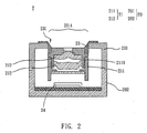
- FIG. 2 is a schematic sectional view showing an image capture module according to a preferred embodiment of the invention.
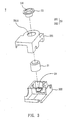
- FIG. 3 is a schematic exploded view showing an image capture module according to the preferred embodiment of the invention.
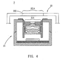
- FIG. 4 is a schematic sectional view showing an electronic device according to a preferred embodiment of the invention.
- an image capture module 2 includes a housing 20, a camera unit 21, and an elastic element 23.
- the elastic element 23 is as a shielding element disposing between the camera unit 21 and the housing 20.
- the hosing 20 includes a front cover 201 and a rear cover 202.
- the front cover 201 and the rear cover 202 are connected with each other to form the housing 20.
- the housing 20 has a first opening 201A, which is formed on the front cover 201 of the housing 20.
- the camera unit 21 is accommodated in the housing 20 and is adjacent to the first opening 201A.
- the first opening 201A exposes at least one portion of the camera unit 21.
- the camera unit 21 includes a barrel 211 and a lens assembly 212.
- the barrel 211 includes a container 2111 where the lens assembly 212 is accommodated.
- the lens assembly 212 has a plurality of lenses.
- the elastic element 23 is disposed between the camera unit 21 and housing 20.
- One portion of the elastic element 23 is connected to the housing 20 and the other portion of the elastic element 23 surrounds the camera unit 21.
- the front cover 201 of the housing 20 is connected with the camera unit 21 through the elastic element 23 such that the elastic element 23 and the camera unit 21 simultaneously cover the first opening 201A. Therefore, the hosing 20 and the camera unit 21 are tightly connected and have no space between them, so that the foreign particles are prohibited from entering into the image capture module 2.
- the elastic element 23 can be made of an elastic material such as rubber or plastic.
- the image capture module 2 does auto-focus process and the camera unit 21 moves corresponding to the first opening 201A.
- the elastic element 23 is compressed when the camera unit 21 is close to the first opening 201 A and the elastic element 23 is restored when the camera unit 21 is away from the first opening 201A.
- the elastic element 23 is provided for absorbing shock generated in the movement of the camera unit 21.
- a surface 231 of the elastic element 23, on which the light beam is incident has a rough structure such as a ladder structure (as shown in FIG. 2) or a waved structure. The rough structure can be integrately formed on the elastic element 23.
- the useless light for the image generation can be effectively reflected and absorbed by the aforesaid rough structure, and the opportunity for the useless light entering into the camera unit 21 can be reduced.
- the elastic element 23 can be doped with mental particles for impeding the interference of the electromagnetic wave.
- the image capture module 2 of the present embodiment further can include a sensor 24 accommodated in the housing 20 and disposed between the camera unit 21 and the housing 20.
- the sensor 24 is used to receive a light beam passing through the first opening 201 A and the camera unit 21 orderly and then generate an image.
- the sensor 24 can be a charge coupled device (CCD) or a complementary metal oxide semiconductor sensor (CMOS).
- the image capture module 2 of the present embodiment further includes a transmission element (not shown in the figure), which drives the camera unit 21 close to or away from the first opening 201A. That is, when the image capture module 2 progresses auto-focus process, the camera unit 21 is driven by the transmission element to move corresponding to the first opening 201A.
- FIG. 3 it is a schematic exploded view of showing the image capture module 2 according to the preferred embodiment of the invention.
- the sensor 24 is accommodated in the rear cover 202 of the housing 20.
- the camera unit 21 is corresponding disposed with sensor 24. At least one portion of the camera unit 21 is accommodated in the rear cover 202.
- the front cover 201 is connected with the rear cover 202 to completely contain the camera unit 21 into the housing 20.
- the front cover 201 has the first opening 201A disposed opposite to the camera unit 21. The light beam passes through the first opening 201 A and the camera unit 21 and finally arrives at the sensor 24 to generate an image.
- the elastic element 23 is disposed between the front cover 201 and the camera unit 21 so that there is no space between the housing 20 and the camera unit 21 and the foreign particle is effectively prohibited from entering into the image capture module 2. Moreover, the surface 231 of the elastic element 23 on which the light beam is incident has the rough structure to effectively reflect or absorb useless light from the outside.
- an electronic device 3 includes an image capture module 31 and a main body 32.
- the main body 32 has a second opening 321A and a transparent cover 322.
- the image capture module 31 is disposed in the main body 32.
- the second opening 321A is corresponding disposed with the first opening 31A.
- the transparent cover 322 covers the second opening 321.
- the electronic device 3 can be a mobile phone and the main body 32 can be the housing of the mobile phone. Certainly, the electronic device 3 also can be else electronic products having image capture function.
- the electronic device and the image capture module thereof of the invention are by way of disposing a shielding element between the camera unit and the housing.
- the shielding element is disposed around the camera unit such that the first opening of the housing is covered by the shielding element and the camera unit. Due to no space between the housing and the camera unit, the purpose of prohibiting the foreign particles from entering into the image capture module is achieved.
- the shielding element can be elastic for absorbing the shock generated in the movement of the camera unit corresponding to the first opening. Therefore, the image capture module of the invention further has a shock absorbing ability.
- the surface of the shielding element can be designed for having a rough structure, such as a waved structure or a ladder structure. The rough structure is used to absorb or reflect the useless light beams for image generation so as to improve the quality of the image.
- the shielding element can be doped with mental particles to reduce interference of the electromagnetic wave.
Landscapes
- Physics & Mathematics (AREA)
- General Physics & Mathematics (AREA)
- Optics & Photonics (AREA)
- Engineering & Computer Science (AREA)
- Multimedia (AREA)
- Signal Processing (AREA)
- Studio Devices (AREA)
- Camera Bodies And Camera Details Or Accessories (AREA)
Abstract
Description
- The invention relates to an electronic device and an image capture module thereof and, in particular, to an electronic device and an image capture module thereof that are designed for preventing particles pollution.
- With great progress in the technology, photograph function is not only carried out in digital cameras and video recorders but also in portable communication devices extensively. Nowadays, the portable communication devices with the photograph function are a main tendency in the market.
- The conventional portable communication device having photograph function utilizes an image capture module to capture an image of object. Then, image information is recorded on a recording medium. With reference to FIG. 1, the conventional image capture module 1 includes a housing 10, a
camera unit 11, and asensor 12. The housing 10 is formed with afront cover 101 and arear cover 102. In this case, thefront cover 101 has an opening 101A. Thecamera unit 11 including abarrel 111 and alens assembly 112 is accommodated in the housing 10. Thebarrel 111 includes a container 1111 where thelens assembly 112 is accommodated. Therefore, the opening 101A of thefront cover 101 exposes a portion of thecamera unit 11. Thesensor 12 is disposed between thecamera unit 11 and housing 10 to receive a light beam passing thecamera unit 11. Herein, thesensor 12 can be a charge coupled device (CCD) or a complementary metal oxide semiconductor sensor (CMOS). - The conventional image capture module 1 generally includes a focus system (not shown in the figure) and, in particular, when the focus system is an auto-focus system, the focus system can improve quality of the image picked up. Furthermore, the focus system includes a transmission element, which can drive the
camera unit 11 close to or away from the opening 101A to reach an optimum position for focusing in accordance with the distance of the object placed. - As mentioned above,
appropriate space 13 between the opening 101A of the housing 10 and thecamera unit 11 is required to allow thecamera unit 11 moving forwards and backwards, so that thecamera unit 11 can smoothly move corresponding to the opening 101A,. However, theaforesaid space 13 may let the foreign tiny particles easily enter the image capture module 1 to affect the quality of the image picked up. - Therefore, according to the above-mentioned problems of the state of the art, it is a subjective to provide an electronic device and an image capture module thereof that are designed for blocking particles to enter themselves
- In view of the foregoing, the invention is to provide an electronic device and an image capture module thereof that are designed for blocking particles to enter themselves and having a shock absorbing ability.
- To achieve the above, an image capture module of the invention includes a housing, a camera unit, and a shielding element. In this case, the housing has a first opening. The camera unit is accommodated in the housing and is adjacent to the first opening. The first opening exposes at lest one portion of the camera unit. The shielding element is disposed between the camera unit and the housing. The shielding element is disposed around the camera unit such that the shielding element and the camera unit cover the first opening.
- To achieve the above, an electronic device of the invention includes an image capture module and a main body. In this case, the image capture module includes a housing, a camera unit, and a shielding element. The housing has a first opening. The camera unit is accommodated in the housing and is adjacent to the first opening. The first opening exposes at lest one portion of the camera unit. The shielding element is disposed between the camera unit and the housing. The shielding element is disposed around the camera unit such that the shielding element and the camera unit cover the first opening. The image capture module is accommodated in the main body. The main body has a second opening and a transparent cover. The second opening is correspondingly disposed with the first opening. The transparent cover covers the second opening.
- As mentioned above, the electronic device and the image capture module thereof of the invention are by way of disposing a shielding element between the camera unit and the housing. Specially, the shielding element is disposed around the camera unit such that the shielding element and the camera unit covers the first opening of the housing. Due to no space between the housing and the camera unit, the foreign particles are prevented from entering into the image capture module. Moreover, the shielding element can be elastic for absorbing the shock generated in the movement of the camera unit corresponding to the first opening. Therefore, the image capture module of the invention further has an absorbing shock effect. In addition, the surface of the shielding element can be designed for having a rough structure, such as a waved structure or a ladder structure. The rough structure is used to absorb or reflect the useless light beams for image generation so as to improve the quality of the image. Furthermore, the shielding element can be doped with mental particles to reduce interference of the electromagnetic wave.
- The invention will become more fully understood from the detailed description given herein below illustration only, and thus is not limitative of the present invention, and wherein:
- FIG. 1 is a schematic sectional view showing the conventional image capture module;
- FIG. 2 is a schematic sectional view showing an image capture module according to a preferred embodiment of the invention;
- FIG. 3 is a schematic exploded view showing an image capture module according to the preferred embodiment of the invention; and
- FIG. 4 is a schematic sectional view showing an electronic device according to a preferred embodiment of the invention.
- The present invention will be apparent from the following detailed description, which proceeds with reference to the accompanying drawings, wherein the same references relate to the same elements.
- With reference to FIG. 2, an
image capture module 2 according to a preferred embodiment of the invention includes ahousing 20, acamera unit 21, and anelastic element 23. In the present embodiment, theelastic element 23 is as a shielding element disposing between thecamera unit 21 and thehousing 20. - As shown in FIG. 2, the
hosing 20 includes afront cover 201 and arear cover 202. Thefront cover 201 and therear cover 202 are connected with each other to form thehousing 20. Thehousing 20 has a first opening 201A, which is formed on thefront cover 201 of thehousing 20. Thecamera unit 21 is accommodated in thehousing 20 and is adjacent to the first opening 201A. Thefirst opening 201A exposes at least one portion of thecamera unit 21. - As mentioned above, the
camera unit 21 includes abarrel 211 and alens assembly 212. Thebarrel 211 includes acontainer 2111 where thelens assembly 212 is accommodated. Herein, thelens assembly 212 has a plurality of lenses. - The
elastic element 23 is disposed between thecamera unit 21 andhousing 20. One portion of theelastic element 23 is connected to thehousing 20 and the other portion of theelastic element 23 surrounds thecamera unit 21. With reference to FIG. 2, thefront cover 201 of thehousing 20 is connected with thecamera unit 21 through theelastic element 23 such that theelastic element 23 and thecamera unit 21 simultaneously cover thefirst opening 201A. Therefore, the hosing 20 and thecamera unit 21 are tightly connected and have no space between them, so that the foreign particles are prohibited from entering into theimage capture module 2. - In the present embodiment, the
elastic element 23 can be made of an elastic material such as rubber or plastic. Theimage capture module 2 does auto-focus process and thecamera unit 21 moves corresponding to thefirst opening 201A. Theelastic element 23 is compressed when thecamera unit 21 is close to thefirst opening 201 A and theelastic element 23 is restored when thecamera unit 21 is away from thefirst opening 201A. In such manner, theelastic element 23 is provided for absorbing shock generated in the movement of thecamera unit 21. Moreover, in the present embodiment, asurface 231 of theelastic element 23, on which the light beam is incident, has a rough structure such as a ladder structure (as shown in FIG. 2) or a waved structure. The rough structure can be integrately formed on theelastic element 23. Therefore, the useless light for the image generation can be effectively reflected and absorbed by the aforesaid rough structure, and the opportunity for the useless light entering into thecamera unit 21 can be reduced. Additionally, theelastic element 23 can be doped with mental particles for impeding the interference of the electromagnetic wave. - The
image capture module 2 of the present embodiment further can include asensor 24 accommodated in thehousing 20 and disposed between thecamera unit 21 and thehousing 20. Thesensor 24 is used to receive a light beam passing through thefirst opening 201 A and thecamera unit 21 orderly and then generate an image. In the present embodiment, thesensor 24 can be a charge coupled device (CCD) or a complementary metal oxide semiconductor sensor (CMOS). - Additionally, the
image capture module 2 of the present embodiment further includes a transmission element (not shown in the figure), which drives thecamera unit 21 close to or away from thefirst opening 201A. That is, when theimage capture module 2 progresses auto-focus process, thecamera unit 21 is driven by the transmission element to move corresponding to thefirst opening 201A. - With reference to FIG. 3 for fully understand the content of the invention, it is a schematic exploded view of showing the
image capture module 2 according to the preferred embodiment of the invention. Thesensor 24 is accommodated in therear cover 202 of thehousing 20. Thecamera unit 21 is corresponding disposed withsensor 24. At least one portion of thecamera unit 21 is accommodated in therear cover 202. Thefront cover 201 is connected with therear cover 202 to completely contain thecamera unit 21 into thehousing 20. Thefront cover 201 has thefirst opening 201A disposed opposite to thecamera unit 21. The light beam passes through thefirst opening 201 A and thecamera unit 21 and finally arrives at thesensor 24 to generate an image. Theelastic element 23 is disposed between thefront cover 201 and thecamera unit 21 so that there is no space between thehousing 20 and thecamera unit 21 and the foreign particle is effectively prohibited from entering into theimage capture module 2. Moreover, thesurface 231 of theelastic element 23 on which the light beam is incident has the rough structure to effectively reflect or absorb useless light from the outside. - In addition, with reference to FIG. 4, an
electronic device 3 according to a preferred embodiment of the invention includes animage capture module 31 and amain body 32. - Due to the structure, disposition, and function of the
image capture module 31 are the same as those mentioned above, so the detailed description are omitted herein. - The
main body 32 has asecond opening 321A and atransparent cover 322. Theimage capture module 31 is disposed in themain body 32. Thesecond opening 321A is corresponding disposed with thefirst opening 31A. Thetransparent cover 322 covers the second opening 321. In the present embodiment, theelectronic device 3 can be a mobile phone and themain body 32 can be the housing of the mobile phone. Certainly, theelectronic device 3 also can be else electronic products having image capture function. - In conclusion, the electronic device and the image capture module thereof of the invention are by way of disposing a shielding element between the camera unit and the housing. Specially, the shielding element is disposed around the camera unit such that the first opening of the housing is covered by the shielding element and the camera unit. Due to no space between the housing and the camera unit, the purpose of prohibiting the foreign particles from entering into the image capture module is achieved. Moreover, the shielding element can be elastic for absorbing the shock generated in the movement of the camera unit corresponding to the first opening. Therefore, the image capture module of the invention further has a shock absorbing ability. In addition, the surface of the shielding element can be designed for having a rough structure, such as a waved structure or a ladder structure. The rough structure is used to absorb or reflect the useless light beams for image generation so as to improve the quality of the image. Furthermore, the shielding element can be doped with mental particles to reduce interference of the electromagnetic wave.
- Although the invention has been described with reference to specific embodiments, this description is not meant to be construed in a limiting sense. Various modifications of the disclosed embodiments, as well as alternative embodiments, will be apparent to persons skilled in the art. It is, therefore, contemplated that the appended claims will cover all modifications that fall within the true scope of the invention.
Claims (11)
- An image capture module, comprising:a housing, which has a first opening;a camera unit, which is accommodated in the housing and is adjacent to the first opening, wherein the first opening exposes at least one portion of the camera unit; anda shielding element, which is disposed between the camera unit and the housing,wherein the shielding element is disposed around the camera unit such that the shielding element and the camera unit cover the first opening.
- The image capture module of claim 1, wherein the camera unit comprises a barrel and a lens assembly, the barrel comprises a container where the lens assembly is accommodated.
- The image capture module of claim 1, wherein the surface of the shielding element has a rough structure.
- The image capture module of claim 1, wherein the surface of the shielding element has a ladder structure.
- The image capture module of claim 1, wherein the surface of the shielding element has a waved structure.
- The image capture module of claim 1, wherein the shielding element is an elastic element.
- The image capture module of claim 6, wherein the elastic element is made of rubber or plastic.
- The image capture module of claim 1, wherein the shielding element is doped with mental particles.
- The image capture module of claim 1, further comprising:a sensor, which is accommodated in the housing and is used to receive a light beam passing through the camera unit.
- The image capture module of claim 1, further comprising:a transmission element, which drives the camera unit close to or away from the first opening.
- An electronic device, comprising:an image capture module, which comprises a housing, a camera unit, and a shielding element, the housing has a first opening, the camera unit is accommodated in the housing and is adjacent to the first opening, the first opening exposes at least one portion of the camera unit, and the shielding element is disposed between the camera unit and the housing, wherein the shielding element is disposed around the camera unit such that the shielding element and the camera unit cover the first opening; anda main body, which the image capture module is accommodated in, wherein the main body has a second opening and a transparent cover, the second opening is correspondingly disposed with the first opening, and the transparent cover covers the second opening.
Applications Claiming Priority (1)
| Application Number | Priority Date | Filing Date | Title |
|---|---|---|---|
| CNB2005100802677A CN100470349C (en) | 2005-06-28 | 2005-06-28 | Image acquisition module |
Publications (2)
| Publication Number | Publication Date |
|---|---|
| EP1739958A1 true EP1739958A1 (en) | 2007-01-03 |
| EP1739958B1 EP1739958B1 (en) | 2009-07-08 |
Family
ID=36754653
Family Applications (1)
| Application Number | Title | Priority Date | Filing Date |
|---|---|---|---|
| EP06009237A Expired - Lifetime EP1739958B1 (en) | 2005-06-28 | 2006-05-04 | Electronic device and image capture module thereof |
Country Status (3)
| Country | Link |
|---|---|
| EP (1) | EP1739958B1 (en) |
| CN (1) | CN100470349C (en) |
| DE (1) | DE602006007645D1 (en) |
Cited By (2)
| Publication number | Priority date | Publication date | Assignee | Title |
|---|---|---|---|---|
| EP3537207A4 (en) * | 2016-11-07 | 2020-04-29 | Kyocera Corporation | IMAGE DISPLAY DEVICE |
| WO2024196519A1 (en) * | 2023-03-22 | 2024-09-26 | Tusimple, Inc. | Apparatus, system, and method for sensor housing |
Families Citing this family (7)
| Publication number | Priority date | Publication date | Assignee | Title |
|---|---|---|---|---|
| CN103091941B (en) * | 2011-10-27 | 2015-09-30 | 亚洲光学股份有限公司 | Lenses with photosensitive element retraction function |
| CN104471923A (en) * | 2012-04-13 | 2015-03-25 | 黑魔法设计私人有限公司 | Camera |
| CN107167893B (en) * | 2016-03-08 | 2019-10-18 | 光宝电子(广州)有限公司 | Image focusing structure |
| CN108072961B (en) * | 2016-11-14 | 2024-10-15 | 台湾东电化股份有限公司 | Optical component drive mechanism |
| CN108121129B (en) * | 2018-01-19 | 2020-11-10 | 信利光电股份有限公司 | Elastic element, focusing device and camera module |
| CN113141440B (en) * | 2020-01-17 | 2023-11-17 | 群光电子股份有限公司 | image capture device |
| EP3872551A1 (en) * | 2020-02-27 | 2021-09-01 | Aptiv Technologies Limited | Optical device and method of manufacturing the same |
Citations (6)
| Publication number | Priority date | Publication date | Assignee | Title |
|---|---|---|---|---|
| JP2003043330A (en) * | 2001-07-27 | 2003-02-13 | Olympus Optical Co Ltd | Shielding member and lens frame having the shielding member |
| EP1318667A2 (en) * | 2001-12-04 | 2003-06-11 | Sharp Kabushiki Kaisha | Camera module |
| WO2004003618A1 (en) * | 2002-07-01 | 2004-01-08 | Rohm Co., Ltd. | Image sensor module |
| EP1443755A2 (en) * | 2001-01-12 | 2004-08-04 | Konica Minolta Opto, Inc. | Image pickup device and image pickup lens |
| US6898030B1 (en) * | 2004-06-17 | 2005-05-24 | Prodisc Technology Inc. | Camera lens assembly |
| US20050122419A1 (en) * | 2003-12-03 | 2005-06-09 | Samsung Electronics Co., Ltd. | Camera lens assembly for portable terminal |
Family Cites Families (1)
| Publication number | Priority date | Publication date | Assignee | Title |
|---|---|---|---|---|
| CN1568139A (en) * | 2003-07-04 | 2005-01-19 | 台达电子工业股份有限公司 | Filling adhesive for preventing electromagnetic interference |
-
2005
- 2005-06-28 CN CNB2005100802677A patent/CN100470349C/en not_active Expired - Lifetime
-
2006
- 2006-05-04 DE DE602006007645T patent/DE602006007645D1/en not_active Expired - Lifetime
- 2006-05-04 EP EP06009237A patent/EP1739958B1/en not_active Expired - Lifetime
Patent Citations (7)
| Publication number | Priority date | Publication date | Assignee | Title |
|---|---|---|---|---|
| EP1443755A2 (en) * | 2001-01-12 | 2004-08-04 | Konica Minolta Opto, Inc. | Image pickup device and image pickup lens |
| JP2003043330A (en) * | 2001-07-27 | 2003-02-13 | Olympus Optical Co Ltd | Shielding member and lens frame having the shielding member |
| EP1318667A2 (en) * | 2001-12-04 | 2003-06-11 | Sharp Kabushiki Kaisha | Camera module |
| WO2004003618A1 (en) * | 2002-07-01 | 2004-01-08 | Rohm Co., Ltd. | Image sensor module |
| US20050237418A1 (en) * | 2002-07-01 | 2005-10-27 | Rohm Co., Ltd | Image sensor module |
| US20050122419A1 (en) * | 2003-12-03 | 2005-06-09 | Samsung Electronics Co., Ltd. | Camera lens assembly for portable terminal |
| US6898030B1 (en) * | 2004-06-17 | 2005-05-24 | Prodisc Technology Inc. | Camera lens assembly |
Cited By (2)
| Publication number | Priority date | Publication date | Assignee | Title |
|---|---|---|---|---|
| EP3537207A4 (en) * | 2016-11-07 | 2020-04-29 | Kyocera Corporation | IMAGE DISPLAY DEVICE |
| WO2024196519A1 (en) * | 2023-03-22 | 2024-09-26 | Tusimple, Inc. | Apparatus, system, and method for sensor housing |
Also Published As
| Publication number | Publication date |
|---|---|
| CN1888971A (en) | 2007-01-03 |
| CN100470349C (en) | 2009-03-18 |
| EP1739958B1 (en) | 2009-07-08 |
| DE602006007645D1 (en) | 2009-08-20 |
Similar Documents
| Publication | Publication Date | Title |
|---|---|---|
| CN101419327B (en) | Case member, sensor module, and electronic information device | |
| CN101594461B (en) | Camera module and electronic device including the same | |
| US20140368723A1 (en) | Lens module and camera module including the same | |
| KR20130127780A (en) | Camera module | |
| KR102902134B1 (en) | Camera module and portable terminal | |
| EP1739958B1 (en) | Electronic device and image capture module thereof | |
| US8620151B2 (en) | Photographic and projection module and electronic system having the same | |
| CN102385221A (en) | Image pickup apparatus | |
| US20260056353A1 (en) | Camera module and electronic device | |
| US7576792B2 (en) | Lens module for digital camera | |
| US20060291853A1 (en) | Electronic device and image capture module thereof | |
| CN100573216C (en) | Lens barrel and image capture device | |
| US9148556B2 (en) | Camera module configured to prevent introduction of foreign objects and to prevent irregularly reflected light from being introduced to image sensor | |
| CN121039545A (en) | Camera module and electronic device with camera module | |
| EP1980905B1 (en) | Image capturing apparatus comprising a lens protection barrier | |
| CN115951471A (en) | Imaging optical system, camera module and electronic device | |
| JP5397774B2 (en) | Lens barrel, imaging device, and electronic device | |
| CN223941152U (en) | Filter holders, filter assemblies, camera modules and electronic devices | |
| JP2005300957A (en) | Camera unit | |
| US20200112655A1 (en) | Camera module | |
| US20150163386A1 (en) | Camera module | |
| TWI279636B (en) | Electronic apparatus and image pick-up module thereof | |
| US20060280499A1 (en) | Camera module | |
| US20260086273A1 (en) | Imaging lens assembly, camera module and electronic device | |
| JPWO2006035580A1 (en) | Lens barrel, and imaging apparatus, camera, and portable device including the lens barrel |
Legal Events
| Date | Code | Title | Description |
|---|---|---|---|
| PUAI | Public reference made under article 153(3) epc to a published international application that has entered the european phase |
Free format text: ORIGINAL CODE: 0009012 |
|
| AK | Designated contracting states |
Kind code of ref document: A1 Designated state(s): AT BE BG CH CY CZ DE DK EE ES FI FR GB GR HU IE IS IT LI LT LU LV MC NL PL PT RO SE SI SK TR |
|
| AX | Request for extension of the european patent |
Extension state: AL BA HR MK YU |
|
| 17P | Request for examination filed |
Effective date: 20070629 |
|
| AKX | Designation fees paid |
Designated state(s): DE FR GB |
|
| 17Q | First examination report despatched |
Effective date: 20071123 |
|
| GRAP | Despatch of communication of intention to grant a patent |
Free format text: ORIGINAL CODE: EPIDOSNIGR1 |
|
| GRAP | Despatch of communication of intention to grant a patent |
Free format text: ORIGINAL CODE: EPIDOSNIGR1 |
|
| GRAS | Grant fee paid |
Free format text: ORIGINAL CODE: EPIDOSNIGR3 |
|
| GRAA | (expected) grant |
Free format text: ORIGINAL CODE: 0009210 |
|
| AK | Designated contracting states |
Kind code of ref document: B1 Designated state(s): DE FR GB |
|
| REG | Reference to a national code |
Ref country code: GB Ref legal event code: FG4D |
|
| REF | Corresponds to: |
Ref document number: 602006007645 Country of ref document: DE Date of ref document: 20090820 Kind code of ref document: P |
|
| PLBE | No opposition filed within time limit |
Free format text: ORIGINAL CODE: 0009261 |
|
| STAA | Information on the status of an ep patent application or granted ep patent |
Free format text: STATUS: NO OPPOSITION FILED WITHIN TIME LIMIT |
|
| 26N | No opposition filed |
Effective date: 20100409 |
|
| GBPC | Gb: european patent ceased through non-payment of renewal fee |
Effective date: 20100504 |
|
| REG | Reference to a national code |
Ref country code: FR Ref legal event code: ST Effective date: 20110131 |
|
| PG25 | Lapsed in a contracting state [announced via postgrant information from national office to epo] |
Ref country code: FR Free format text: LAPSE BECAUSE OF NON-PAYMENT OF DUE FEES Effective date: 20100531 |
|
| PG25 | Lapsed in a contracting state [announced via postgrant information from national office to epo] |
Ref country code: GB Free format text: LAPSE BECAUSE OF NON-PAYMENT OF DUE FEES Effective date: 20100504 |
|
| REG | Reference to a national code |
Ref country code: DE Ref legal event code: R079 Ref document number: 602006007645 Country of ref document: DE Free format text: PREVIOUS MAIN CLASS: H04N0005225000 Ipc: H04N0023000000 |
|
| P01 | Opt-out of the competence of the unified patent court (upc) registered |
Effective date: 20230427 |
|
| PGFP | Annual fee paid to national office [announced via postgrant information from national office to epo] |
Ref country code: DE Payment date: 20250220 Year of fee payment: 20 |