EP1739857A2 - Antenna switching system - Google Patents
Antenna switching system Download PDFInfo
- Publication number
- EP1739857A2 EP1739857A2 EP06116249A EP06116249A EP1739857A2 EP 1739857 A2 EP1739857 A2 EP 1739857A2 EP 06116249 A EP06116249 A EP 06116249A EP 06116249 A EP06116249 A EP 06116249A EP 1739857 A2 EP1739857 A2 EP 1739857A2
- Authority
- EP
- European Patent Office
- Prior art keywords
- antenna
- frequency band
- signal
- switching
- feeder line
- Prior art date
- Legal status (The legal status is an assumption and is not a legal conclusion. Google has not performed a legal analysis and makes no representation as to the accuracy of the status listed.)
- Pending
Links
- 230000005540 biological transmission Effects 0.000 claims description 15
- 238000012545 processing Methods 0.000 claims description 6
- 230000001413 cellular effect Effects 0.000 description 14
- 239000003990 capacitor Substances 0.000 description 7
- 238000005520 cutting process Methods 0.000 description 6
- 238000010586 diagram Methods 0.000 description 6
- 238000004891 communication Methods 0.000 description 3
- 238000002955 isolation Methods 0.000 description 3
- 238000000034 method Methods 0.000 description 3
- 230000035945 sensitivity Effects 0.000 description 3
- 230000000694 effects Effects 0.000 description 2
- 230000000712 assembly Effects 0.000 description 1
- 238000000429 assembly Methods 0.000 description 1
- 230000015556 catabolic process Effects 0.000 description 1
- 230000007423 decrease Effects 0.000 description 1
- 238000006731 degradation reaction Methods 0.000 description 1
- 238000012217 deletion Methods 0.000 description 1
- 230000037430 deletion Effects 0.000 description 1
- 238000009826 distribution Methods 0.000 description 1
- 230000005669 field effect Effects 0.000 description 1
- 238000004519 manufacturing process Methods 0.000 description 1
- 238000012986 modification Methods 0.000 description 1
- 230000004048 modification Effects 0.000 description 1
Images


Classifications
-
- H—ELECTRICITY
- H04—ELECTRIC COMMUNICATION TECHNIQUE
- H04B—TRANSMISSION
- H04B7/00—Radio transmission systems, i.e. using radiation field
- H04B7/02—Diversity systems; Multi-antenna system, i.e. transmission or reception using multiple antennas
- H04B7/04—Diversity systems; Multi-antenna system, i.e. transmission or reception using multiple antennas using two or more spaced independent antennas
- H04B7/08—Diversity systems; Multi-antenna system, i.e. transmission or reception using multiple antennas using two or more spaced independent antennas at the receiving station
- H04B7/0802—Diversity systems; Multi-antenna system, i.e. transmission or reception using multiple antennas using two or more spaced independent antennas at the receiving station using antenna selection
- H04B7/0805—Diversity systems; Multi-antenna system, i.e. transmission or reception using multiple antennas using two or more spaced independent antennas at the receiving station using antenna selection with single receiver and antenna switching
-
- H—ELECTRICITY
- H04—ELECTRIC COMMUNICATION TECHNIQUE
- H04B—TRANSMISSION
- H04B7/00—Radio transmission systems, i.e. using radiation field
- H04B7/02—Diversity systems; Multi-antenna system, i.e. transmission or reception using multiple antennas
- H04B7/12—Frequency diversity
-
- H—ELECTRICITY
- H04—ELECTRIC COMMUNICATION TECHNIQUE
- H04B—TRANSMISSION
- H04B7/00—Radio transmission systems, i.e. using radiation field
- H04B7/02—Diversity systems; Multi-antenna system, i.e. transmission or reception using multiple antennas
- H04B7/04—Diversity systems; Multi-antenna system, i.e. transmission or reception using multiple antennas using two or more spaced independent antennas
- H04B7/08—Diversity systems; Multi-antenna system, i.e. transmission or reception using multiple antennas using two or more spaced independent antennas at the receiving station
- H04B7/0802—Diversity systems; Multi-antenna system, i.e. transmission or reception using multiple antennas using two or more spaced independent antennas at the receiving station using antenna selection
- H04B7/0831—Compensation of the diversity switching process for non-uniform properties or faulty operations of the switches used in the diversity switching process
Definitions
- One embodiment of the invention relates to a TV broadcasting receiving antenna switching system (circuit module unit) built in an apparatus such as a portable terminal, a cellular phone, a personal computer, a PC card, and a high frequency module.
- a TV broadcasting receiving antenna switching system circuit module unit
- An apparatus such as a portable terminal or a cellular phone, or such as a PC card or the like for use in a personal computer, having a capability of receiving TV broadcasting has been widely used.
- the frequency band used for TV broadcasting has a wide bandwidth due to its characteristic. It is therefore difficult to cover the whole bandwidth with a single antenna.
- the radio waves used on the portable terminal might interfere with a TV tuner.
- JP-A-7-297749 a communication apparatus with a plurality of antennas, in which one of the antennas can be selected while interference by the other antennas is prevented.
- the document JP-A-7-297749 discloses a configuration in which a switch is provided for each antenna so that a position of the switch having a maximum voltage distribution of a standing wave can be grounded, and impendence of any other antenna, that is not selected, is broken.
- Fig. 1 is an exemplary schematic diagram for explaining an example of an antenna switching system according to an embodiment.
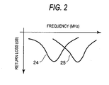
- Fig. 2 is an exemplary schematic diagram showing a receiving characteristic of the antenna switching system in Fig. 1.
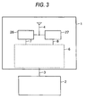
- Fig. 3 is an exemplary schematic diagram for explaining another embodiment of the antenna switching system shown in Fig. 1.
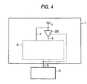
- Fig. 4 is an exemplary schematic diagram for explaining further another embodiment of the antenna switching system shown in Fig. 1.
- Fig. 5 is an exemplary schematic diagram for explaining further another embodiment of the antenna switching system shown in Fig. 1.
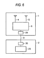
- Fig. 6 is an exemplary schematic diagram for explaining further another embodiment of the antenna switching system shown in Fig. 1.
- An antenna switching system (circuit module unit) according to a first embodiment includes an antenna unit 1, a receiving unit 2 and a feeder line 3 as shown in Fig. 1.
- the feeder line 3 is, for example, a coaxial cable, which connects the antenna unit 1 and the receiving unit 2 with each other.
- the antenna unit 1 includes: first and second antennas 4 and 5; and a switching circuit 6 for switching the antennas.
- the antennas 4 and 5 are provided for the following reason. That is, when a band to be received is, for example, a UHF band (470-770 MHz), it is difficult to obtain a desired characteristic only by a single antenna. Particularly, assume that an antenna is built in a small-sized mobile apparatus such as a cellular phone. Since the antenna is requested to be miniaturized, the miniaturized antenna cannot cover the whole band. It is therefore useful to switch two antennas by means of a switching circuit.
- a feed terminal 7 of the antenna 4 is connected to an input terminal 12(in) of an SPDT (Single Pole Double Throw) IC 12 through a DC-cutting capacitor 9.
- the SPDT IC 12 includes an FET (Field Effect Transistor).
- a feed terminal 8 of the antenna 5 is connected to the cathode side of a switching diode 11 and a resistor 22 through a DC-cutting capacitor 10. The other end of the resistor 22 is grounded.
- the anode side of the switching diode 11 is connected to an output terminal 13 of the SPDT IC 12 through a DC-cutting capacitor 16. The same anode side is also connected to a control terminal 14 of the SPDT IC 12 through a resistor 17. The other control terminal 15 of the SPDT IC is grounded.
- the receiving unit 2 has a receiving circuit 23.
- An input terminal 18 connected to the receiving circuit 23 through a DC-cutting capacitor 19 is connected to the feeder line 3 connected among the anode side of the switching diode 11, the DC-cutting capacitor 16 connected to the output terminal 13 of the SPDT IC 12, and the resistor 17.
- the receiving circuit 23 includes a control output terminal (output terminal) 21 capable of sending a control signal for switching the switching circuit 6.
- the receiving circuit 23 can perform switching control upon the SPDT IC 12 and the switching diode 11 (switch the both) in accordance with a control signal output from the output terminal 21.
- a characteristic 24 designates a return loss characteristic in view from the feed terminal 7 of the antenna 4
- a characteristic 25 designates a return loss characteristic in view from the feed terminal 8 of the antenna 5.
- the characteristic 24 corresponds to a frequency of a first frequency band of the whole receivable band
- the characteristic 25 corresponds to a frequency of a second frequency band at least a part of which does not overlap the first frequency band.
- the receiving circuit 23 Upon reception of a selection signal from the outside, the receiving circuit 23 acts as a unit for receiving the band of the characteristic 24. In this event, a control signal of "Low level (e.g. 0 V)" is output from the control output terminal 21. As a result, the control terminal 14 of the SPDT IC 12 is brought into “Low level” through the feeder line 3 so that the SPDT IC 12 is switched ON. Thus, electric continuity is established between the input and output (12 (in)-13) of the SPDT IC 12.
- Low level e.g. 0 V
- the control signal of "Low level” is also applied to the switching diode 11.
- the switching diode 11 is turned OFF, and released. That is, when the reception frequency is in the band of the characteristic 24, the SPDT IC 12 is turned ON and the switching diode 11 is turned OFF so that a reception signal input to the antenna 4 is sent to the receiving unit 2 without leaking to the antenna 5.
- the receiving circuit 23 Upon reception of a selection signal from the outside, the receiving circuit 23 acts as a unit for receiving the band of the characteristic 25. In this event, a control signal of "High level (e.g. 2.5 V)" is output from the control output terminal 21. As a result, the control terminal 14 of the SPDT IC 12 is brought into “High level” through the feeder line 3 so that the SPDT IC 12 is switched ON. Thus, electric discontinuity is established between the input and output (12 (in) -13) of the SPDT IC 12.
- High level e.g. 2.5 V
- the control signal of "High level” is also applied to the anode side of the switching diode 11 but the cathode side of the switching diode 11 is grounded through the resistor (high resistance) 22 so that the switching diode 11 is biased forward.
- a current flows into the switching diode 11 so that the switching diode 11 is turned ON, and electric continuity is established therein.
- the resistance value of the resistor 22 is 1 k ⁇ when the current flowing in the switching diode 11 is 1 mA. That is, when the reception frequency is in the band of the characteristic 25, the SPDT IC 12 is turned OFF and the switching diode 11 is turned ON so that a reception signal input to the antenna 5 is sent to the receiving unit 2 without leaking to the antenna 4.
- the DC-cutting capacitor 19 is inserted between the node 18 between the feeder line 3 and the control output terminal 21 and the receiving circuit 23, and an inductor 20 is inserted between the node 18 and the control output terminal 21 so that the reception signal is prevented from leaking to the control output terminal 21.
- the switching diode 11 is short of isolation in OFF time in comparison with the SPDT IC 12.
- a PIN diode may be used instead.
- attenuation in ON time increases so that the input sensitivity characteristic deteriorates.
- isolation in OFF time also increases so that leakage to the antenna 5 can be reduced more greatly.
- the SPDT IC 12 is replaced by a circuit consisting of an SPST (Single Pole Single Throw) IC or an FET.
- SPST Single Pole Single Throw
- An antenna unit 1 shown in Fig. 3 includes one antenna 4, first and second matching circuits 26 and 27, and a switching circuit 6.
- Each matching circuit 26, 27 includes, for example, an inductor and a capacitor.
- the matching circuits 26 and 27 give the antenna 4 a characteristic to allow the antenna 4 to receive the frequency of the first characteristic 24 of the predetermined band shown in Fig. 2 and a characteristic to allow the antenna 4 to receive the frequency of the second characteristic 25 of the same, respectively.
- the two matching circuits can be switched only by the feeder line 3. Not to say, there will be no problem if such a matching circuit is provided for only one of the antennas.
- An antenna unit 1 shown in Fig. 4 includes one antenna 4, a low noise switch 28 and a switching circuit 6.
- the antenna 4 is used for transmission and reception.
- the low noise amplifier 28 is required.
- the transmission level is reduced by passing through the low noise amplifier 28.
- the antenna 4 and a feed terminal 7 are connected as the transmitter side (TX), while the antenna 4 and a feed terminal 8 are connected through the low noise amplifier 28 as the receiver side (RX).
- switching can be made only by one feeder line 3 so that the feeder line 3 with the feed terminal 7 is turned ON (the feeder line 3 with the feed terminal 8 is turned OFF) at the time of transmission, and the feeder line 3 with the feed terminal 8 is turned ON (the feeder line 3 with the feed terminal 7 is turned OFF) at the time of reception.
- a control signal of "High level (e.g. 2.5 V)" is output from a control output terminal (21) at the time of reception. That is, the low noise amplifier 28 is turned ON (operable).
- a control signal of "Low level (e.g. 0 V)” is output so that the low noise amplifier 28 is turned OFF.
- Fig. 5 shows an antenna switching system according to a fourth embodiment.
- parts the same as those in Fig. 1 are referenced correspondingly, and description thereof will be simplified.
- An antenna unit 1 shown in Fig. 4 includes one antenna 4, first and second matching circuits 26 and 27, low noise amplifiers 31 and 32 connected to the matching circuits respectively, and a switching circuit 6.
- a band to be received is, for example, a UHF band (470-770 MHz)
- an antenna is built in a small-sized mobile apparatus such as a cellular phone.
- the antenna is requested to be miniaturized.
- a method for switching the first and second matching circuits 26 and 27 by a switch is useful to cover the whole band with one miniaturized antenna.
- the antenna 4 is used for transmission and reception. In order to gain sensitivity at the time of reception, the low noise amplifiers 31 and 32 are required. However, at the time of transmission, the transmission level is reduced due to the low noise amplifiers 31 and 32. Therefore, the antenna 4 and the switching circuit 6 are connected through a signal line 33 as the transmitter side (TX).
- the antenna 4 and a feed terminal 7 are connected through the first matching circuit 26 and the first low noise amplifier 31, and the antenna 4 and a feed terminal 8 are connected through a second matching circuit 27 and a second low noise amplifier 32.
- switching can be made only by one feeder line 3 so that the influence of the low noise amplifiers 31 and 32 can be eliminated at the time of transmission while the feeder line 3 with the feed terminal 7 is turned ON (the feeder line 3 with the feed terminal 8 is turned OFF) at the time of reception, and the feeder line 3 with the feed terminal 8 is turned ON (the feeder line 3 with the feed terminal 7 is turned OFF) at the time of reception.
- each low noise amplifier 31 and 32 is turned ON (operable) selectively correspondingly to each selected antenna 4, 5.
- the switch 34 may be changed over in sync with a selection signal supplied to the receiving circuit 23 from the outside.
- a communication signal serves as a jamming signal for the TV tuner whenever the cellular phone has communication.
- a cellular phone using a frequency band called a 800 MHz band is apt to suffer interfere because the frequency is very close to the frequency of a highest-frequency RF signal (770 MHz) of TV broadcasting waves, thereby causing degradation in TV image quality.
- signal processing circuits for eliminating jamming signals for example, filters (low pass filters, high pass filters, or band pass filters) or traps 29 and 30 having resonance points at jamming signal frequencies have to be provided on the lines of reception signals in the antenna unit 1 and the receiving unit 2.
- the transmission wave level of the cellular phone is up to +24 dBm and so high that filters or traps having attenuation of about 60 dB are required in consideration of isolation between the antenna of the TV tuner and the antenna of the cellular phone, the performance of the TV tuner, and so on.
- the circuit scale needs to be increased.
- the filters or traps are mounted on the tuner built in the cellular phone, they cannot be implemented by one chip, but at least two chips are required.
- the distance between input and output is so short that attenuation of the two chips theoretically expected to have a value 2 times as high as that of one chip decreases to about 1.7 times.
- the filters or traps 29 and 30 when the chips of the filters or traps 29 and 30 are disposed on the switching circuit 6 side and the receiving circuit 23 side respectively one by one through the feeder line 3, the filters or traps can be operated in cooperation with each other.
- the filters or traps 29 and 30 are not limited to chip forms. Similar effect can be obtained even if they are assemblies of a plurality of chip devices such as LCRs.
- the antenna switching system (circuit module unit) described above with reference to the embodiments is not limited to an appliance to a portable terminal, a cellular phone, a personal computer, a PC card, a high frequency module.
- the antenna switching system can be applied to any apparatus that is portable and provided with a TV tuner (TV receiving function) .
- an antenna switching system capable of switching signals received from two antennas having different characteristics for different bands respectively by use of a single feeder line so that the cost can be reduced and the space can be saved.
- circuit module unit capable of switching signals received from two antennas having different characteristics for different bands respectively by use of a single feeder line so that the cost can be reduced and the space can be saved.
- two chips of filters and traps for eliminating jamming signals are mounted on the antenna unit and the receiving unit respectively one by one, the jamming signals can be eliminated efficiently.
- the present invention is not limited to any one of the aforementioned embodiments. Various modifications or changes can be made on the invention without departing from the gist thereof when it is carried out.
- the embodiments may be combined with one another suitably if possible, or each embodiment may be partially deleted when it is carried out. On those occasions, various effects caused by the combination or deletion can be obtained.
Landscapes
- Engineering & Computer Science (AREA)
- Computer Networks & Wireless Communication (AREA)
- Signal Processing (AREA)
- Input Circuits Of Receivers And Coupling Of Receivers And Audio Equipment (AREA)
- Transceivers (AREA)
- Variable-Direction Aerials And Aerial Arrays (AREA)
Abstract
An antenna switching system includes: an antenna unit (1) having an antenna (4,5) and a switching circuit (6); a feeder line (3) connected to the switching circuit; and a receiving unit (2) connected to the feeder line. The switching circuit of the antenna unit is switched by a control signal supplied from a control signal sending portion included in the receiving unit.
Description
- This application is based upon and claims the benefit of priority from
Japanese Patent Application No. 2005-192984, filed on June 30, 2005 - One embodiment of the invention relates to a TV broadcasting receiving antenna switching system (circuit module unit) built in an apparatus such as a portable terminal, a cellular phone, a personal computer, a PC card, and a high frequency module.
- An apparatus, such as a portable terminal or a cellular phone, or such as a PC card or the like for use in a personal computer, having a capability of receiving TV broadcasting has been widely used.
- However, the frequency band used for TV broadcasting has a wide bandwidth due to its characteristic. It is therefore difficult to cover the whole bandwidth with a single antenna.
- In a portable terminal using radio waves in a frequency band close to a frequency band used for TV broadcasting, the radio waves used on the portable terminal might interfere with a TV tuner.
- There is disclosed, in
JP-A-7-297749 - The document
JP-A-7-297749 - According to the configuration disclosed in the document
JP-A-7-297749 - A general architecture that implements the various feature of the invention will now be described with reference to the drawings. The drawings and the associated descriptions are provided to illustrate embodiments of the invention and not to limit the scope of the invention.
- Fig. 1 is an exemplary schematic diagram for explaining an example of an antenna switching system according to an embodiment.
- Fig. 2 is an exemplary schematic diagram showing a receiving characteristic of the antenna switching system in Fig. 1.
- Fig. 3 is an exemplary schematic diagram for explaining another embodiment of the antenna switching system shown in Fig. 1.
- Fig. 4 is an exemplary schematic diagram for explaining further another embodiment of the antenna switching system shown in Fig. 1.
- Fig. 5 is an exemplary schematic diagram for explaining further another embodiment of the antenna switching system shown in Fig. 1.
- Fig. 6 is an exemplary schematic diagram for explaining further another embodiment of the antenna switching system shown in Fig. 1.
- Embodiments according to the invention will be described hereinafter with reference to the accompanying drawings.
- An antenna switching system (circuit module unit) according to a first embodiment includes an
antenna unit 1, areceiving unit 2 and afeeder line 3 as shown in Fig. 1. Thefeeder line 3 is, for example, a coaxial cable, which connects theantenna unit 1 and thereceiving unit 2 with each other. - The
antenna unit 1 includes: first andsecond antennas switching circuit 6 for switching the antennas. Theantennas - A
feed terminal 7 of theantenna 4 is connected to an input terminal 12(in) of an SPDT (Single Pole Double Throw) IC 12 through a DC-cutting capacitor 9. For example, the SPDT IC 12 includes an FET (Field Effect Transistor). - A
feed terminal 8 of theantenna 5 is connected to the cathode side of aswitching diode 11 and aresistor 22 through a DC-cutting capacitor 10. The other end of theresistor 22 is grounded. - The anode side of the
switching diode 11 is connected to anoutput terminal 13 of the SPDT IC 12 through a DC-cutting capacitor 16. The same anode side is also connected to acontrol terminal 14 of the SPDT IC 12 through aresistor 17. Theother control terminal 15 of the SPDT IC is grounded. - The
receiving unit 2 has areceiving circuit 23. Aninput terminal 18 connected to thereceiving circuit 23 through a DC-cutting capacitor 19 is connected to thefeeder line 3 connected among the anode side of theswitching diode 11, the DC-cutting capacitor 16 connected to theoutput terminal 13 of the SPDTIC 12, and theresistor 17. - The
receiving circuit 23 includes a control output terminal (output terminal) 21 capable of sending a control signal for switching theswitching circuit 6. Thereceiving circuit 23 can perform switching control upon the SPDT IC 12 and the switching diode 11 (switch the both) in accordance with a control signal output from theoutput terminal 21. - In the SPDT IC 12, electric continuity is established between input and output (12(in)-13) when the two
control terminals control terminal 14 is in "High level" and thecontrol terminal 15 is in "Low level". - Next, the operation of the embodiment of the invention will be described in detail with reference to Figs. 1 and 2. In Fig. 2, a
characteristic 24 designates a return loss characteristic in view from thefeed terminal 7 of theantenna 4, and acharacteristic 25 designates a return loss characteristic in view from thefeed terminal 8 of theantenna 5. Not to say, thecharacteristic 24 corresponds to a frequency of a first frequency band of the whole receivable band, and thecharacteristic 25 corresponds to a frequency of a second frequency band at least a part of which does not overlap the first frequency band. - First, description will be made about the operation when the reception frequency is in the band of the characteristic 24.
- Upon reception of a selection signal from the outside, the
receiving circuit 23 acts as a unit for receiving the band of the characteristic 24. In this event, a control signal of "Low level (e.g. 0 V)" is output from thecontrol output terminal 21. As a result, thecontrol terminal 14 of the SPDT IC 12 is brought into "Low level" through thefeeder line 3 so that the SPDT IC 12 is switched ON. Thus, electric continuity is established between the input and output (12 (in)-13) of the SPDTIC 12. - In this case, the control signal of "Low level" is also applied to the
switching diode 11. However, no current flows into theswitching diode 11. Thus, theswitching diode 11 is turned OFF, and released. That is, when the reception frequency is in the band of the characteristic 24, the SPDTIC 12 is turned ON and theswitching diode 11 is turned OFF so that a reception signal input to theantenna 4 is sent to thereceiving unit 2 without leaking to theantenna 5. - Next, description will be made about the operation where the reception frequency is in the band of the characteristic 25.
- Upon reception of a selection signal from the outside, the
receiving circuit 23 acts as a unit for receiving the band of the characteristic 25. In this event, a control signal of "High level (e.g. 2.5 V)" is output from thecontrol output terminal 21. As a result, thecontrol terminal 14 of the SPDT IC 12 is brought into "High level" through thefeeder line 3 so that the SPDT IC 12 is switched ON. Thus, electric discontinuity is established between the input and output (12 (in) -13) of theSPDT IC 12. - In this case, the control signal of "High level" is also applied to the anode side of the
switching diode 11 but the cathode side of theswitching diode 11 is grounded through the resistor (high resistance) 22 so that theswitching diode 11 is biased forward. Thus, a current flows into theswitching diode 11 so that theswitching diode 11 is turned ON, and electric continuity is established therein. For example, the resistance value of theresistor 22 is 1 kΩ when the current flowing in theswitching diode 11 is 1 mA. That is, when the reception frequency is in the band of the characteristic 25, theSPDT IC 12 is turned OFF and the switchingdiode 11 is turned ON so that a reception signal input to theantenna 5 is sent to the receivingunit 2 without leaking to theantenna 4. - The DC-cutting
capacitor 19 is inserted between thenode 18 between thefeeder line 3 and thecontrol output terminal 21 and the receivingcircuit 23, and aninductor 20 is inserted between thenode 18 and thecontrol output terminal 21 so that the reception signal is prevented from leaking to thecontrol output terminal 21. - The switching
diode 11 is short of isolation in OFF time in comparison with theSPDT IC 12. For example, a PIN diode may be used instead. When a PIN diode is used, attenuation in ON time increases so that the input sensitivity characteristic deteriorates. However, isolation in OFF time also increases so that leakage to theantenna 5 can be reduced more greatly. - In case where a function similar to the aforementioned function can be obtained, there will be no problem that the
SPDT IC 12 is replaced by a circuit consisting of an SPST (Single Pole Single Throw) IC or an FET. - Next, an antenna switching system according to a second embodiment will be described with reference to Fig. 3. In Fig. 3, parts the same as those in Fig. 1 are referenced correspondingly, and description thereof will be simplified.
- An
antenna unit 1 shown in Fig. 3 includes oneantenna 4, first andsecond matching circuits switching circuit 6. - When a band to be received is, for example, a UHF band (470-770 MHz), it is difficult to obtain a desired characteristic only by a single antenna. In a case where an antenna is built in a small-sized mobile apparatus such as a cellular phone, the antenna is required to be miniaturized. To this end, a method for switching the first and
second matching circuits circuit circuits antenna 4 to receive the frequency of the first characteristic 24 of the predetermined band shown in Fig. 2 and a characteristic to allow theantenna 4 to receive the frequency of the second characteristic 25 of the same, respectively. - In this case, when the
switching circuit 6 described in the embodiment shown in Fig. 1 is used, the two matching circuits can be switched only by thefeeder line 3. Not to say, there will be no problem if such a matching circuit is provided for only one of the antennas. - Next, an antenna switching system according to a third embodiment will be described with reference to Fig. 4. In Fig. 4, parts the same as those in Fig. 1 are referenced correspondingly, and description thereof will be simplified.
- An
antenna unit 1 shown in Fig. 4 includes oneantenna 4, alow noise switch 28 and aswitching circuit 6. - The
antenna 4 is used for transmission and reception. In order to gain sensitivity at the time of reception, thelow noise amplifier 28 is required. However, at the time of transmission, there is a problem that the transmission level is reduced by passing through thelow noise amplifier 28. - As shown in Fig. 4, the
antenna 4 and afeed terminal 7 are connected as the transmitter side (TX), while theantenna 4 and afeed terminal 8 are connected through thelow noise amplifier 28 as the receiver side (RX). By use of theswitching circuit 6 described with reference to Fig. 1, switching can be made only by onefeeder line 3 so that thefeeder line 3 with thefeed terminal 7 is turned ON (thefeeder line 3 with thefeed terminal 8 is turned OFF) at the time of transmission, and thefeeder line 3 with thefeed terminal 8 is turned ON (thefeeder line 3 with thefeed terminal 7 is turned OFF) at the time of reception. - It is necessary to supply power to the
low noise amplifier 28. When thefeeder line 3 and a power terminal of thelow noise amplifier 28 are connected, a control signal of "High level (e.g. 2.5 V)" is output from a control output terminal (21) at the time of reception. That is, thelow noise amplifier 28 is turned ON (operable). On the other hand, at the time of transmission, a control signal of "Low level (e.g. 0 V)" is output so that thelow noise amplifier 28 is turned OFF. Thus, excessive power consumption can be suppressed at the time of transmission (power consumption can be suppressed) . In addition, according to this method, influence of the low noise amplifier 28 (reduction in transmission level) can be prevented at the time of transmission. - Fig. 5 shows an antenna switching system according to a fourth embodiment. In Fig. 5, parts the same as those in Fig. 1 are referenced correspondingly, and description thereof will be simplified.
- An
antenna unit 1 shown in Fig. 4 includes oneantenna 4, first andsecond matching circuits low noise amplifiers switching circuit 6. When a band to be received is, for example, a UHF band (470-770 MHz), it is difficult to obtain a desired characteristic only by a single antenna as described with reference to Fig. 1. Particularly, assume that an antenna is built in a small-sized mobile apparatus such as a cellular phone. In this case, the antenna is requested to be miniaturized. To this end, a method for switching the first andsecond matching circuits - The
antenna 4 is used for transmission and reception. In order to gain sensitivity at the time of reception, thelow noise amplifiers low noise amplifiers antenna 4 and theswitching circuit 6 are connected through asignal line 33 as the transmitter side (TX). - On the other hand, as the receiver side (RX), the
antenna 4 and afeed terminal 7 are connected through thefirst matching circuit 26 and the firstlow noise amplifier 31, and theantenna 4 and afeed terminal 8 are connected through asecond matching circuit 27 and a secondlow noise amplifier 32. - Thus, by use of the
switching circuit 6 described in Fig. 1, switching can be made only by onefeeder line 3 so that the influence of thelow noise amplifiers feeder line 3 with thefeed terminal 7 is turned ON (thefeeder line 3 with thefeed terminal 8 is turned OFF) at the time of reception, and thefeeder line 3 with thefeed terminal 8 is turned ON (thefeeder line 3 with thefeed terminal 7 is turned OFF) at the time of reception. - It is necessary to supply power to the
low noise amplifiers supply changeover switch 34 between thefeeder line 3 and eachlow noise amplifier low noise amplifier antenna switch 34 may be changed over in sync with a selection signal supplied to the receivingcircuit 23 from the outside. - In the embodiment described above, when the aforementioned circuit is built in a small-sized mobile apparatus such as a cellular phone, switching between two antennas, between two matching circuits and between transmission and reception can be controlled by only one feeder line. Thus, the layout can be arranged easily, and the space and the cost can be saved.
- Next, an antenna switching system according to a fifth embodiment will be described with reference to Fig. 6. In Fig. 6, parts the same as those in Fig. 1 are referenced correspondingly, and description thereof will be simplified.
- When a TV tuner is built in a cellular phone, the cellular phone frequently communicates with a base station regardless of whether it has a call or not. Accordingly, a communication signal serves as a jamming signal for the TV tuner whenever the cellular phone has communication.
- For example, a cellular phone using a frequency band called a 800 MHz band is apt to suffer interfere because the frequency is very close to the frequency of a highest-frequency RF signal (770 MHz) of TV broadcasting waves, thereby causing degradation in TV image quality.
- Therefore, signal processing circuits for eliminating jamming signals, for example, filters (low pass filters, high pass filters, or band pass filters) or traps 29 and 30 having resonance points at jamming signal frequencies have to be provided on the lines of reception signals in the
antenna unit 1 and the receivingunit 2. - However, the transmission wave level of the cellular phone is up to +24 dBm and so high that filters or traps having attenuation of about 60 dB are required in consideration of isolation between the antenna of the TV tuner and the antenna of the cellular phone, the performance of the TV tuner, and so on.
- In order to attain such high attenuation, however, the circuit scale needs to be increased. In addition, when the filters or traps are mounted on the tuner built in the cellular phone, they cannot be implemented by one chip, but at least two chips are required.
- When the two chips are mounted on the
antenna unit 1 or thereception unit 2, the distance between input and output is so short that attenuation of the two chips theoretically expected to have avalue 2 times as high as that of one chip decreases to about 1.7 times. - When the filters or traps 29 and 30 are provided on the
antenna unit 1 and the receivingunit 2 respectively one by one, it is possible to obtain attenuation of about 2 times. - That is, when the chips of the filters or traps 29 and 30 are disposed on the
switching circuit 6 side and the receivingcircuit 23 side respectively one by one through thefeeder line 3, the filters or traps can be operated in cooperation with each other. - The filters or traps 29 and 30 are not limited to chip forms. Similar effect can be obtained even if they are assemblies of a plurality of chip devices such as LCRs.
- The antenna switching system (circuit module unit) described above with reference to the embodiments is not limited to an appliance to a portable terminal, a cellular phone, a personal computer, a PC card, a high frequency module. The antenna switching system can be applied to any apparatus that is portable and provided with a TV tuner (TV receiving function) .
- According to the present invention, there is provided an antenna switching system (circuit module unit) capable of switching signals received from two antennas having different characteristics for different bands respectively by use of a single feeder line so that the cost can be reduced and the space can be saved. In addition, when two chips of filters and traps for eliminating jamming signals are mounted on the antenna unit and the receiving unit respectively one by one, the jamming signals can be eliminated efficiently.
- The present invention is not limited to any one of the aforementioned embodiments. Various modifications or changes can be made on the invention without departing from the gist thereof when it is carried out. The embodiments may be combined with one another suitably if possible, or each embodiment may be partially deleted when it is carried out. On those occasions, various effects caused by the combination or deletion can be obtained.
- It is to be understood that the invention is not limited to the specific embodiments described above and that the invention can be embodied with the components modified without departing from the spirit and scope of the invention. The invention can be embodied in various forms according to appropriate combinations of the components disclosed in the embodiment described above. For example, some components may be deleted from all components shown in the embodiment. Further, the components in different embodiments may be used appropriately in combination.
Claims (7)
- An antenna switching system comprising:an antenna unit;a receiving unit; anda single feeder line that connects the antenna unit and the receiving unit,wherein the antenna unit comprises:an antenna that receives a first signal of a first frequency band and a second signal of a second frequency band; anda switching circuit that is connected to the antenna and the feeder line, and selectively outputs one of the first signal and the second signal, andwherein the receiving unit supplies a switching signal to the switching circuit through the feeder line and selectively receives one of the first and second signals through the feeder line, the switching signal controlling the output by the switching circuit.
- The antenna switching system according to claim 1, wherein the switching circuit comprises:a signal processing unit that is connected to the antenna and the feeder line, and receives from the antenna the first signal of the first frequency band;a unidirectional device that is connected to the antenna and the feeder line, and receives from the antenna the second signal of the second frequency band; anda bias resistor that biases the unidirectional device.
- The antenna switching system according to claim 1, wherein the antenna comprises:a first antenna that has a reception characteristic in the first frequency band; anda second antenna that has a reception characteristic in the second frequency band that partially overlaps with the first frequency band,wherein the signal processing unit is connected to the first antenna, and
wherein the unidirectional device is connected to the second antenna. - The antenna switching system according to claim 1, wherein the antenna has a reception characteristic of a third frequency band that includes the first frequency band and the second frequency band,
wherein the antenna unit further comprises:a first matching circuit that allows the antenna to receive the first signal of the first frequency band; anda second matching circuit that allows the antenna to receive the second signal of the second frequency band, at least a part of the second frequency band being set to unoverlap with the first frequency band. - The antenna switching system according to claim 1, wherein the antenna comprises:a first antenna that has a reception characteristic in the first frequency band; anda second antenna that has a reception characteristic in the second frequency band that partially overlaps with the first frequency band,wherein the antenna unit further comprises a first signal processing circuit that reduces components having influence on the signal to be received by the receiving unit, and
wherein the receiving unit further comprises a second signal processing circuit that reduces components having influence on the signal to be received by the receiving unit in cooperation with the first signal processing circuit. - An antenna switching system comprising:an antenna unit;a receiving unit; anda single feeder line that connects the antenna unit and the receiving unit,wherein the antenna unit comprises:an antenna that receives a reception signal of a predetermined frequency band;an amplifier that amplifies the reception signal received by the antenna;a switching circuit that is connected to the antenna and the feeder line, and selectively performs one of outputting the reception signal amplified by the amplifier to the receiving unit through the feeder line, and outputting a transmission signal input through the feeder line to the antenna, andwherein the receiving unit supplies a switching signal to the switching circuit through the feeder line, the switching signal controlling the selection by the switching circuit and supplying power to the amplifier.
- The antenna switching system according to claim 6, wherein the antenna has a reception characteristic of a third frequency band that includes the first frequency band and the second frequency band,
wherein the antenna unit further comprises:a first matching circuit that allows the antenna to receive the first signal of the first frequency band; anda second matching circuit that allows the antenna to receive the second signal of the second frequency band, at least a part of the second frequency band being set to unoverlap with the first frequency band,wherein the amplifier comprises:a first amplifier that amplifies the first signal; anda second amplifier that amplifies the second signal, andwherein the receiving unit supplies the switching signal that supplies power to one of the first amplifier and the second amplifier.
Applications Claiming Priority (1)
| Application Number | Priority Date | Filing Date | Title |
|---|---|---|---|
| JP2005192984A JP2007013715A (en) | 2005-06-30 | 2005-06-30 | Antenna switch system |
Publications (1)
| Publication Number | Publication Date |
|---|---|
| EP1739857A2 true EP1739857A2 (en) | 2007-01-03 |
Family
ID=37052591
Family Applications (1)
| Application Number | Title | Priority Date | Filing Date |
|---|---|---|---|
| EP06116249A Pending EP1739857A2 (en) | 2005-06-30 | 2006-06-28 | Antenna switching system |
Country Status (3)
| Country | Link |
|---|---|
| US (1) | US20070004345A1 (en) |
| EP (1) | EP1739857A2 (en) |
| JP (1) | JP2007013715A (en) |
Cited By (1)
| Publication number | Priority date | Publication date | Assignee | Title |
|---|---|---|---|---|
| RU226570U1 (en) * | 2024-04-16 | 2024-06-11 | Акционерное общество "Информтехника и Связь" (АО "Информтехника и Связь") | Alarm system switching device |
Families Citing this family (8)
| Publication number | Priority date | Publication date | Assignee | Title |
|---|---|---|---|---|
| TWI352450B (en) * | 2007-12-12 | 2011-11-11 | Wistron Neweb Corp | Transceiver device of wireless signals and related |
| JP2010252161A (en) * | 2009-04-17 | 2010-11-04 | Hitachi Kokusai Electric Inc | Diode switch circuit |
| WO2011118020A1 (en) * | 2010-03-26 | 2011-09-29 | パイオニア株式会社 | Receiving apparatus |
| EP2813121A2 (en) * | 2012-01-11 | 2014-12-17 | Interdigital Patent Holdings, Inc. | Adaptive control channel |
| JP5974944B2 (en) * | 2013-03-21 | 2016-08-23 | ソニー株式会社 | Mobile device |
| US9885787B2 (en) * | 2014-07-28 | 2018-02-06 | Echostar Technologies L.L.C. | Electronic satellite feed switcher |
| WO2020033160A1 (en) | 2018-08-08 | 2020-02-13 | Avx Antenna, Inc. D/B/A Ethertronics, Inc. | Methods for configuring a multi-mode antenna system for multi-channel communication systems |
| WO2020033158A1 (en) * | 2018-08-08 | 2020-02-13 | Avx Antenna, Inc. D/B/A Ethertronics, Inc. | Vhf-uhf antenna system with feedback |
-
2005
- 2005-06-30 JP JP2005192984A patent/JP2007013715A/en not_active Withdrawn
-
2006
- 2006-06-28 EP EP06116249A patent/EP1739857A2/en active Pending
- 2006-06-28 US US11/475,981 patent/US20070004345A1/en not_active Abandoned
Cited By (1)
| Publication number | Priority date | Publication date | Assignee | Title |
|---|---|---|---|---|
| RU226570U1 (en) * | 2024-04-16 | 2024-06-11 | Акционерное общество "Информтехника и Связь" (АО "Информтехника и Связь") | Alarm system switching device |
Also Published As
| Publication number | Publication date |
|---|---|
| JP2007013715A (en) | 2007-01-18 |
| US20070004345A1 (en) | 2007-01-04 |
Similar Documents
| Publication | Publication Date | Title |
|---|---|---|
| US8774067B2 (en) | Antenna impedance stabilization with stabilization load in second antenna circuitry | |
| US7511681B2 (en) | Switchable antenna arrangement | |
| KR100698971B1 (en) | Dual band radiotelephone with receiving and transmitting antenna and related method | |
| AU724641B2 (en) | Dual-band antenna coupler for a portable radiotelephone | |
| KR100989064B1 (en) | Multiple resonant antenna | |
| US6154177A (en) | Antenna device and radio receiver using the same | |
| US6653697B2 (en) | High frequency switch circuit and communications terminal using the same | |
| US20120050122A1 (en) | Antenna module and impedance matching method thereof | |
| US6510310B1 (en) | Dual mode phone architecture utilizing a single transmit-receive switch | |
| US20060229035A1 (en) | High-frequency circuit and communications apparatus comprising same | |
| KR20010043766A (en) | Harmonic suppression in dual band mobile phones | |
| US7340274B2 (en) | Cellular phone capable of receiving a plurality of broadcast waves | |
| US20060009164A1 (en) | Radio frequency switching circuit | |
| US20160126640A1 (en) | Diversity antenna apparatus of mobile terminal and implementation method thereof | |
| US12348192B2 (en) | Radio-frequency amplifier circuitry with improved transmit and receive performance | |
| US20070004345A1 (en) | Antenna switching system | |
| EP2134000B1 (en) | Multi-band mobile communication device | |
| US6718157B1 (en) | Apparatus for commonly using antenna for call signal and television broadcasting signal in radio communication terminal | |
| US9819077B1 (en) | Multi-feed antenna optimized for non-50 Ohm operation | |
| EP1916774A1 (en) | Antenna device and portable radio communication device comprising such antenna device | |
| US7602346B2 (en) | Antenna module, radio device and mobile radio terminal | |
| US8665171B2 (en) | Diversity antenna apparatus including rectifier device | |
| US20230223690A1 (en) | Antenna module and communication device incorporating the same | |
| US11949437B2 (en) | Wideband antenna system | |
| KR100318916B1 (en) | Power amplifier controling apparatus of multi-band frequency processing radio terminal |
Legal Events
| Date | Code | Title | Description |
|---|---|---|---|
| PUAI | Public reference made under article 153(3) epc to a published international application that has entered the european phase |
Free format text: ORIGINAL CODE: 0009012 |
|
| AK | Designated contracting states |
Kind code of ref document: A2 Designated state(s): AT BE BG CH CY CZ DE DK EE ES FI FR GB GR HU IE IS IT LI LT LU LV MC NL PL PT RO SE SI SK TR |
|
| AX | Request for extension of the european patent |
Extension state: AL BA HR MK YU |
|
| STAA | Information on the status of an ep patent application or granted ep patent |
Free format text: STATUS: THE APPLICATION HAS BEEN WITHDRAWN |
|
| 18W | Application withdrawn |
Effective date: 20090226 |
|
| D18W | Application withdrawn (deleted) | ||
| R18W | Application withdrawn (corrected) |
Effective date: 20090226 |