EP1739846A2 - Signal generating apparatus, IC chip, GPS receiver, and cellular phone - Google Patents
Signal generating apparatus, IC chip, GPS receiver, and cellular phone Download PDFInfo
- Publication number
- EP1739846A2 EP1739846A2 EP06010288A EP06010288A EP1739846A2 EP 1739846 A2 EP1739846 A2 EP 1739846A2 EP 06010288 A EP06010288 A EP 06010288A EP 06010288 A EP06010288 A EP 06010288A EP 1739846 A2 EP1739846 A2 EP 1739846A2
- Authority
- EP
- European Patent Office
- Prior art keywords
- frequency
- signal
- composition purpose
- purpose signal
- composition
- Prior art date
- Legal status (The legal status is an assumption and is not a legal conclusion. Google has not performed a legal analysis and makes no representation as to the accuracy of the status listed.)
- Withdrawn
Links
- 230000001413 cellular effect Effects 0.000 title claims description 32
- 239000000203 mixture Substances 0.000 claims abstract description 61
- 239000002131 composite material Substances 0.000 claims abstract description 16
- 238000010897 surface acoustic wave method Methods 0.000 description 14
- 230000035945 sensitivity Effects 0.000 description 10
- 238000000034 method Methods 0.000 description 9
- 230000007423 decrease Effects 0.000 description 7
- 230000005540 biological transmission Effects 0.000 description 5
- 230000008901 benefit Effects 0.000 description 3
- 238000006243 chemical reaction Methods 0.000 description 3
- 230000009467 reduction Effects 0.000 description 3
- 230000008859 change Effects 0.000 description 2
- 239000013078 crystal Substances 0.000 description 2
- 230000008569 process Effects 0.000 description 2
- 230000001629 suppression Effects 0.000 description 2
- 230000003247 decreasing effect Effects 0.000 description 1
- 230000008030 elimination Effects 0.000 description 1
- 238000003379 elimination reaction Methods 0.000 description 1
- 230000006870 function Effects 0.000 description 1
- 230000010355 oscillation Effects 0.000 description 1
- 230000002265 prevention Effects 0.000 description 1
Images



Classifications
-
- H—ELECTRICITY
- H03—ELECTRONIC CIRCUITRY
- H03L—AUTOMATIC CONTROL, STARTING, SYNCHRONISATION OR STABILISATION OF GENERATORS OF ELECTRONIC OSCILLATIONS OR PULSES
- H03L7/00—Automatic control of frequency or phase; Synchronisation
- H03L7/06—Automatic control of frequency or phase; Synchronisation using a reference signal applied to a frequency- or phase-locked loop
- H03L7/16—Indirect frequency synthesis, i.e. generating a desired one of a number of predetermined frequencies using a frequency- or phase-locked loop
- H03L7/18—Indirect frequency synthesis, i.e. generating a desired one of a number of predetermined frequencies using a frequency- or phase-locked loop using a frequency divider or counter in the loop
-
- G—PHYSICS
- G01—MEASURING; TESTING
- G01S—RADIO DIRECTION-FINDING; RADIO NAVIGATION; DETERMINING DISTANCE OR VELOCITY BY USE OF RADIO WAVES; LOCATING OR PRESENCE-DETECTING BY USE OF THE REFLECTION OR RERADIATION OF RADIO WAVES; ANALOGOUS ARRANGEMENTS USING OTHER WAVES
- G01S19/00—Satellite radio beacon positioning systems; Determining position, velocity or attitude using signals transmitted by such systems
- G01S19/01—Satellite radio beacon positioning systems transmitting time-stamped messages, e.g. GPS [Global Positioning System], GLONASS [Global Orbiting Navigation Satellite System] or GALILEO
- G01S19/13—Receivers
-
- H—ELECTRICITY
- H04—ELECTRIC COMMUNICATION TECHNIQUE
- H04B—TRANSMISSION
- H04B1/00—Details of transmission systems, not covered by a single one of groups H04B3/00 - H04B13/00; Details of transmission systems not characterised by the medium used for transmission
- H04B1/38—Transceivers, i.e. devices in which transmitter and receiver form a structural unit and in which at least one part is used for functions of transmitting and receiving
- H04B1/3805—Transceivers, i.e. devices in which transmitter and receiver form a structural unit and in which at least one part is used for functions of transmitting and receiving with built-in auxiliary receivers
-
- H—ELECTRICITY
- H04—ELECTRIC COMMUNICATION TECHNIQUE
- H04B—TRANSMISSION
- H04B15/00—Suppression or limitation of noise or interference
- H04B15/02—Reducing interference from electric apparatus by means located at or near the interfering apparatus
- H04B15/04—Reducing interference from electric apparatus by means located at or near the interfering apparatus the interference being caused by substantially sinusoidal oscillations, e.g. in a receiver or in a tape-recorder
- H04B15/06—Reducing interference from electric apparatus by means located at or near the interfering apparatus the interference being caused by substantially sinusoidal oscillations, e.g. in a receiver or in a tape-recorder by local oscillators of receivers
-
- H—ELECTRICITY
- H03—ELECTRONIC CIRCUITRY
- H03J—TUNING RESONANT CIRCUITS; SELECTING RESONANT CIRCUITS
- H03J2200/00—Indexing scheme relating to tuning resonant circuits and selecting resonant circuits
- H03J2200/11—Cellular receiver, e.g. GSM, combined with a GPS receiver
Definitions
- the present invention relates to a receiver which receives signals for positioning.
- GPS Global Positioning System
- PDA Personal Digital Assistants
- a communication signal transmitted from the cellular phone or the like may be an interference wave to GPS signals to be received by the GPS receiver.
- conventional GPS receivers have allowed simultaneous use of a GPS receiver and a cellular phone or a PDA by eliminating a communication signal transmitted from the cellular phone or the like from a receiving signal using a SAW (SurfaceAcoustic Wave)filter(e.g., JP-A-2003-255036 [0043]).
- SAW SurfaceAcoustic Wave
- filters such as the SAW filter and the like allow elimination of communication signals which are interference waves, but causes decrease in the S/N ratio (Signal to Noise ratio) of several dBm of GPS signals. Accordingly, there is a problem that the above-mentioned conventional GPS receivers may not obtain high sensitivity in terms of GPS signals when the GPS receiver and a cellular phone or the like are being used simultaneously.
- an advantage of some aspects of the invention is to provide a composition purpose signal generating apparatus, an IC (Integrated Circuit) chip, a GPS receiver, and a cellular phone, which allow obtainment of high sensitivity in terms of receiving signals without being affected by interference waves without using a filter such as a SAW filter or the like, when reception/ transmission of communication signals and reception of positioning signals are carried out simultaneously.
- a composition purpose signal generating apparatus an IC (Integrated Circuit) chip, a GPS receiver, and a cellular phone
- a composition purpose signal generating apparatus which includes an oscillator for outputting a composition purpose signal to a frequency changing apparatus which outputs a composite wave consisting of a receiving signal and the composition purpose signal as an intermediate frequency signal, a frequency divider for dividing the frequency of the composition purpose signal output from the oscillator, a reference oscillator for outputting a reference signal, a phase comparator for outputting phase difference data which indicates a phase difference between the composition purpose signal which is frequency divided by the frequency divider and the reference signal, and a filter for outputting the phase difference data output from the phase comparator as a control voltage of the oscillator, includes composition purpose signal frequency changing means for changing the frequency of the composition purpose signal when the frequency of a composite wave consisting of a basic wave or harmonic constituting a communication signal which is interference wave to the receiving signal and a basic wave or harmonic constituting the composition purpose signal is almost equal to the frequency of the intermediate frequency signal.
- the receiving signal and the composition purpose signal are compounded as well as a basic wave or harmonic constituting a communication signal which is an interference wave to the receiving signal and a basic wave or harmonic constituting the composition purpose signal are compounded. Accordingly, even if the frequency of the communication signal is different from that of the receiving signal, the frequency of the composite wave consisting of a basic wave or harmonic constituting the communication signal and a basic wave or harmonic constituting the composition purpose signal may be almost equal to the frequency of the intermediate frequency signal. In this case, the intermediate frequency signal which is a composite wave consisting of the receiving signal and the composition purpose signal and a composite wave consisting of the communication signal and the composition purpose signal cannot be identified, resulting in decrease in the sensitivity of the receiver.
- the composition purpose signal generating apparatus can change the frequency of the composition purpose signal using the composition purpose signal frequency changing means when the frequency of the composite wave consisting of a basic wave or harmonic constituting the communication signal which is an interference wave to the receiving signal and a basic wave or harmonic constituting the composition purpose signal is almost equal to the frequency of the intermediate frequency signal.
- a second aspect of the invention is a composition purpose signal generating apparatus with a structure according to the first aspect of the invention, includes a plurality of frequency dividers with different frequency dividing ratios, wherein the composition purpose signal changing means changes the frequency of the composition purpose signal by switching the frequency divider to another one with different frequency dividing ratio.
- the composition purpose signal frequency changing means switches the frequency divider to another one with different frequency dividing ratio.
- the control voltage generated by the phase comparator can be switched by switching the frequency divider, allowing switching of the frequency of the composition purpose signal output from the oscillator.
- a third aspect of the invention is a composition purpose signal generating apparatus with a structure according to the first aspect of the invention, includes a.plurality of reference oscillators which outputs different frequencies, wherein the composition purpose signal changing means changes the frequency of the composition purpose signal by switching the reference oscillator to another one which outputs different frequency.
- the composition purpose signal frequency changing means switches the reference oscillator to another one which outputs different frequency.
- the control voltage generated by the phase comparator can be switched by switching the reference oscillator, allowing switching of the frequency of the composition purpose signal output from the oscillator.
- an IC chip includes the composition purpose signal generating apparatus according to any of the first through the third aspect of the invention.
- the IC chip can suppress the influence of the interference wave without using the SAW filter, allowing reduction in the size of the receiver.
- a GPS receiver includes the IC chip according to fourth aspect of the invention.
- a cellular phone includes the IC chip according to fourth aspect of the invention.
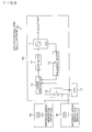
- Fig. 1 shows a GPS locator-equipped cellular phone in an embodiment according to the invention.
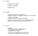
- Fig. 2 shows an example of GPS signal and the like.
- Fig. 3 shows an exemplary structure of a PLL device.
- Fig. 4 shows a flowchart of an operation example of the GPS locator-equipped cellular phone 1.
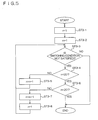
- Fig. 5 shows a flowchart of an operation example of the GPS locator-equipped cellular phone 1.
- Fig. 6 shows an exemplary structure of a PLL device.
- Fig. 1 schematically illustrates a GPS locator-equipped cellular phone 1 according to a first embodiment of the invention.
- the GPS locator-equipped cellular phone 1 includes a GPS receiving section 2 for receiving a GPS signal S (see Fig. 2 A), and a communication section 3 for receiving/ transmitting a communication signal CS (see Fig. 2 B).
- the GPS signal S is an example of receiving signals.
- the communication signal CS is an interference wave to the GPS signal S, to be described later.
- the GPS locator-equipped cellular phone 1 includes the GPS receiving section 2.
- the GPS receiving section 2 includes a CPU 10 for controlling each section, an antenna 4 for receiving the GPS signal, and the like.
- the GPS receiving section 2 also includes a reference signal generating apparatus 9 for outputting a reference signal.
- the reference signal generating apparatus 9 may be a crystal oscillator, for example, which can stably generate predetermined frequencies.
- the reference signal generating apparatus 9 is an example of reference oscillators.
- the GPS receiving section 2 also includes amplifiers 5 and 7, a down converting apparatus 6, and a PLL (Phase Locked Loop) device 8.
- PLL Phase Locked Loop
- the down converting apparatus 6 outputs a composite wave consisting of the GPS signal S received by the antenna 4 and input through the amplifier 5 and the LO signal output from the PLL device 8 as an IF (Intermediate Frequency) signal.
- the LO signal is an example of composition purpose signals.
- the PLL device 8, the reference signal generating apparatus 9, and the CPU 10 are an example of the composition purpose signal generating apparatus.
- the IF signal is an example of the intermediate frequency signals.
- the down converting apparatus 6 is an example of frequency converting apparatus.
- Fig. 2 illustrates an example of frequencies and the like of the GPS signal S to be received by the antenna 4.
- the GPS signal S of 1575.42 MHz and the LO signal of 1575.288 MHz are multiplied on a circuit basis in the down converting apparatus 6 (see Fig. 1), generating the IF signal of 132 kHz.
- the frequency of quadruple wave thereof is 7876.308 MHz.
- the frequency of quintuple wave of the LO signal of 1575.288 MHz is 7876.44 MHz.
- the quadruple wave of the communication signal CS and the quintuple wave of the LO signal are multiplied on a circuit basis in the down converting apparatus 6, generating a signal of 132 kHz.
- the communication signal CS is an interference wave to the GPS signal S.
- the following structure of the GPS locator-equipped cellular phone 1 can prevent the communication signal CS from being an interference wave to the GPS signal S.
- Fig. 3 schematically illustrates an example of a structure of the PLL device 8 and the like.
- the PLL device 8 includes a VCO (Voltage Controlled Oscillator) 11.
- the VCO 11 outputs LO signals.
- the VCO 11 is an example of oscillators.
- the PLL device 8 includes two frequency dividers 12a and 12b.
- the frequency dividers 12a and the like divide the frequencies of the LO signals output from the VCO 11.
- the frequency dividers 12a and the like are an example of frequency dividers.
- the PLL device 8 also includes a phase comparator 13.
- the phase comparator 13 receives the LO signals which are frequency divided by the frequency divider 12a or 12b and the reference signal from the reference signal generating apparatus 9, and outputs phase difference data which indicates phase difference between the received LO signals and the reference signal to a loop filter 14.
- the loop filter 14 eliminates an alternate current component from the received phase difference data, and outputs the resulting data as control voltage to the VCO 11.
- the VCO 11 is controlled by the control voltage from the loop filter 14, allowing the PLL device 8 to stably output the LO signals at the desired frequency.
- the PLL device 8 is a frequency-based negative feedback circuit, allowing the VCO 11 to continuously operate at the stable frequency.
- the stable frequency is that determined based on the frequency of the reference signal and the frequency dividing ratio of the frequency divider.
- the PLL device 8 also includes a switch 15.
- the LO signals output from the VCO 11 are input to the down converting apparatus 6 as well as to either of two frequency dividers 12a and 12b with different frequency dividing ratios, and are frequency divided.
- the free-running frequency of the VCO 11 in the PLL device 8 is higher than an oscillation frequency generated by the reference signal generating apparatus 9 such as a crystal oscillator. Accordingly, the PLL device 8 decreases the frequency of the LO signal down to that equivalent to that of the reference signal using the frequency dividers 12a and 12b, and inputs the resulting signal to the phase comparator 13.
- the PLL device 8 determines either of two frequency dividers 12a and 12b to which the LO signal is input by switching the switch 15. More specifically, the switch 15 is controlled by the CPU 10.
- the CPU 10 changes the frequency of the LO signal by controlling the switch 15 to switch the frequency dividers 12a and 12b when the communication signal CS is an interference wave to the GPS signal S.
- the CPU 10 and the switch 15 are an example of composition purpose signal frequency changing means.
- the frequency of the LO signal is determined based on the frequency of the reference signal output from the reference signal generating apparatus 9 and the frequency dividing ratio of the frequency divider 12a or the like.
- the CPU 10 switches the frequency dividers 12a and 12b when equation 1 in Fig. 2 C holds true.
- the frequency dividers 12a and 12b are switched when the frequency of the composite wave consisting of either basic wave or harmonic constituting the communication signal CS and either basic wave or harmonic constituting the LO signal is equal to the frequency of the IF signal (hereinafter, referred to as intermediate frequency consistent state).
- the equation 1 indicates the strict intermediate frequency consistent state, however, the frequency dividers 12a and 12b are switched in the strict intermediate frequency consistent state as well as when the frequency of the composite wave consisting of either basic wave or harmonic constituting the communication signal CS and either basic wave or harmonic constituting the LO signal is almost equal to the frequency of the IF signal.
- the CPU 10 switches the frequency dividers 12a and 12b when difference between the frequency of the communication signal CS down converted by the down converting apparatus 6 (see Fig. 1) and the frequency of the IF signal falls within the range of frequency at which the communication signal S is an interference wave to the GPS signal S, for example, 5 percents (%).
- the frequency of the reference signal is 26.4 MHz
- the frequency dividing ratio of the frequency divider 12a is 1/59. 67
- the frequency dividing ratio of the frequency divider 12b is 1/59.68.
- LO1 When using the frequency divider 12a, LO1 is generated, and a composite wave consisting of quintuple wave of the LO1 and quadruple wave of the communication signal CS of 1969.077 MHz causes the intermediate frequency consistent state.
- LO2 of the frequency of 1575.552 MHz is generated, and a composite wave consisting of a basic wave or harmonic of the LO2 and a basic wave or harmonic of the communication signal CS does not cause the intermediate frequency consistent state.
- the CPU 10 controls the switch 15 to use the frequency divider 12b, preventing from causing the intermediate frequency consistent state.
- the frequency of the GPS signal S equals to that of the IF signal whichever it is compounded with the LO1 or the L02.
- the difference between the frequency of the GPS signal S and the frequency of the LO1 and the LO2 is equal to the IF frequency
- the frequency of the GPS signal S equals to the frequency of the IF signal whichever it is compounded with the LO1 or the L02.
- the structure of the GPS locator-equipped cellular phone 1 is described above.
- an operation example of the GPS locator-equipped cellular phone 1, particularly, a method of determining whether or not the intermediate frequency consistent state is established is described: It should be noted that establishment of the intermediate frequency consistent state is referred to as satisfaction of a switching condition.
- FIGs. 4 and 5 schematically illustrate flowcharts of an operation example of the GPS locator-equipped cellular phone 1.
- the CPU 10 determines whether or not the communication section 3 is communicating (step ST1 in Fig. 5). If YES, it proceeds to step ST2.
- step ST2 the CPU 10 obtains the frequency of the communication signal CS.
- the CPU 10 can obtain the frequency of the communication signal CS in real time or for every predetermined time from the communicating section 3 (see Fig. 1), however, if the frequency of the communication signal CS is fixed, it is enough that it is obtained from memory (not shown in the drawing) only once.
- the CPU 10 determines whether or not the equation 1 in Fig. 2 C holds true to determine whether or not the switching condition is satisfied (step ST3).
- the CPU 10 controls the switch 15 to switch the frequency dividers 12a and 12b.
- the CPU 10 controls the switch to switch the frequency dividers 12a and 12b when the frequency of a composite wave consisting of either basic wave or harmonic constituting the communication signal CS and either basic wave or harmonic constituting the LO signal is equal to the frequency of the IF signal.
- Fig. 5 illustrates an example of a method of determining whether or not the switching condition is satisfied.
- the CPU 10 initializes 'n' and 'm' shown in the equation 1 in Fig. 2 C (steps ST3-1, ST3-2). In other words, the CPU 10 sets 'n' and 'm' to '1', respectively.
- step ST3-3 the CPU 10 determines whether or not the switching condition is satisfied. If YES, it ends the process. Otherwise, it proceeds to the subsequent step (step ST3-4).
- the GPS locator-equipped cellular phone 1 allows suppression of influence of an interference wave without using a filter such as a SAW filter or the like, allowing obtainment of higher sensitivity in terms of the GPS signal than the conventional case even though the GPS locator function is used during a telephone conversation or during an e-mail transmission.
- a SAW filter decreases the sensitivity in terms of the receiving signal by 1 to 2 dBm
- the GPS locator-equipped cellular phone 1 allows suppression of influence of an interference wave without using the SAW filter, allowing prevention of the sensitivity in terms of the receiving signal from decreasing by 1 to 2 dBm.
- the GPS locator-equipped cellular phone 1 allows positioning using the GPS signal S during a telephone conversation.
- the PLL device 8 can be formed on an IC chip, allowing decrease in size of the GPS receiving section 2.
- the GPS locator-equipped cellular phone 1 allows provision of a down converting circuit capable of maintaining high sensitivity by preventing electronic waves which are interference waves.
- the GPS locator-equipped cellular phone 1 has the following advantages in comparison with the case of externally attaching a filter such as a SAW filter or the like to the IC.
- a filter such as a SAW filter or the like
- the S/N ratio of the GPS signal S is improved.
- circuits are incorporated in the IC chip, allowing reduction in the number of components attached to the IC externally, and reduction in the floor area.
- Fig. 6 schematically illustrates an example of a structure of a PLL device 8A which is a main section of the GPS locator-equipped cellular phone 1A.
- the PLL device 8A includes two reference signal generating apparatuses 9a and 9b.
- Respective reference signals output from the reference signal generating apparatuses 9a and 9b have different frequencies from each other.
- a switch 15 is controlled by a CPU 10.
- the CPU 10 controls the switch 15 to switch the reference signal generating apparatuses 9a and 9b.
- the CPU 10 and the switch 15 are an example of the composition purpose signal frequency changing means.
- Switching the reference signal generating apparatuses 9a and 9b by the switch 15 allows switching of the frequency of the reference signal to be input to a phase comparator 13. This allows change in phase difference data to be output from the phase comparator 13, changing control voltage to be output to a VCO oscillator 11, and allowing switching of the frequency of the LO signal to be output from the VCO 11.
- the present invention is not limited to the above-described respective embodiments. Further, the above-described respective embodiments may be combined with each other.
- the PLL device 8 may include three or more of frequency dividers with different frequency dividing ratios.
- the PLL device 8A may include three or more of reference signal generating apparatuses with different frequencies.
- the GPS locator-equipped cellular phone 1 and the like receive the GPS signal S independently of the communication signal CS, however, the invention can be applied to the GPS signal S as well as to all receiving signals to be received independently of the communication signal CS.
- GPS locator-equipped cellular phone 1 and the like are described above, but not limited to this, the invention can be applied to all apparatuses having a receiver for receiving receiving signals such as the GPS signal S independently of reception/ transmission of the communication signal CS (e.g., RF (IC) section used for Bluetooth (R)).
- a receiver for receiving receiving signals such as the GPS signal S independently of reception/ transmission of the communication signal CS (e.g., RF (IC) section used for Bluetooth (R)).
- the down converting apparatus 6 carries out frequency conversion for the received GPS signals, but not limited to this, the invention can use all frequency converting means capable of carrying out frequency conversion for receiving signals.
- the LO signal is output from the down converting apparatus 6, but not limited to this, the invention can use the LO signal as well as all composition purpose signals to be compounded with receiving signals for frequency conversion.
- the PLL device 8 is used for generating composition purpose signals such as LO signal, but not limited to this, the invention can use the PLL device 8 as well as all composition purpose generating apparatuses for generating composition purpose signals.
- the invention does not limit the harmonic for this determination up to 20 time wave.
- the values of 'n' and 'm' may be natural numbers.
- the frequency of the LO signal is changed by switching the frequency dividers 12a and 12b or the reference signal generating apparatuses 9a and 9b using the switch, however, the invention includes all means for changing the frequency of composition purpose signals.
- the invention includes changing of the frequency of the LO signal by switching both of the frequency dividers 12a and 12b and the reference signal generating apparatuses 9a and 9b.
Landscapes
- Engineering & Computer Science (AREA)
- Computer Networks & Wireless Communication (AREA)
- Signal Processing (AREA)
- Radar, Positioning & Navigation (AREA)
- Remote Sensing (AREA)
- Physics & Mathematics (AREA)
- General Physics & Mathematics (AREA)
- Position Fixing By Use Of Radio Waves (AREA)
- Noise Elimination (AREA)
- Superheterodyne Receivers (AREA)
- Stabilization Of Oscillater, Synchronisation, Frequency Synthesizers (AREA)
- Transceivers (AREA)
Abstract
Description
- This application claims the priorities benefit under 35 U.S.C.§ 119 of
Japanese Patent Application No.2005-188333 filed on Jun 28, 2005 - The present invention relates to a receiver which receives signals for positioning.
- Conventionally, GPS (Global Positioning System) receivers have been mounted on communicating devices such as cellular phones and PDAs (Personal Digital Assistants). However, if such GPS receiver and cellular phone are used simultaneously, a communication signal transmitted from the cellular phone or the like may be an interference wave to GPS signals to be received by the GPS receiver.
- Therefore, conventional GPS receivers have allowed simultaneous use of a GPS receiver and a cellular phone or a PDA by eliminating a communication signal transmitted from the cellular phone or the like from a receiving signal using a SAW (SurfaceAcoustic Wave)filter(e.g.,
JP-A-2003-255036 - However, filters such as the SAW filter and the like allow elimination of communication signals which are interference waves, but causes decrease in the S/N ratio (Signal to Noise ratio) of several dBm of GPS signals. Accordingly, there is a problem that the above-mentioned conventional GPS receivers may not obtain high sensitivity in terms of GPS signals when the GPS receiver and a cellular phone or the like are being used simultaneously.
- Therefore, an advantage of some aspects of the invention is to provide a composition purpose signal generating apparatus, an IC (Integrated Circuit) chip, a GPS receiver, and a cellular phone, which allow obtainment of high sensitivity in terms of receiving signals without being affected by interference waves without using a filter such as a SAW filter or the like, when reception/ transmission of communication signals and reception of positioning signals are carried out simultaneously.
- In order to achieve the above object, a composition purpose signal generating apparatus according to a first aspect of the invention, which includes an oscillator for outputting a composition purpose signal to a frequency changing apparatus which outputs a composite wave consisting of a receiving signal and the composition purpose signal as an intermediate frequency signal, a frequency divider for dividing the frequency of the composition purpose signal output from the oscillator, a reference oscillator for outputting a reference signal, a phase comparator for outputting phase difference data which indicates a phase difference between the composition purpose signal which is frequency divided by the frequency divider and the reference signal, and a filter for outputting the phase difference data output from the phase comparator as a control voltage of the oscillator, includes composition purpose signal frequency changing means for changing the frequency of the composition purpose signal when the frequency of a composite wave consisting of a basic wave or harmonic constituting a communication signal which is interference wave to the receiving signal and a basic wave or harmonic constituting the composition purpose signal is almost equal to the frequency of the intermediate frequency signal.
- In the frequency changing apparatus, the receiving signal and the composition purpose signal are compounded as well as a basic wave or harmonic constituting a communication signal which is an interference wave to the receiving signal and a basic wave or harmonic constituting the composition purpose signal are compounded. Accordingly, even if the frequency of the communication signal is different from that of the receiving signal, the frequency of the composite wave consisting of a basic wave or harmonic constituting the communication signal and a basic wave or harmonic constituting the composition purpose signal may be almost equal to the frequency of the intermediate frequency signal. In this case, the intermediate frequency signal which is a composite wave consisting of the receiving signal and the composition purpose signal and a composite wave consisting of the communication signal and the composition purpose signal cannot be identified, resulting in decrease in the sensitivity of the receiver.
- At this point, with the structure according to the first aspect of the invention, the composition purpose signal generating apparatus can change the frequency of the composition purpose signal using the composition purpose signal frequency changing means when the frequency of the composite wave consisting of a basic wave or harmonic constituting the communication signal which is an interference wave to the receiving signal and a basic wave or harmonic constituting the composition purpose signal is almost equal to the frequency of the intermediate frequency signal.
- This prevents the frequency of the composite wave consisting of the communication signal and the composition purpose signal from being almost equal to the frequency of the intermediate frequency signal.
- This allows obtainment of high sensitivity in terms of the receiving signal without being affected by the interference wave to the receiving signal without using a filter such as a SAW filter or the like when transmission of communication signal and reception of positioning signal are carried out simultaneously.
- It should be noted that 'almost equal' in this specification means a case of being strictly equal as well as a case of not being strictly equal.
- A second aspect of the invention is a composition purpose signal generating apparatus with a structure according to the first aspect of the invention, includes a plurality of frequency dividers with different frequency dividing ratios, wherein the composition purpose signal changing means changes the frequency of the composition purpose signal by switching the frequency divider to another one with different frequency dividing ratio.
- With the structure according to the second aspect of the invention, the composition purpose signal frequency changing means switches the frequency divider to another one with different frequency dividing ratio. The control voltage generated by the phase comparator can be switched by switching the frequency divider, allowing switching of the frequency of the composition purpose signal output from the oscillator.
- A third aspect of the invention is a composition purpose signal generating apparatus with a structure according to the first aspect of the invention, includes a.plurality of reference oscillators which outputs different frequencies, wherein the composition purpose signal changing means changes the frequency of the composition purpose signal by switching the reference oscillator to another one which outputs different frequency.
- With the structure according to the third aspect of the invention, the composition purpose signal frequency changing means switches the reference oscillator to another one which outputs different frequency. The control voltage generated by the phase comparator can be switched by switching the reference oscillator, allowing switching of the frequency of the composition purpose signal output from the oscillator.
- In order to achieve the above object, an IC chip according to a fourth aspect of the invention includes the composition purpose signal generating apparatus according to any of the first through the third aspect of the invention.
- For example, since a SAW filter must be externally loaded to the IC chip to eliminate interference wave using the SAW filter, it is difficult to reduce the size of a receiver.
- At this point, with the structure according to the fourth aspect of the invention, the IC chip can suppress the influence of the interference wave without using the SAW filter, allowing reduction in the size of the receiver.
- In order to achieve the above object, a GPS receiver according to a fifth aspect of the invention includes the IC chip according to fourth aspect of the invention.
- With the structure according to the fifth aspect of the invention, it is possible to reduce weight, increase operation speed, and decrease cost of the GPS receiver.
- In order to achieve the above object, a cellular phone according to a sixth aspect of the invention includes the IC chip according to fourth aspect of the invention.
- With the structure according to the sixth aspect of the invention, it is possible to position using a receiving signal while a telephone conversation.
- The invention will be described with reference to the accompanying drawings, wherein like numbers reference like elements.
- Fig. 1 shows a GPS locator-equipped cellular phone in an embodiment according to the invention.
- Fig. 2 shows an example of GPS signal and the like.
- Fig. 3 shows an exemplary structure of a PLL device.
- Fig. 4 shows a flowchart of an operation example of the GPS locator-equipped
cellular phone 1. - Fig. 5 shows a flowchart of an operation example of the GPS locator-equipped
cellular phone 1. - Fig. 6 shows an exemplary structure of a PLL device.
- Hereinafter, with reference to the drawings, the preferred exemplary embodiments of the invention will be described in detail.
- Fig. 1 schematically illustrates a GPS locator-equipped
cellular phone 1 according to a first embodiment of the invention. - As illustrated in Fig. 1, the GPS locator-equipped
cellular phone 1 includes a GPS receiving section 2 for receiving a GPS signal S (see Fig. 2 A), and acommunication section 3 for receiving/ transmitting a communication signal CS (see Fig. 2 B). The GPS signal S is an example of receiving signals. In this embodiment, the communication signal CS is an interference wave to the GPS signal S, to be described later. - In addition, as illustrated in Fig. 1, the GPS locator-equipped
cellular phone 1 includes the GPS receiving section 2. The GPS receiving section 2 includes aCPU 10 for controlling each section, anantenna 4 for receiving the GPS signal, and the like. - The GPS receiving section 2 also includes a reference
signal generating apparatus 9 for outputting a reference signal. The referencesignal generating apparatus 9 may be a crystal oscillator, for example, which can stably generate predetermined frequencies. The referencesignal generating apparatus 9 is an example of reference oscillators. - The GPS receiving section 2 also includes
amplifiers device 8. - The down converting apparatus 6 outputs a composite wave consisting of the GPS signal S received by the
antenna 4 and input through theamplifier 5 and the LO signal output from thePLL device 8 as an IF (Intermediate Frequency) signal. The LO signal is an example of composition purpose signals. ThePLL device 8, the referencesignal generating apparatus 9, and theCPU 10 are an example of the composition purpose signal generating apparatus. The IF signal is an example of the intermediate frequency signals. The down converting apparatus 6 is an example of frequency converting apparatus. - Fig. 2 illustrates an example of frequencies and the like of the GPS signal S to be received by the
antenna 4. - As illustrated in Fig. 2 A, the GPS signal S of 1575.42 MHz and the LO signal of 1575.288 MHz are multiplied on a circuit basis in the down converting apparatus 6 (see Fig. 1), generating the IF signal of 132 kHz.
- On the other hand, as illustrated in Fig. 2 B, assuming that the communication signal CS is that of 1969.077 MHz, the frequency of quadruple wave thereof is 7876.308 MHz. In addition, the frequency of quintuple wave of the LO signal of 1575.288 MHz is 7876.44 MHz. The quadruple wave of the communication signal CS and the quintuple wave of the LO signal are multiplied on a circuit basis in the down converting apparatus 6, generating a signal of 132 kHz. In this case, the communication signal CS is an interference wave to the GPS signal S.
- At this point, the following structure of the GPS locator-equipped
cellular phone 1 can prevent the communication signal CS from being an interference wave to the GPS signal S. - Fig. 3 schematically illustrates an example of a structure of the
PLL device 8 and the like. - As illustrated in Fig. 3, the
PLL device 8 includes a VCO (Voltage Controlled Oscillator) 11. TheVCO 11 outputs LO signals. In other words, theVCO 11 is an example of oscillators. - In addition, the
PLL device 8 includes twofrequency dividers frequency dividers 12a and the like divide the frequencies of the LO signals output from theVCO 11. Thefrequency dividers 12a and the like are an example of frequency dividers. - The
PLL device 8 also includes aphase comparator 13. Thephase comparator 13 receives the LO signals which are frequency divided by thefrequency divider signal generating apparatus 9, and outputs phase difference data which indicates phase difference between the received LO signals and the reference signal to aloop filter 14. - The
loop filter 14 eliminates an alternate current component from the received phase difference data, and outputs the resulting data as control voltage to theVCO 11. - As mentioned above, the
VCO 11 is controlled by the control voltage from theloop filter 14, allowing thePLL device 8 to stably output the LO signals at the desired frequency. - It should be noted that the
PLL device 8 is a frequency-based negative feedback circuit, allowing theVCO 11 to continuously operate at the stable frequency. The stable frequency is that determined based on the frequency of the reference signal and the frequency dividing ratio of the frequency divider. - The
PLL device 8 also includes aswitch 15. The LO signals output from theVCO 11 are input to the down converting apparatus 6 as well as to either of twofrequency dividers VCO 11 in thePLL device 8 is higher than an oscillation frequency generated by the referencesignal generating apparatus 9 such as a crystal oscillator. Accordingly, thePLL device 8 decreases the frequency of the LO signal down to that equivalent to that of the reference signal using thefrequency dividers phase comparator 13. - The
PLL device 8 determines either of twofrequency dividers switch 15. More specifically, theswitch 15 is controlled by theCPU 10. - The
CPU 10 changes the frequency of the LO signal by controlling theswitch 15 to switch thefrequency dividers CPU 10 and theswitch 15 are an example of composition purpose signal frequency changing means. - The frequency of the LO signal is determined based on the frequency of the reference signal output from the reference
signal generating apparatus 9 and the frequency dividing ratio of thefrequency divider 12a or the like. TheCPU 10 switches thefrequency dividers equation 1 in Fig. 2 C holds true. - In other words, the
frequency dividers - This prevents the
equation 1 from holding true. In other words, this prevents from entering the intermediate frequency consistent state. - It should be noted that the
equation 1 indicates the strict intermediate frequency consistent state, however, thefrequency dividers CPU 10 switches thefrequency dividers - As illustrated in Fig. 2 D, the frequency of the reference signal is 26.4 MHz, the frequency dividing ratio of the
frequency divider 12a is 1/59. 67, and the frequency dividing ratio of thefrequency divider 12b is 1/59.68. - When using the
frequency divider 12a, LO1 is generated, and a composite wave consisting of quintuple wave of the LO1 and quadruple wave of the communication signal CS of 1969.077 MHz causes the intermediate frequency consistent state. - However, when using the
frequency divider 12b, LO2 of the frequency of 1575.552 MHz is generated, and a composite wave consisting of a basic wave or harmonic of the LO2 and a basic wave or harmonic of the communication signal CS does not cause the intermediate frequency consistent state. - Accordingly, as illustrated in Fig. 2 B, when the frequency of the communication signal CS is 1969.077 MHz, the
CPU 10 controls theswitch 15 to use thefrequency divider 12b, preventing from causing the intermediate frequency consistent state. - On the other hand, as illustrated in Fig. 2 E, the frequency of the GPS signal S equals to that of the IF signal whichever it is compounded with the LO1 or the L02. In other words, as illustrated in Fig. 2 F, the difference between the frequency of the GPS signal S and the frequency of the LO1 and the LO2 is equal to the IF frequency, the frequency of the GPS signal S equals to the frequency of the IF signal whichever it is compounded with the LO1 or the L02.
- This allows obtainment of high sensitivity in terms of the receiving signal without using a filter such as a SAW filter or the like when transmission of communication signals and reception of positioning signals are carried out simultaneously.
- The structure of the GPS locator-equipped
cellular phone 1 is described above. Hereinafter, an operation example of the GPS locator-equippedcellular phone 1, particularly, a method of determining whether or not the intermediate frequency consistent state is established is described: It should be noted that establishment of the intermediate frequency consistent state is referred to as satisfaction of a switching condition. - Figs. 4 and 5 schematically illustrate flowcharts of an operation example of the GPS locator-equipped
cellular phone 1. - First, the
CPU 10 determines whether or not thecommunication section 3 is communicating (step ST1 in Fig. 5). If YES, it proceeds to step ST2. - In step ST2, the
CPU 10 obtains the frequency of the communication signal CS. - It should be noted that the
CPU 10 can obtain the frequency of the communication signal CS in real time or for every predetermined time from the communicating section 3 (see Fig. 1), however, if the frequency of the communication signal CS is fixed, it is enough that it is obtained from memory (not shown in the drawing) only once. - Next, the
CPU 10 determines whether or not theequation 1 in Fig. 2 C holds true to determine whether or not the switching condition is satisfied (step ST3). When theCPU 10 determines that the switching condition is satisfied, theCPU 10 controls theswitch 15 to switch thefrequency dividers CPU 10 controls the switch to switch thefrequency dividers - Fig. 5 illustrates an example of a method of determining whether or not the switching condition is satisfied.
- First, the
CPU 10 initializes 'n' and 'm' shown in theequation 1 in Fig. 2 C (steps ST3-1, ST3-2). In other words, theCPU 10 sets 'n' and 'm' to '1', respectively. - Next, the
CPU 10 determines whether or not the switching condition is satisfied (step ST3-3). If YES, it ends the process. Otherwise, it proceeds to the subsequent step (step ST3-4). - The
CPU 10 then determines whether or not 'n = 20' holds true (step ST3-4). If NO, it sets 'n = n + 1' to increase 'n' by '1' (step ST3-5), and then returns to the step ST3-3. On the other hand, if theCPU 10 determines that 'n = 20' holds true, it proceeds to step ST3-6. - Afterwards, the
CPU 10 determines whether or not 'm = 20' holds true (step ST3-4). If NO, it sets 'm = m + 1' to increase 'm' by '1' (step ST3-7), and sets 'n = 1' to set 'n' to '1' (step ST3-8), and then returns to the step ST3-3. On the other hand, if theCPU 10 determines that 'm = 20' holds true, it ends the process. - The above-mentioned method allows absolute determination of whether or not the
equation 1 in Fig. 2 C holds true. - As mentioned above, the GPS locator-equipped
cellular phone 1 allows suppression of influence of an interference wave without using a filter such as a SAW filter or the like, allowing obtainment of higher sensitivity in terms of the GPS signal than the conventional case even though the GPS locator function is used during a telephone conversation or during an e-mail transmission. For example, a SAW filter decreases the sensitivity in terms of the receiving signal by 1 to 2 dBm, however, the GPS locator-equippedcellular phone 1 allows suppression of influence of an interference wave without using the SAW filter, allowing prevention of the sensitivity in terms of the receiving signal from decreasing by 1 to 2 dBm. - In addition, the GPS locator-equipped
cellular phone 1 allows positioning using the GPS signal S during a telephone conversation. Moreover, thePLL device 8 can be formed on an IC chip, allowing decrease in size of the GPS receiving section 2. - Moreover, the GPS locator-equipped
cellular phone 1 allows provision of a down converting circuit capable of maintaining high sensitivity by preventing electronic waves which are interference waves. - Furthermore, the GPS locator-equipped
cellular phone 1 has the following advantages in comparison with the case of externally attaching a filter such as a SAW filter or the like to the IC. First, there is no decrease in the sensitivity in terms of the GPS signal S due to the SAW filter, and the S/N ratio of the GPS signal S is improved. In addition, in the case of a structure with a frequency divider, circuits are incorporated in the IC chip, allowing reduction in the number of components attached to the IC externally, and reduction in the floor area. - Next, a GPS locator-equipped
cellular phone 1A according to a second embodiment of the invention is described. - Many parts of the structure of the GPS locator-equipped
cellular phone 1A in the second embodiment are the same as those of the GPS locator-equippedcellular phone 1 according to the first embodiment described above, the same reference numerals are used for the same parts, and description thereof is thus omitted. Hereinafter, the differences are mainly described. - Fig. 6 schematically illustrates an example of a structure of a
PLL device 8A which is a main section of the GPS locator-equippedcellular phone 1A. - As illustrated in Fig. 6, the
PLL device 8A includes two referencesignal generating apparatuses - Respective reference signals output from the reference
signal generating apparatuses - A
switch 15 is controlled by aCPU 10. When theequation 1 in Fig. 2 C holds true, theCPU 10 controls theswitch 15 to switch the referencesignal generating apparatuses CPU 10 and theswitch 15 are an example of the composition purpose signal frequency changing means. - Switching the reference
signal generating apparatuses switch 15 allows switching of the frequency of the reference signal to be input to aphase comparator 13. This allows change in phase difference data to be output from thephase comparator 13, changing control voltage to be output to aVCO oscillator 11, and allowing switching of the frequency of the LO signal to be output from theVCO 11. - This prevents the
equation 1 in Fig. 2 C from holding true, preventing the communication signal CS from being an interference wave to the GPS signal S. - The present invention is not limited to the above-described respective embodiments. Further, the above-described respective embodiments may be combined with each other.
- For example, in the first embodiment, two
frequency dividers PLL device 8 may include three or more of frequency dividers with different frequency dividing ratios. - In addition, in the second embodiment, two reference
signal generating apparatuses PLL device 8A may include three or more of reference signal generating apparatuses with different frequencies. - For example, the GPS locator-equipped
cellular phone 1 and the like receive the GPS signal S independently of the communication signal CS, however, the invention can be applied to the GPS signal S as well as to all receiving signals to be received independently of the communication signal CS. - In addition, the GPS locator-equipped
cellular phone 1 and the like are described above, but not limited to this, the invention can be applied to all apparatuses having a receiver for receiving receiving signals such as the GPS signal S independently of reception/ transmission of the communication signal CS (e.g., RF (IC) section used for Bluetooth (R)). - Moreover, in the above-mentioned embodiments, the down converting apparatus 6 carries out frequency conversion for the received GPS signals, but not limited to this, the invention can use all frequency converting means capable of carrying out frequency conversion for receiving signals.
- Furthermore, in the above-mentioned embodiment, the LO signal is output from the down converting apparatus 6, but not limited to this, the invention can use the LO signal as well as all composition purpose signals to be compounded with receiving signals for frequency conversion.
- In addition, in the above-mentioned embodiment, the
PLL device 8 is used for generating composition purpose signals such as LO signal, but not limited to this, the invention can use thePLL device 8 as well as all composition purpose generating apparatuses for generating composition purpose signals. - Moreover, as shown in the above-mentioned embodiments, if determination whether or not the switching condition shown in the
equation 1 with the upper limit of 'n' and 'm' of 20 is satisfied is carried out for a basic wave to 20-time wave of the communication signal and for a basic wave to 20-time wave of the LO signal, the load on theCPU 10 can be suppressed, and the influence of the interference wave to the IF signal can be almost suppressed. However, the invention does not limit the harmonic for this determination up to 20 time wave. In the invention, the values of 'n' and 'm' may be natural numbers. - Furthermore, whether or not the
equation 1 in Fig. 2 C holds true can be absolutely determined based on the method shown in Fig. 5, however, the invention does not limit the method of determining whether or not the switching condition shown in theequation 1 is satisfied. Accordingly, in the invention, any methods other than the method shown in Fig. 5 can determine whether or not the switching condition shown in theequation 1 is satisfied. - In addition, in the above-mentioned embodiments, the frequency of the LO signal is changed by switching the
frequency dividers signal generating apparatuses frequency dividers signal generating apparatuses
Claims (6)
- A composition purpose signal generating apparatus, which comprises an oscillator for outputting a composition purpose signal to a frequency changing apparatus which outputs a composite wave consisting of a receiving signal and the composition purpose signal as an intermediate frequency signal, a frequency divider for dividing the frequency of the composition purpose signal output from the oscillator, a reference oscillator for outputting a reference signal, a phase comparator for outputting phase difference data which indicates a phase difference between the composition purpose signal which is frequency divided by the frequency divider and the reference signal, and a filter for outputting the phase difference data output from the phase comparator as a control voltage of the oscillator, comprising
composition purpose signal frequency changing means for changing the frequency of the composition purpose signal when the frequency of a composite wave consisting of a basic wave or harmonic constituting a communication signal, which is an interference wave to the receiving signal, and a basic wave or harmonic constituting the composition purpose signal is almost equal to the frequency of the intermediate frequency signal. - The composition purpose signal generating apparatus according to claim 1, comprising
a plurality of frequency dividers with different frequency dividing ratios, wherein
the composition purpose signal frequency changing means changes the frequency of the composition purpose signal by switching the frequency divider to another one with different frequency dividing ratio. - The composition purpose signal generating apparatus according to claim 1, comprising
a plurality of reference oscillators which outputs different frequencies, wherein
the composition purpose signal frequency changing means changes the frequency of the composition purpose signal by switching the reference oscillator to another one which outputs different frequency. - An IC chip comprising the composition purpose signal generating apparatus according to any of claims 1 through 3.
- A GPS receiver comprising the IC chip according to claim 4.
- A cellular phone comprising the IC chip according to claim 4.
Applications Claiming Priority (1)
| Application Number | Priority Date | Filing Date | Title |
|---|---|---|---|
| JP2005188333A JP4337782B2 (en) | 2005-06-28 | 2005-06-28 | Mobile phone |
Publications (2)
| Publication Number | Publication Date |
|---|---|
| EP1739846A2 true EP1739846A2 (en) | 2007-01-03 |
| EP1739846A3 EP1739846A3 (en) | 2007-10-03 |
Family
ID=37074254
Family Applications (1)
| Application Number | Title | Priority Date | Filing Date |
|---|---|---|---|
| EP06010288A Withdrawn EP1739846A3 (en) | 2005-06-28 | 2006-05-18 | Signal generating apparatus, IC chip, GPS receiver, and cellular phone |
Country Status (5)
| Country | Link |
|---|---|
| US (1) | US20060293010A1 (en) |
| EP (1) | EP1739846A3 (en) |
| JP (1) | JP4337782B2 (en) |
| KR (1) | KR20070000980A (en) |
| CN (1) | CN1912647A (en) |
Cited By (2)
| Publication number | Priority date | Publication date | Assignee | Title |
|---|---|---|---|---|
| WO2011006014A1 (en) * | 2009-07-09 | 2011-01-13 | Qualcomm Incorporated | Using lo shifting to prevent a local transceiver from interfering with an fm radio |
| WO2012094650A1 (en) * | 2011-01-07 | 2012-07-12 | Qualcomm Atheros, Inc. | Calibration of synthesizer phase using reference harmonic |
Families Citing this family (5)
| Publication number | Priority date | Publication date | Assignee | Title |
|---|---|---|---|---|
| JP2008281538A (en) * | 2007-05-14 | 2008-11-20 | Sharp Corp | GPS receiver |
| US20110263270A1 (en) * | 2010-04-23 | 2011-10-27 | Psion Teklogix Inc. | Method and system for sharing a signal received by an antenna |
| US20120040628A1 (en) * | 2010-08-13 | 2012-02-16 | Infineon Technologies Ag | Transceiver with Interferer Control |
| CN101968540A (en) * | 2010-09-15 | 2011-02-09 | 中兴通讯股份有限公司 | Method and device for processing satellite positioning signal and mobile terminal |
| CN113141642A (en) * | 2021-04-08 | 2021-07-20 | 青岛歌尔智能传感器有限公司 | Method, device, mobile terminal and storage medium for eliminating interference to GPS signal |
Family Cites Families (10)
| Publication number | Priority date | Publication date | Assignee | Title |
|---|---|---|---|---|
| US3581211A (en) * | 1968-12-24 | 1971-05-25 | Electronic Communications | System for simultaneous reception of multiple signals |
| US4761825A (en) * | 1985-10-30 | 1988-08-02 | Capetronic (Bsr) Ltd. | TVRO earth station receiver for reducing interference and improving picture quality |
| US4879757A (en) * | 1987-05-07 | 1989-11-07 | Hazeltine Corp. | Tweet elimination, or reduction, in superheterodyne receivers |
| JP2817676B2 (en) * | 1995-07-31 | 1998-10-30 | 日本電気株式会社 | PLL frequency synthesizer |
| US6389273B1 (en) * | 1999-08-23 | 2002-05-14 | Delphi Technologies, Inc. | Adjacent channel interference reduction in a FM receiver |
| JP4292442B2 (en) * | 2000-01-31 | 2009-07-08 | ソニー株式会社 | Global positioning system receiver and portable radio terminal |
| US6799050B1 (en) * | 2001-06-04 | 2004-09-28 | Snaptrack, Inc. | Reducing cross-interference in a combined GPS receiver and communication system |
| US7447493B2 (en) * | 2003-02-28 | 2008-11-04 | Silicon Laboratories, Inc. | Tuner suitable for integration and method for tuning a radio frequency signal |
| JP2004328054A (en) * | 2003-04-21 | 2004-11-18 | Sharp Corp | PLL circuit, television receiver using the same, and beat improvement method for television receiver |
| GB2402564B (en) * | 2003-06-07 | 2006-04-05 | Zarlink Semiconductor Ltd | Multiple conversion tuner |
-
2005
- 2005-06-28 JP JP2005188333A patent/JP4337782B2/en not_active Expired - Fee Related
-
2006
- 2006-05-18 EP EP06010288A patent/EP1739846A3/en not_active Withdrawn
- 2006-05-22 US US11/437,635 patent/US20060293010A1/en not_active Abandoned
- 2006-06-09 KR KR1020060051710A patent/KR20070000980A/en not_active Abandoned
- 2006-06-23 CN CNA2006100904270A patent/CN1912647A/en active Pending
Cited By (6)
| Publication number | Priority date | Publication date | Assignee | Title |
|---|---|---|---|---|
| WO2011006014A1 (en) * | 2009-07-09 | 2011-01-13 | Qualcomm Incorporated | Using lo shifting to prevent a local transceiver from interfering with an fm radio |
| CN102474276A (en) * | 2009-07-09 | 2012-05-23 | 高通股份有限公司 | Protect local transceiver from FM radio interference using local oscillator signal shifting |
| US8355752B2 (en) | 2009-07-09 | 2013-01-15 | Qualcomm Incorporated | Using LO shifting to prevent a local transceiver from interfering with an FM radio |
| CN102474276B (en) * | 2009-07-09 | 2016-03-16 | 高通股份有限公司 | Method and FM receiver for frequency modulation |
| WO2012094650A1 (en) * | 2011-01-07 | 2012-07-12 | Qualcomm Atheros, Inc. | Calibration of synthesizer phase using reference harmonic |
| US8358728B2 (en) | 2011-01-07 | 2013-01-22 | Qualcomm Incorporated | Calibration of synthesizer phase using reference harmonic |
Also Published As
| Publication number | Publication date |
|---|---|
| US20060293010A1 (en) | 2006-12-28 |
| CN1912647A (en) | 2007-02-14 |
| JP2007013303A (en) | 2007-01-18 |
| EP1739846A3 (en) | 2007-10-03 |
| KR20070000980A (en) | 2007-01-03 |
| JP4337782B2 (en) | 2009-09-30 |
Similar Documents
| Publication | Publication Date | Title |
|---|---|---|
| EP1947777A2 (en) | Multi-band RF receiver | |
| KR100828758B1 (en) | Multiband receiver and receiving method of the multiband receiver | |
| US20110116578A1 (en) | Mobile Communication System with Integrated GPS Receiver | |
| US10145958B2 (en) | Wireless communication device and associated method including control of positioning-system receiver and shared oscillator | |
| JPH1065749A (en) | Receiver circuit | |
| US20110096864A1 (en) | Programmable digital clock control scheme to minimize spur effect on a receiver | |
| US7818030B2 (en) | Camera-equipped wireless communications terminal, and clock signal supply method | |
| US7170965B2 (en) | Low noise divider module for use in a phase locked loop and other applications | |
| US7583946B2 (en) | Wireless communication system and method using clock swapping during image rejection calibration | |
| JP4612700B2 (en) | Semiconductor integrated circuit device | |
| EP1739846A2 (en) | Signal generating apparatus, IC chip, GPS receiver, and cellular phone | |
| US20040192240A1 (en) | Radio equipment communicatable in two frequency bands and method for generating local oscillator signal in radio equipment | |
| US6069925A (en) | Dual band, dual mode transceiver with adaptive second if switching device | |
| US9887763B2 (en) | Satellite signal reception device | |
| WO2007125793A1 (en) | Receiving apparatus and electronic device using same | |
| US20050221776A1 (en) | Test signal generation circuit, and reception circuit | |
| JP2001044872A (en) | Semiconductor integrated circuit for receiving signal processing | |
| KR101395441B1 (en) | Apparatus and method for generating local oscillating signal | |
| HK1101732A (en) | Signal generating apparatus, ic chip, gps receiver, and cellular phone | |
| US8620252B2 (en) | Ultra low power, low noise switched capacitor radio frequency mixer | |
| JP2009118043A (en) | Radio communication equipment | |
| EP2568614B1 (en) | Receiver having controller to set local oscillators so as to render interfering signals filterable and associated methods | |
| US20230361791A1 (en) | Reconfigurable wireless receiver using filters with different filter architecture, oscillators with different oscillator archtecture, and/or time-sharing phase-locked loop core | |
| JP4735312B2 (en) | Receiving device and electronic device using the same | |
| KR0138175B1 (en) | Receiving frequency compensating method in mobile telephone |
Legal Events
| Date | Code | Title | Description |
|---|---|---|---|
| PUAI | Public reference made under article 153(3) epc to a published international application that has entered the european phase |
Free format text: ORIGINAL CODE: 0009012 |
|
| AK | Designated contracting states |
Kind code of ref document: A2 Designated state(s): AT BE BG CH CY CZ DE DK EE ES FI FR GB GR HU IE IS IT LI LT LU LV MC NL PL PT RO SE SI SK TR |
|
| AX | Request for extension of the european patent |
Extension state: AL BA HR MK YU |
|
| PUAL | Search report despatched |
Free format text: ORIGINAL CODE: 0009013 |
|
| RIC1 | Information provided on ipc code assigned before grant |
Ipc: H03J 7/06 20060101ALI20070823BHEP Ipc: H04B 1/14 20060101ALI20070823BHEP Ipc: H04B 15/06 20060101ALI20070823BHEP Ipc: H04B 1/38 20060101AFI20061018BHEP |
|
| AK | Designated contracting states |
Kind code of ref document: A3 Designated state(s): AT BE BG CH CY CZ DE DK EE ES FI FR GB GR HU IE IS IT LI LT LU LV MC NL PL PT RO SE SI SK TR |
|
| AX | Request for extension of the european patent |
Extension state: AL BA HR MK YU |
|
| REG | Reference to a national code |
Ref country code: HK Ref legal event code: DE Ref document number: 1101732 Country of ref document: HK |
|
| AKX | Designation fees paid | ||
| STAA | Information on the status of an ep patent application or granted ep patent |
Free format text: STATUS: THE APPLICATION IS DEEMED TO BE WITHDRAWN |
|
| 18D | Application deemed to be withdrawn |
Effective date: 20071005 |
|
| REG | Reference to a national code |
Ref country code: DE Ref legal event code: 8566 |
|
| REG | Reference to a national code |
Ref country code: HK Ref legal event code: WD Ref document number: 1101732 Country of ref document: HK |