EP1739448A1 - Apparatus for the determination of an incoming signal - Google Patents
Apparatus for the determination of an incoming signal Download PDFInfo
- Publication number
- EP1739448A1 EP1739448A1 EP05018477A EP05018477A EP1739448A1 EP 1739448 A1 EP1739448 A1 EP 1739448A1 EP 05018477 A EP05018477 A EP 05018477A EP 05018477 A EP05018477 A EP 05018477A EP 1739448 A1 EP1739448 A1 EP 1739448A1
- Authority
- EP
- European Patent Office
- Prior art keywords
- sensors
- signal
- estimation apparatus
- direction estimation
- incoming direction
- Prior art date
- Legal status (The legal status is an assumption and is not a legal conclusion. Google has not performed a legal analysis and makes no representation as to the accuracy of the status listed.)
- Granted
Links
Images



Classifications
-
- G—PHYSICS
- G01—MEASURING; TESTING
- G01S—RADIO DIRECTION-FINDING; RADIO NAVIGATION; DETERMINING DISTANCE OR VELOCITY BY USE OF RADIO WAVES; LOCATING OR PRESENCE-DETECTING BY USE OF THE REFLECTION OR RERADIATION OF RADIO WAVES; ANALOGOUS ARRANGEMENTS USING OTHER WAVES
- G01S3/00—Direction-finders for determining the direction from which infrasonic, sonic, ultrasonic or electromagnetic waves, or particle emission, not having a directional significance, are being received
- G01S3/02—Direction-finders for determining the direction from which infrasonic, sonic, ultrasonic or electromagnetic waves, or particle emission, not having a directional significance, are being received using radio waves
- G01S3/14—Systems for determining direction or deviation from predetermined direction
- G01S3/38—Systems for determining direction or deviation from predetermined direction using adjustment of real or effective orientation of directivity characteristic of an antenna or an antenna system to give a desired condition of signal derived from that antenna or antenna system, e.g. to give a maximum or minimum signal
-
- H—ELECTRICITY
- H01—ELECTRIC ELEMENTS
- H01Q—ANTENNAS, i.e. RADIO AERIALS
- H01Q3/00—Arrangements for changing or varying the orientation or the shape of the directional pattern of the waves radiated from an antenna or antenna system
- H01Q3/24—Arrangements for changing or varying the orientation or the shape of the directional pattern of the waves radiated from an antenna or antenna system varying the orientation by switching energy from one active radiating element to another, e.g. for beam switching
-
- H—ELECTRICITY
- H01—ELECTRIC ELEMENTS
- H01Q—ANTENNAS, i.e. RADIO AERIALS
- H01Q3/00—Arrangements for changing or varying the orientation or the shape of the directional pattern of the waves radiated from an antenna or antenna system
- H01Q3/26—Arrangements for changing or varying the orientation or the shape of the directional pattern of the waves radiated from an antenna or antenna system varying the relative phase or relative amplitude of energisation between two or more active radiating elements; varying the distribution of energy across a radiating aperture
Definitions
- the present invention relates to a signal incoming direction estimation apparatus and, more particularly, to a technique suitable for use in a wireless system for detecting the incoming angle of a signal (electromagnetic wave) using a sensor array.
- Fig.7 shows a block diagram of an apparatus for estimating the incoming direction of electromagnetic waves as an example of a signal incoming direction estimation apparatus.
- ULA uniformly-spaced linear array antenna
- FMCW Frequency Modulated Continuous Wave
- radar apparatus for detecting the azimuth of a target object by frequency-converting a beat signal obtained by mixing a transmitted signal and a received signal and carrying out a beam scan to the converted signal.
- the FMCW radar apparatus comprises, as its essential parts, the ULA 100 having N A elements (antennas) 101 arranged at uniform intervals (d), an RF down-converter 200 for obtaining a beat signal in the baseband frequency band by mixing a signal (RF signal) received by the ULA 100 and a transmitted RF signal and frequency-converting (down converting) it, a low pass filter (LPF) 300, and an A/D converter 400, and a CPU 500 as a receiving system, and at the same time, comprising a baseband oscillator (triangle wave oscillator) 600, an up-converter 700 for frequency-converting (up converting) a signal at the oscillation frequency (baseband frequency) of the oscillator 600 into an RF signal, and a transmitting antenna 800 as a transmitting system.
- a baseband oscillator triangle wave oscillator
- up-converter 700 for frequency-converting (up converting) a signal at the oscillation frequency (baseband frequency) of the oscillator 600 into
- the ULA 100 is provided with switches 102, 103, 104, and 105 and by these switches 102, 103, 104, and 105, the antenna 101 to receive a signal (to input the received signal into the RF down-converter 200) is switched to another in a time division manner as will be described later.
- the RF down-converter 200 has a low noise amplifier (LNA) 201 and a mixer 202 and the received signal from the ULA 100 is, after low-noise amplification by the LNA 201, mixed by the mixer 202 with a signal from an RF voltage control oscillator 701 (that is, the transmitting RF signal) shared by the up-converter 700 and thus a beat signal in the baseband frequency band, that is, a signal having a delay time, a Doppler frequency shift, and a beat frequency determined by the relative distance and the relative velocity between the present radar apparatus and the target object can be obtained.
- LNA low noise amplifier
- the up-converter 700 comprises the above-mentioned RF voltage control oscillator (RF-VCO) 701 driven by the output voltage signal (modulation control signal) of the baseband oscillator 600 and outputting an RF signal (transmission modulation signal), a high power amplifier (HPA) 703 for amplifying the output of the RF voltage control oscillator 701 to a predetermined signal level in accordance with the sensing distance, and a hybrid circuit (HYB) 702 for branching the output of the RF voltage control oscillator 701 into two and supplying one to the HPA 703 and the other to the mixer 202 of the RF down-converter 200.
- RF-VCO RF voltage control oscillator
- HPA high power amplifier
- HYB hybrid circuit
- each signal is a baseband representation and that the direction of an incoming angle is positive if the direction is in the clockwise direction with respect to the Y-axis (0°).
- ⁇ k 1 N A exp j ⁇ 2 ⁇ ⁇ ⁇ ⁇ k
- the object can be attained by simply preparing the baseband generation circuits (the RF down-converter 200, the LPF 300, the A/D converter 400, etc., shown in Fig.7) of the same number as that of the sensor elements, but in the frequency band for which the above-mentioned problems cannot be ignored (for example, a millimeter wave band such as a 76 GHz band), it is a mandatory item required by the system development to reduce the number of baseband generation circuits.
- the present invention has been developed and an object thereof is to provide a signal incoming direction estimation apparatus capable of obviating a switch for time division switching of antennas (sensors) and of carrying out a high-speed beam scan without manipulating all the sensor impedances.
- a signal incoming direction estimation apparatus of the present invention is:
- the present invention it is possible to carry out a beam scan only by manipulating at least one of the impedances (of the impedance tuner) without simultaneously manipulating all the sensor impedances because the variable impedance adjustment means selectively connected to any one of the sensors and controlling the current distribution of each sensor is provided. Therefore, a high-speed beam scan (directional control) is possible. Further, the switch for time division switching of the sensors can be obviated.
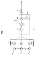
- Fig.1 is a block diagram for explaining the outline of a signal incoming direction estimation apparatus in an embodiment of the present invention.
- LPF low pass filter
- the RF down-converter 2 is provided with an impedance tuner (T) 21, a low noise amplifier 22, a mixer 23, and a local oscillator 24 and a signal (beat signal) in the baseband frequency band is obtained by mixing the received signal from the antenna unit 1 and the output signal (transmitting signal) of the local oscillator 24 in the mixer (frequency conversion section) 23 to carry out frequency conversion (down conversion). Prior to the frequency conversion, low-noise amplification of the received signal is also carried out by the LNA 22. Further, by means of the impedance tuner 21, the impedance of the feeding point can be adjusted.
- the wavelength of an RF signal is ⁇ .
- I K is a current induced by each of the antennas A RK
- N A 3
- the impedance of each of the antennas A R1 , A R2 , and A R3 is set to an appropriate value (so as to trace a constant reactance circle on the Smith chart, for example) in the respective matching circuits M K (M 1 , M 2 , M 3 ) and the impedance of the feeding point is adjusted y the impedance tuner 21 and matched to the matching circuits M 1 , M 2 , and M 3 sequentially, the distribution of I K changes in accordance with the matching state and as a result, it is possible to electronically scan beams (to control the beam direction).
- a beam scan is carried out by changing the current of each of the antennas A 0 , A 1 , and A 2 by manipulating the terminal impedances z 1 and z 2 of the passive antennas A 1 and A 2 , however, in the present embodiment, the terminal impedances z 1 and z 2 are fixed to certain values (the above-mentioned y 0 , y 1 , and y 2 : constant) and the impedances z 0 of the feeding point (feeding antenna A 0 ) is changed.
- the above-mentioned expressions (2.5) and (2.6) are modified to a certain extent and the following expression (2.7) is obtained.
- I v s z 0 + z 00 ⁇ z 01 ⁇ y 1 y 0 + z 02 ⁇ y 2 y 0 1 y 1 / y 0 y 2 / y 0
- the terminal impedances z 1 and z 2 of the passive antennas A 1 and A 2 may also be possible to make the terminal impedances z 1 and z 2 of the passive antennas A 1 and A 2 variable in addition to the impedance z 0 of the feeding antenna A 0 , which is a feeding point, in order to carry out a more flexible scan (beam scan) or a detailed directional control.
- the antenna unit (ULA) 1 having N A sensor elements (ant
- the RF down-converter 2 is provided with the impedance tuner 21, the LNA 22, the mixer 23, and the local oscillator 24 and a signal (beat signal) in the baseband frequency band is obtained by mixing the received signal from the antenna unit 1 and the output signal (transmitting signal) of the local oscillator 24 in the mixer 23 to carry out frequency conversion (down conversion).
- the low-noise amplification of the received signal is also carried out by the LNA 22.
- the impedance tuner 21 the current distribution of each of the antennas A k can be adjusted by adjusting the impedance of the feeding point.
- the impedance tuner 21 may take at least N A (for example, Z 1 *, Z 2 *, ..., Z NA *) or more states (impedances).
- N A for example, Z 1 *, Z 2 *, ..., Z NA *
- an apparatus such as a phase shifter that carries out the equivalent functions to the impedance tuner 21.
- the baseband unit 5 is provided with a demultiplexing section (DMUX) 51 and a low pass filter 52 the number of which corresponding to the number of antennas N A (N A is the number of channels), respectively, and the beat signals from the RF down-converter 2 are separated for each channel in the demultiplexing section 51 and each beat signal passes through its corresponding LPF 52, thereby a beat signal can be obtained for each channel.
- the beat signal obtained for each channel is input to a digital signal processor such as CPU, although not shown, and a required digital signal processing such as FFT is carried out.
- a switch that has employed a MEMS (Micro Electro Mechanical System) technique, which is capable of direct input/output port switching, and the loss of which is low is used.
- MEMS Micro Electro Mechanical System
- the antenna beam shows the maximum directionality in the direction of the second antenna.
- the impedance of the impedance tuner 21 it is possible to form (scan) the antenna beam so as to show the maximum directionality in the direction of the third, ..., or the N A -th antenna.
- the sensor array (ULA) 1 composed of N A antennas (sensors) A k
- a high-speed beam scan becomes possible by manipulating only one impedance (of the impedance tuner 21) after once designed. Compared to a switching beam former, it is possible to considerably reduce the number of IC ports due to the adjustable region of the tuner that can be realized.
- Fig.5 shows how the beam scan is carried out in the present embodiment.
- Fig.5 an example is shown, where the impedance of the impedance tuner 21 is changed into eight states, and it will be understood that it is possible to form a beam having eight peak gains in accordance with each state.
- Fig.6 is a block diagram showing a modified example of the essential parts of a wireless apparatus (beam former), which is a signal incoming direction estimation apparatus in an embodiment of the present invention.
- the construction of the wireless apparatus shown in Fig.6 differs from the construction shown in Fig.1 in that in the antenna unit (ULA) 1, N A wave detectors D k are provided in order to monitor the output power of each of the antennas A Rk and at the same time, a hybrid circuit (HYB) 6 for branching part of output of the LPF 3 in the post stage of the LPF 3, an A/D converter 7 for analog-to-digital converting each output of the above-mentioned wave detectors D k (or the output branched from the hybrid circuit 6) into a digital signal, and a CPU (control means) 8 for adaptively adjusting the impedance of the impedance tuner 21 in the RF down-converter 2 based on the digital output of the A/D converter 7 are added.
- the transmitting system is
- the output power of each of the antennas A Rk (or the output power of the RF down-converter 2) is monitored by the CPU 8 through each of the above-mentioned wave detectors D k (or the hybrid circuit 6) and the A/D converter 7, the impedance of the impedance tuner 21 is controlled (adjusted) adaptively so as to provide the maximum received power (or the minimum angular measurement error), and the amount of offset of the terminal impedance is adjusted. Due to this, it becomes possible to smooth the variations in manufacture of the antennas A Rk , etc.
- An optimum combination of the impedances of each of the above-mentioned matching circuits M k can be obtained by using an already-known neural network in which, for example, the impedance of each of the antennas A Rk and the impedance tuner 21 are regarded as an input and the received power or the measured angle are regarded as an output (for example, refer to K. Shirakawa, et al. "Structural Determination of Multilayered Large-Signal Neural-Network HEMT Model", IEEE TRANSACTIONS ON MICROWAVE THEORY AND TECHNIQUES, VOL. 46, NO.10, OCTOBER 1998 etc.)
- an optimum combination can also be obtained by associating the impedance values that each impedance can take with a series of numbers, assuming a virtual biotic group having these numbers as a chromosome, and applying a genetic algorithm on the assumption that the received power, the error rate, or the estimated angular error is the fitness of the individual in the biotic group.
- the impedance tuner (variable impedance adjustment means) selectively connected to any one of sensors (antennas) for controlling the current distribution of each sensor
Landscapes
- Physics & Mathematics (AREA)
- Engineering & Computer Science (AREA)
- General Physics & Mathematics (AREA)
- Radar, Positioning & Navigation (AREA)
- Remote Sensing (AREA)
- Variable-Direction Aerials And Aerial Arrays (AREA)
- Radar Systems Or Details Thereof (AREA)
Abstract
Description
- This application is based on and hereby claims priority to
Japanese Application No. 2005-149569 filed on May 23, 2005 - The present invention relates to a signal incoming direction estimation apparatus and, more particularly, to a technique suitable for use in a wireless system for detecting the incoming angle of a signal (electromagnetic wave) using a sensor array.
- Fig.7 shows a block diagram of an apparatus for estimating the incoming direction of electromagnetic waves as an example of a signal incoming direction estimation apparatus. The electromagnetic wave incoming direction estimation apparatus shown in Fig.7 employs a uniformly-spaced linear array antenna (hereinafter, abbreviated to ULA, occasionally) 100 the number of sensor elements (antennas) of which is NA (in this example, NA = 9) and the intervals of antennas of which are d as a receiving system, and estimates the incoming direction of electromagnetic waves by utilizing the fast Fourier transform (FFT). In other words, it is an FMCW (Frequency Modulated Continuous Wave) radar apparatus for detecting the azimuth of a target object by frequency-converting a beat signal obtained by mixing a transmitted signal and a received signal and carrying out a beam scan to the converted signal.
- The FMCW radar apparatus comprises, as its essential parts, the ULA 100 having NA elements (antennas) 101 arranged at uniform intervals (d), an RF down-
converter 200 for obtaining a beat signal in the baseband frequency band by mixing a signal (RF signal) received by theULA 100 and a transmitted RF signal and frequency-converting (down converting) it, a low pass filter (LPF) 300, and an A/D converter 400, and aCPU 500 as a receiving system, and at the same time, comprising a baseband oscillator (triangle wave oscillator) 600, an up-converter 700 for frequency-converting (up converting) a signal at the oscillation frequency (baseband frequency) of theoscillator 600 into an RF signal, and a transmittingantenna 800 as a transmitting system. - The ULA 100 is provided with
switches switches antenna 101 to receive a signal (to input the received signal into the RF down-converter 200) is switched to another in a time division manner as will be described later. The RF down-converter 200 has a low noise amplifier (LNA) 201 and amixer 202 and the received signal from theULA 100 is, after low-noise amplification by theLNA 201, mixed by themixer 202 with a signal from an RF voltage control oscillator 701 (that is, the transmitting RF signal) shared by the up-converter 700 and thus a beat signal in the baseband frequency band, that is, a signal having a delay time, a Doppler frequency shift, and a beat frequency determined by the relative distance and the relative velocity between the present radar apparatus and the target object can be obtained. - Further, in the transmitting system, the up-
converter 700 comprises the above-mentioned RF voltage control oscillator (RF-VCO) 701 driven by the output voltage signal (modulation control signal) of thebaseband oscillator 600 and outputting an RF signal (transmission modulation signal), a high power amplifier (HPA) 703 for amplifying the output of the RFvoltage control oscillator 701 to a predetermined signal level in accordance with the sensing distance, and a hybrid circuit (HYB) 702 for branching the output of the RFvoltage control oscillator 701 into two and supplying one to the HPA 703 and the other to themixer 202 of the RF down-converter 200. - Next, the operation of the radar apparatus constructed as described above, particularly, the operation of the receiving system is explained below. In the following explanation, each
antenna 101 shown in Fig. 7 is denoted by symbol Ak (k = 1 to NA) where A1 denotes thenearest antenna 101 to the transmitting antenna 800 (letting position of theantenna 101 be the origin) among theantennas 101 constituting thereceiving ULA 100 shown in Fig.7. - First, if it is assumed that Ns of independent signals xm (t) arrive at the
ULA 100 with angles θm (m = 1 to Ns) at time t, the phase difference between the signals xm (t) arriving at the antenna A1 and the antenna Ak is expressed by the following expression (1.1) with the origin being the phase reference.
- Therefore, the output vk (t) from the antenna Ak is expressed, along with the noise signal nk (t), by the following expression (1.2).

- However, it is assume that each signal is a baseband representation and that the direction of an incoming angle is positive if the direction is in the clockwise direction with respect to the Y-axis (0°).
- Next, it is assumed that the period of the signal Xm (t) is Tm, NT of samples taken in from each of the antennas Ak during the period Tm are vectorized into vk as shown in the following expression (1.3), and the Fourier transform thereof is Vk as shown in the following expression (1.4).


- However, Vk (1) (1 = 1 to NT) is expressed by the following expression (1.5) where the Fourier transform coefficients of Xm (t) and nk (t) are Xm (1) and Nk (1), respectively.

- Finally, if Vk (1) multiplied by exp (-jϕk q) and summed in terms of k is expressed by Vq (1), the following expression (1.6) is obtained,

where the inside of the brackets { } of the above-mentioned expression (1.6) is an array factor for m-th (m = 1 to Ns) signal expressed by the following expression (1.7), and it will be found that the in-phase condition is satisfied and there exists a peak when θq = θm.
- Therefore, if the above-mentioned expression (1.6) is calculated while changing 1 and θq, the position on the frequency index: 1 and the angle index: q of each signal source is known as the sum of the array factors weighted with the spectrum Xm (1) of the baseband signal. The calculation (digital signal processing) is carried out by the
CPU 500 for a beat signal having passed from the RF down-converter 200 through theLPF 300 and having been digitized by the A/D converter 400. - Here, it is necessary to realize pointed directional beams using a number of sensor elements (antennas) 101 in order to separate signal sources closely adj acent angularly to each other with a radar apparatus (signal incoming direction estimation apparatus) using the
ULA 100. In the frequency band for which the variations in the hardware performance and the cost cause no problem, the object can be attained by simply preparing the baseband generation circuits (the RF down-converter 200, theLPF 300, the A/D converter 400, etc., shown in Fig.7) of the same number as that of the sensor elements, but in the frequency band for which the above-mentioned problems cannot be ignored (for example, a millimeter wave band such as a 76 GHz band), it is a mandatory item required by the system development to reduce the number of baseband generation circuits. - Then, in the signal incoming direction estimation apparatus in such a frequency band, as shown in Fig.7, the above-mentioned
switches sensor elements 101 and these switches are switched at a certain timing to share the baseband generation circuit (the RF down-converter, theLPF 300, the A/D converter 400, etc.) in a time division manner and thereby the antenna beam is formed by the digital signal processing (this is referred also to as an electronic scan system). An example of this type of signal incoming direction estimation apparatus (switching beam former) is disclosed, for example, in the followingPatent Document 1.
[Patent Document 1]Japanese Patent Laid-Open (Kokai) HEI 6-281715 - However, in the above-described configuration, the following problems arise.
- (1) As the number NA of sensor elements increases, the simultaneity of the signals obtained from each of the
sensor elements 101 collapses and in particular, in such a case where the signal source is moving, there is the possibility that the original purpose of the apparatus to estimate the incoming direction cannot be attained. - (2) To realize the
switches switches LNA 201. - (3) Further, in order to avoid the electromagnetic interaction between the
switches switches - The above-mentioned problems being taken into consideration, the present invention has been developed and an object thereof is to provide a signal incoming direction estimation apparatus capable of obviating a switch for time division switching of antennas (sensors) and of carrying out a high-speed beam scan without manipulating all the sensor impedances.
- In order to attain the above-mentioned object, a signal incoming direction estimation apparatus of the present invention is:
- (1) characterized by comprising a sensor array having plural sensors and the impedance of each of the sensors being set to a predetermined value, respectively and a variable impedance adjustment means having a variable impedance, being selectively connected to any one of the sensors of the sensor array, and controlling the current distribution of each of the sensors.
- (2) Here, the signal incoming direction estimation apparatus may comprise a time division switch section for connecting each of the above-mentioned sensors to the variable impedance adjustment means in a time division manner.
- (3) Further, the sensor and the variable impedance adjustment means may be coupled electromagnetically.
- (4) The impedance of each of the sensors may be made variable.
- (5) The sensor array may be constructed as an ESPAR (Electronically Steerable Passive Array Radiator) type sensor array for electromagnetically coupling each of the sensors.
- (6) The signal incoming direction estimation apparatus may further comprise a monitor means for monitoring the output power of either or both of the output of each of the sensors and the output of the variable impedance adjustment means and a control means for adjusting the impedance of the variable impedance adjustment means based on the output power monitored by the monitor means.
- (7) The monitor means may be constructed so as to comprise a wave detector for detecting the output of each of the sensors.
- (8) The monitor means may be constructed so as to comprise a branch circuit for branching part of the output of the variable impedance adjustment means and inputting it into the control means.
- (9) The time division switch section may be constructed by using a MEMS (Micro Electro Mechanical System) technique.
- According to the present invention, it is possible to carry out a beam scan only by manipulating at least one of the impedances (of the impedance tuner) without simultaneously manipulating all the sensor impedances because the variable impedance adjustment means selectively connected to any one of the sensors and controlling the current distribution of each sensor is provided. Therefore, a high-speed beam scan (directional control) is possible. Further, the switch for time division switching of the sensors can be obviated.
- Furthermore, if the impedance of each of the above-mentioned sensors is made variable, a more flexible and more detailed beam scan can be realized.
-
- Fig.1 is a block diagram for explaining the outline of a signal incoming direction estimation apparatus in an embodiment of the present invention.
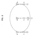
- Fig.2 is a diagram for explaining concrete example 1 of a signal incoming direction estimation apparatus in an embodiment of the present invention.
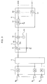
- Fig.3 is a diagram for explaining concrete example 2 of a signal incoming direction estimation apparatus in an embodiment of the present invention.
- Fig.4(A) and Fig.4(B) are both diagrams for explaining the operation of the signal incoming direction estimation apparatus shown in Fig.3.
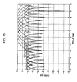
- Fig.5 is a diagram showing how a beam scan is carried out by a signal incoming direction estimation apparatus in an embodiment of the present invention.
- Fig.6 is a block diagram showing a modification example of an essential construction of a wireless apparatus (beam former), which is a signal incoming direction estimation apparatus in an embodiment of the present invention.
- Fig.7 is a diagram showing an example of a conventional signal incoming direction estimation apparatus.
- Hereinafter, embodiments of the present invention are explained with reference to drawings.
- Fig.1 is a block diagram for explaining the outline of a signal incoming direction estimation apparatus in an embodiment of the present invention. The signal incoming direction estimation apparatus shown in Fig.1 comprises, as a receiving system, an antenna unit (ULA) 1 forming an antenna array in which NA (NA=3 in Fig. 1) of sensor elements (antennas) ARK (k = 1 to NA) are arranged at element intervals d, an RF down-converter (frequency converter), for example, connected physically to or coupled electromagnetically to each of the antennas ARK of the
antenna unit 1, to which a radio signal received by any one of the antennas ARK is input, and down-converting the radio signal into a baseband signal, and a low pass filter (LPF) 3 for passing only the low-frequency components of the baseband signal from the RF down-converter 2 and removing unwanted noise components. The transmitting system is not shown schematically here. - The RF down-
converter 2 is provided with an impedance tuner (T) 21, alow noise amplifier 22, amixer 23, and alocal oscillator 24 and a signal (beat signal) in the baseband frequency band is obtained by mixing the received signal from theantenna unit 1 and the output signal (transmitting signal) of thelocal oscillator 24 in the mixer (frequency conversion section) 23 to carry out frequency conversion (down conversion). Prior to the frequency conversion, low-noise amplification of the received signal is also carried out by theLNA 22. Further, by means of theimpedance tuner 21, the impedance of the feeding point can be adjusted. - As described above, when NA of the antennas ARK arranged at the element intervals d form the array, the characteristics of the antenna array can be expressed by the following expression (2.1) where the current distribution of each of the antennas ARK is denoted by Ik (k = 1 to NA) and the wavelength of an RF signal is λ.

- Here, in expression (2.1), since IK is a current induced by each of the antennas ARK, when, for example, NA = 3, if the impedance of each of the antennas AR1, AR2, and AR3 is set to an appropriate value (so as to trace a constant reactance circle on the Smith chart, for example) in the respective matching circuits MK (M1, M2, M3) and the impedance of the feeding point is adjusted y the
impedance tuner 21 and matched to the matching circuits M1, M2, and M3 sequentially, the distribution of IK changes in accordance with the matching state and as a result, it is possible to electronically scan beams (to control the beam direction). - This operation will be made easier to understand if it is assumed that the operation is controlled by the electricity supply to the parallel resistors or an ESPAR (Electronically Steerable Passive Array Radiator) antenna is operated by source pull, and depending on the incoming direction estimation method or the adjustable range of the tuner that can be realized, it becomes possible to considerably reduce the number of IC ports.
- When NA + 1 (this denotation follows the denotation of antenna number of an ordinary ESPAR system) of antennas are arranged as shown in Fig.2 as the above-mentioned
antenna unit 1, in other words, when an ESPAR antenna in which passive antennas A1, A2, ... are arranged in the vicinity of an antenna (feeding antenna) A0 to which a feeding voltage Vs is supplied is applied, if it is assumed that an admittance matrix of the array antenna itself, seen from each antenna terminal, is
YA (not terminated), an impedance matrix consisting of terminal elements is
ZT = diag (z0, z1, ... ZNA), and further the antenna terminal voltage vector is V, and the current is I,
the following expressions (2.2) and (2.3) hold for U = (1, 0, ..., 0)t.

- Here, by substituting expression (2.2) into expression (2.3) and modifying expression (2.3) to a certain extent, the following expression is obtained.

- For simplicity of explanation, it is assumed that NA = 2 and YA -1 ≡ ZA, then,


- In an ordinary ESPAR antenna, in the case of Fig.2, a beam scan is carried out by changing the current of each of the antennas A0, A1, and A2 by manipulating the terminal impedances z1 and z2 of the passive antennas A1 and A2, however, in the present embodiment, the terminal impedances z1 and z2 are fixed to certain values (the above-mentioned y0, y1, and y2: constant) and the impedances z0 of the feeding point (feeding antenna A0) is changed. In order to make clear, the above-mentioned expressions (2.5) and (2.6) are modified to a certain extent and the following expression (2.7) is obtained.

- For example, if the impedance of the
impedance tuner 21 is set as the following expressions (2.8) and (2.9),

- By the way, as a matter of course, it may also be possible to make the terminal impedances z1 and z2 of the passive antennas A1 and A2 variable in addition to the impedance z0 of the feeding antenna A0, which is a feeding point, in order to carry out a more flexible scan (beam scan) or a detailed directional control.
- Next, a concrete example of the apparatus is explained with reference to Fig.3. Fig.3 is a block diagram showing essential parts of a wireless apparatus (beam former) as the signal incoming direction estimation apparatus of the present invention and the wireless apparatus shown in Fig. 3 comprises, as a receiving system, the antenna unit (ULA) 1 having NA sensor elements (antennas) Ak (k = 1 to NA) arranged at an element interval d, and having NA matching circuits Mk for setting the impedance of each of the antennas Ak to an appropriate value, a
switch section 4 for selectively (in a time division manner) outputting the radio signal received by each of the antennas Ak (that is, each of the antennas Ak is selectively connected to the RF down-converter 2 in the post stage in a one-to-one manner), the RF down-converter (frequency converter) 2 for frequency-converting (down converting) the received signal (RF signal) from theswitch section 4 into the baseband signal, and abaseband unit 5 for separating the output (baseband signal) of the RF down-converter 2 for each of NA channels. The transmitting system is not shown here. - In the present embodiment also, the RF down-
converter 2 is provided with theimpedance tuner 21, theLNA 22, themixer 23, and thelocal oscillator 24 and a signal (beat signal) in the baseband frequency band is obtained by mixing the received signal from theantenna unit 1 and the output signal (transmitting signal) of thelocal oscillator 24 in themixer 23 to carry out frequency conversion (down conversion). Prior to the frequency conversion, the low-noise amplification of the received signal is also carried out by theLNA 22. Further, by means of theimpedance tuner 21, the current distribution of each of the antennas Ak can be adjusted by adjusting the impedance of the feeding point. Here it is possible for theimpedance tuner 21 to take at least NA (for example, Z1*, Z2*, ..., ZNA*) or more states (impedances). By the way, it may be possible to apply, in place of theimpedance tuner 21, an apparatus such as a phase shifter that carries out the equivalent functions to theimpedance tuner 21. - Further, the
baseband unit 5 is provided with a demultiplexing section (DMUX) 51 and alow pass filter 52 the number of which corresponding to the number of antennas NA (NA is the number of channels), respectively, and the beat signals from the RF down-converter 2 are separated for each channel in thedemultiplexing section 51 and each beat signal passes through itscorresponding LPF 52, thereby a beat signal can be obtained for each channel. The beat signal obtained for each channel is input to a digital signal processor such as CPU, although not shown, and a required digital signal processing such as FFT is carried out. - As the
switch section 4, a switch that has employed a MEMS (Micro Electro Mechanical System) technique, which is capable of direct input/output port switching, and the loss of which is low is used. - Here, the operation is explained with reference to Fig.4 (A) and Fig. 4 (B) on the assumption that the impedance of each of the antennas Ak seen from the RF down-
converter 2 is Z1 to ZNA by the matching circuits M1 to MN and for simplicity, Z1 = R + jX, Z2 = R + j2X, ..., ZNA = R + jNAX. Here Fig.4 (A) and Fig.4 (B) each show a case where NA = 2. - First, as shown in Fig. 4 (A), if the impedance of the
impedance tuner 21 is set to Z1* and the first antenna A1 is selected by theswitch section 4, the antenna current is I1 = V1/2R, and if the second, ..., or the NA-th antenna ANA is selected, the antenna current is I2 = V1/ [2R + jX] , ..., or IN = V1/ [2R + j(NA-1)X], therefore, in this case, the antenna beam shows the maximum directionality in the direction of the first antenna. - Further, as shown in Fig. 4 (B), if the impedance of the
impedance tuner 21 is set to Z2* then considering in the same manner, the respective antenna currents are I1 = V1 / [2R - jX], I2 = V1 / 2R, ..., IN = V1 / [2R + j(NA - 2)X], and in this case, the antenna beam shows the maximum directionality in the direction of the second antenna. Similarly, by changing the impedance of theimpedance tuner 21, it is possible to form (scan) the antenna beam so as to show the maximum directionality in the direction of the third, ..., or the NA-th antenna. - As described above, in the sensor array (ULA) 1 composed of NA antennas (sensors) Ak, it is possible to adjust the current distribution of each of the sensors Ak to carry out the beam scan of the sensor array by setting the respective sensor impedances to respective appropriate values (predetermined values) in advance or adaptively, arranging the
impedance tuner 21 capable of taking at least NA states (impedances) or more between theULA 1 and the down-converter 2 (mixer 23), and manipulating the impedance of thetuner 21. - Therefore, while it is necessary for an ordinary ESPAR beam former to simultaneously manipulate the NA sensor impedances, in the present embodiment, a high-speed beam scan becomes possible by manipulating only one impedance (of the impedance tuner 21) after once designed. Compared to a switching beam former, it is possible to considerably reduce the number of IC ports due to the adjustable region of the tuner that can be realized.
- Fig.5 shows how the beam scan is carried out in the present embodiment. In Fig.5, an example is shown, where the impedance of the
impedance tuner 21 is changed into eight states, and it will be understood that it is possible to form a beam having eight peak gains in accordance with each state. - Fig.6 is a block diagram showing a modified example of the essential parts of a wireless apparatus (beam former), which is a signal incoming direction estimation apparatus in an embodiment of the present invention. The construction of the wireless apparatus shown in Fig.6 differs from the construction shown in Fig.1 in that in the antenna unit (ULA) 1, NA wave detectors Dk are provided in order to monitor the output power of each of the antennas ARk and at the same time, a hybrid circuit (HYB) 6 for branching part of output of the
LPF 3 in the post stage of theLPF 3, an A/D converter 7 for analog-to-digital converting each output of the above-mentioned wave detectors Dk (or the output branched from the hybrid circuit 6) into a digital signal, and a CPU (control means) 8 for adaptively adjusting the impedance of theimpedance tuner 21 in the RF down-converter 2 based on the digital output of the A/D converter 7 are added. In Fig.6 also, the transmitting system is not shown. In Fig.6, the parts to which the same symbols as those already described are attached are the same as or similar to those already described unless otherwise specified. - In the wireless apparatus (beam former) in the present embodiment constructed as described above, the output power of each of the antennas ARk (or the output power of the RF down-converter 2) is monitored by the
CPU 8 through each of the above-mentioned wave detectors Dk (or the hybrid circuit 6) and the A/D converter 7, the impedance of theimpedance tuner 21 is controlled (adjusted) adaptively so as to provide the maximum received power (or the minimum angular measurement error), and the amount of offset of the terminal impedance is adjusted. Due to this, it becomes possible to smooth the variations in manufacture of the antennas ARk, etc. - An optimum combination of the impedances of each of the above-mentioned matching circuits Mk can be obtained by using an already-known neural network in which, for example, the impedance of each of the antennas ARk and the
impedance tuner 21 are regarded as an input and the received power or the measured angle are regarded as an output (for example, refer to K. Shirakawa, et al. "Structural Determination of Multilayered Large-Signal Neural-Network HEMT Model", IEEE TRANSACTIONS ON MICROWAVE THEORY AND TECHNIQUES, VOL. 46, NO.10, OCTOBER 1998 etc.) - Further, in a construction in which the setting of the impedances of each of the antennas ARk and the
impedance tuner 21 is carried out digitally, an optimum combination can also be obtained by associating the impedance values that each impedance can take with a series of numbers, assuming a virtual biotic group having these numbers as a chromosome, and applying a genetic algorithm on the assumption that the received power, the error rate, or the estimated angular error is the fitness of the individual in the biotic group. - The present invention is not limited to the embodiments described above and it is needless to say that various modifications can be embodied without departing from the concept of the present invention.
- As described above in detail, according to the present invention, since the impedance tuner (variable impedance adjustment means) selectively connected to any one of sensors (antennas) for controlling the current distribution of each sensor is provided, it is possible to carry out a beam scan only by manipulating at least one impedance (of the impedance tuner) without simultaneously manipulating all the sensor impedances. Therefore, a high-speed beam scan is possible and the present invention is thought to be extremely useful in the radio communication technique field, particularly, in the mobile radio communication and radar technique fields.
Claims (9)
- A signal incoming direction estimation apparatus characterized by comprising:a sensor array (1) having plural sensors (ARk: k = 1 to NA) and the impedance of each of said sensors (ARk) being set to a predetermined value (Mk), respectively; anda variable impedance adjustment means (21) having a variable impedance, being selectively connected to any one of the sensors (ARk) of said sensor array (1), and controlling the current distribution (Ik) of each of said sensors (ARk).
- The signal incoming direction estimation apparatus according to claim 1, characterized by further comprising a time division switch section (4) for connecting each of said sensors (ARk) to said variable impedance adjustment means (21) in a time division manner.
- The signal incoming direction estimation apparatus according to claim 1, characterized in that said sensor (ARk) and said variable impedance adjustment means (21) are coupled electromagnetically.
- The signal incoming direction estimation apparatus according to any one of claims 1 to 3, characterized in that the impedance (Mk) of each of said sensors (ARk) is also variable.
- The signal incoming direction estimation apparatus according to any one of claims 1 to 4, characterized in that said sensor array (1) is constructed as an ESPAR (Electronically Steerable Passive Array Radiator) type sensor array for electromagnetically coupling each of said sensors (ARk).
- The signal incoming direction estimation apparatus according to any one of claims 1 to 5, characterized by further comprising:a monitor means for monitoring the output power of either or both of the output of each of said sensors (ARk) and the output of said variable impedance adjustment means (21) ; anda control means (8) for adjusting the impedance of said variable impedance adjustment means (21) based on the output power monitored by said monitor means.
- The signal incoming direction estimation apparatus according to claim 6, characterized in that said monitor means is constructed so as to comprise a wave detector (Dk) for detecting the output of each of said sensors (ARk) .
- The signal incoming direction estimation apparatus according to claim 6 or 7, characterized in that said monitor means is constructed so as to comprise a branch circuit (6) for branching part of the output of said variable impedance adjustment means (21) and inputting it into said control means (8).
- The signal incoming direction estimation apparatus according to claim 2, characterized in that said time division switch section is constructed by using a MEMS (Micro Electro Mechanical System) technique.
Applications Claiming Priority (1)
| Application Number | Priority Date | Filing Date | Title |
|---|---|---|---|
| JP2005149569A JP4755849B2 (en) | 2005-05-23 | 2005-05-23 | Signal arrival direction estimation device |
Publications (2)
| Publication Number | Publication Date |
|---|---|
| EP1739448A1 true EP1739448A1 (en) | 2007-01-03 |
| EP1739448B1 EP1739448B1 (en) | 2011-03-09 |
Family
ID=36178053
Family Applications (1)
| Application Number | Title | Priority Date | Filing Date |
|---|---|---|---|
| EP05018477A Expired - Lifetime EP1739448B1 (en) | 2005-05-23 | 2005-08-25 | Apparatus for the determination of an incoming signal |
Country Status (4)
| Country | Link |
|---|---|
| US (1) | US7501959B2 (en) |
| EP (1) | EP1739448B1 (en) |
| JP (1) | JP4755849B2 (en) |
| DE (1) | DE602005026792D1 (en) |
Families Citing this family (21)
| Publication number | Priority date | Publication date | Assignee | Title |
|---|---|---|---|---|
| US8249523B2 (en) * | 2009-02-09 | 2012-08-21 | Broadcom Corporation | Method and system for a multi-port distributed antenna |
| DE102009027003A1 (en) * | 2009-06-17 | 2010-12-23 | Endress + Hauser Gmbh + Co. Kg | Optimization of the switching sequence in switched antenna arrays |
| JP5604746B2 (en) * | 2009-09-16 | 2014-10-15 | Necソリューションイノベータ株式会社 | Radio wave arrival direction estimation apparatus and radio wave arrival direction estimation method |
| US8811911B2 (en) * | 2010-07-02 | 2014-08-19 | Htc Corporation | Radio-frequency processing device and method and related wireless communication device |
| TWI431935B (en) * | 2010-09-28 | 2014-03-21 | Htc Corp | Antenna module |
| US9275690B2 (en) | 2012-05-30 | 2016-03-01 | Tahoe Rf Semiconductor, Inc. | Power management in an electronic system through reducing energy usage of a battery and/or controlling an output power of an amplifier thereof |
| US9509351B2 (en) | 2012-07-27 | 2016-11-29 | Tahoe Rf Semiconductor, Inc. | Simultaneous accommodation of a low power signal and an interfering signal in a radio frequency (RF) receiver |
| US9184498B2 (en) | 2013-03-15 | 2015-11-10 | Gigoptix, Inc. | Extending beamforming capability of a coupled voltage controlled oscillator (VCO) array during local oscillator (LO) signal generation through fine control of a tunable frequency of a tank circuit of a VCO thereof |
| US9531070B2 (en) | 2013-03-15 | 2016-12-27 | Christopher T. Schiller | Extending beamforming capability of a coupled voltage controlled oscillator (VCO) array during local oscillator (LO) signal generation through accommodating differential coupling between VCOs thereof |
| US9716315B2 (en) | 2013-03-15 | 2017-07-25 | Gigpeak, Inc. | Automatic high-resolution adaptive beam-steering |
| US9722310B2 (en) | 2013-03-15 | 2017-08-01 | Gigpeak, Inc. | Extending beamforming capability of a coupled voltage controlled oscillator (VCO) array during local oscillator (LO) signal generation through frequency multiplication |
| US9837714B2 (en) | 2013-03-15 | 2017-12-05 | Integrated Device Technology, Inc. | Extending beamforming capability of a coupled voltage controlled oscillator (VCO) array during local oscillator (LO) signal generation through a circular configuration thereof |
| US9666942B2 (en) | 2013-03-15 | 2017-05-30 | Gigpeak, Inc. | Adaptive transmit array for beam-steering |
| US9780449B2 (en) | 2013-03-15 | 2017-10-03 | Integrated Device Technology, Inc. | Phase shift based improved reference input frequency signal injection into a coupled voltage controlled oscillator (VCO) array during local oscillator (LO) signal generation to reduce a phase-steering requirement during beamforming |
| KR102601371B1 (en) * | 2015-12-18 | 2023-11-13 | 한국전자통신연구원 | Method and apparatus for mapping baseband signal into beamspace |
| US9853706B2 (en) * | 2015-12-18 | 2017-12-26 | Electronics And Telecommunications Research Institute | Method and apparatus for mapping baseband signal into beamspace |
| US10241187B2 (en) | 2015-12-24 | 2019-03-26 | Panasonic Intellectual Property Management Co., Ltd. | Position sensor, direction estimation method, and system |
| US10914829B2 (en) * | 2017-01-27 | 2021-02-09 | Panasonic Intellectual Property Management Co., Ltd. | Positioning sensor, sensor, and method |
| JP6738778B2 (en) | 2017-08-24 | 2020-08-12 | 株式会社Soken | Radar equipment |
| CN114444643B (en) * | 2019-04-17 | 2024-08-06 | 苹果公司 | Wireless locatable tags |
| FR3107963B1 (en) * | 2020-03-05 | 2023-06-30 | Continental Automotive | METHOD FOR ULTRA HIGH FREQUENCY CONTINUOUS COMMUNICATION AND LOCATION OF A PORTABLE "HANDS-FREE" ACCESS DEVICE TO A MOTOR VEHICLE |
Citations (2)
| Publication number | Priority date | Publication date | Assignee | Title |
|---|---|---|---|---|
| JPH06281715A (en) | 1992-12-25 | 1994-10-07 | Tele Syst:Kk | Device for measuring incoming direction of radio wave |
| JP2003304112A (en) * | 2002-04-09 | 2003-10-24 | Advanced Telecommunication Research Institute International | Array antenna control method and control device |
Family Cites Families (12)
| Publication number | Priority date | Publication date | Assignee | Title |
|---|---|---|---|---|
| JPH10126137A (en) * | 1996-10-14 | 1998-05-15 | Nippon Telegr & Teleph Corp <Ntt> | Antenna device |
| US6008760A (en) * | 1997-05-23 | 1999-12-28 | Genghis Comm | Cancellation system for frequency reuse in microwave communications |
| US7049933B1 (en) * | 2000-08-25 | 2006-05-23 | Rf Code, Inc. | Identification device detection using multiple signal combination |
| JP3587185B2 (en) * | 2001-09-28 | 2004-11-10 | オムロン株式会社 | Inductive wireless antenna and non-contact data communication device using the same |
| US6917337B2 (en) * | 2002-06-05 | 2005-07-12 | Fujitsu Limited | Adaptive antenna unit for mobile terminal |
| US6903656B1 (en) * | 2003-05-27 | 2005-06-07 | Applied Wireless Identifications Group, Inc. | RFID reader with multiple antenna selection and automated antenna matching |
| JP3931849B2 (en) * | 2003-07-10 | 2007-06-20 | ソニー株式会社 | Antenna device |
| US7148803B2 (en) * | 2003-10-24 | 2006-12-12 | Symbol Technologies, Inc. | Radio frequency identification (RFID) based sensor networks |
| US7095311B2 (en) * | 2003-11-25 | 2006-08-22 | The Regents Of The University Of California | Identification coding schemes for modulated reflectance systems |
| JP3974584B2 (en) * | 2004-01-22 | 2007-09-12 | 株式会社東芝 | Array antenna device |
| US7119738B2 (en) * | 2004-03-01 | 2006-10-10 | Symbol Technologies, Inc. | Object location system and method using RFID |
| JP4833534B2 (en) * | 2004-09-29 | 2011-12-07 | 富士通株式会社 | Radar equipment |
-
2005
- 2005-05-23 JP JP2005149569A patent/JP4755849B2/en not_active Expired - Fee Related
- 2005-08-25 EP EP05018477A patent/EP1739448B1/en not_active Expired - Lifetime
- 2005-08-25 DE DE602005026792T patent/DE602005026792D1/en not_active Expired - Lifetime
- 2005-08-26 US US11/212,288 patent/US7501959B2/en not_active Expired - Fee Related
Patent Citations (2)
| Publication number | Priority date | Publication date | Assignee | Title |
|---|---|---|---|---|
| JPH06281715A (en) | 1992-12-25 | 1994-10-07 | Tele Syst:Kk | Device for measuring incoming direction of radio wave |
| JP2003304112A (en) * | 2002-04-09 | 2003-10-24 | Advanced Telecommunication Research Institute International | Array antenna control method and control device |
Non-Patent Citations (3)
| Title |
|---|
| K. SHIRAKAWA: "Structural Determination of Multilayered Large-Signal Neural-Network HEMT Model", IEEE TRANSACTIONS ON MICROWAVE THEORY AND TECHNIQUES, vol. 46, no. 10, October 1998 (1998-10-01), XP011037311 |
| PATENT ABSTRACTS OF JAPAN vol. 2003, no. 12 5 December 2003 (2003-12-05) * |
| THIEL D V: "Switched parasitic antennas and controlled reactance parasitic antennas: a systems comparison", ANTENNAS AND PROPAGATION SOCIETY SYMPOSIUM, 2004. IEEE MONTEREY, CA, USA JUNE 20-25, 2004, PISCATAWAY, NJ, USA,IEEE, vol. 3, 20 June 2004 (2004-06-20), pages 3211 - 3214, XP010722068, ISBN: 0-7803-8302-8 * |
Also Published As
| Publication number | Publication date |
|---|---|
| DE602005026792D1 (en) | 2011-04-21 |
| US7501959B2 (en) | 2009-03-10 |
| EP1739448B1 (en) | 2011-03-09 |
| JP4755849B2 (en) | 2011-08-24 |
| JP2006329658A (en) | 2006-12-07 |
| US20060261968A1 (en) | 2006-11-23 |
Similar Documents
| Publication | Publication Date | Title |
|---|---|---|
| US7501959B2 (en) | Signal incoming direction estimation apparatus | |
| US6690952B2 (en) | Adaptive array antenna transceiver apparatus | |
| JP3525426B2 (en) | Radar equipment | |
| US7683833B2 (en) | Phase shifting and combining architecture for phased arrays | |
| AU2019426474A1 (en) | Antenna device and radar device | |
| JPH11231040A (en) | Radar equipment | |
| US6630905B1 (en) | System and method for redirecting a signal using phase conjugation | |
| WO2007083479A1 (en) | Radar apparatus | |
| US6853691B1 (en) | Vector modulator using amplitude invariant phase shifter | |
| JP4245794B2 (en) | Transmission directivity correction apparatus and transmission directivity correction method | |
| US12592494B2 (en) | Reconfigurable intelligent surface, RIS, with sensing capabilities and method for operating the same | |
| US12341257B2 (en) | Phased array antenna, transmission apparatus, radio-power transmission system and radio communication system | |
| Umar et al. | Antenna-duplexed passive beamforming front-end for joint communication and sensing | |
| Dong et al. | Low complexity on-board vector calibration network for optimal microwave wireless power transmission and enhanced RF-to-DC conversion efficiency | |
| US8106825B1 (en) | Distributed receiver | |
| JP3589605B2 (en) | Adaptive array antenna transceiver | |
| CN115327521B (en) | A phased array radar | |
| Choi et al. | Experiments on DOA-estimation and beamforming for 60 GHz smart antennas | |
| JP2000068730A (en) | Antenna device | |
| CN115372906B (en) | Microwave photon radar system based on leaky-wave antenna and target object detection method | |
| JPH11271436A (en) | Pulse Doppler radar device | |
| EP4206720B1 (en) | Beam shaping array for compact dual-range automotive radar | |
| Moldovan et al. | W-band substrate integrated waveguide radar sensor based on multi-port technology | |
| Hutu et al. | A 2.4 GHz active phase shifter architecture for smart antennas control | |
| Tosovsky | Software defined phased array antenna architecture and design approach |
Legal Events
| Date | Code | Title | Description |
|---|---|---|---|
| PUAI | Public reference made under article 153(3) epc to a published international application that has entered the european phase |
Free format text: ORIGINAL CODE: 0009012 |
|
| AK | Designated contracting states |
Kind code of ref document: A1 Designated state(s): AT BE BG CH CY CZ DE DK EE ES FI FR GB GR HU IE IS IT LI LT LU LV MC NL PL PT RO SE SI SK TR |
|
| AX | Request for extension of the european patent |
Extension state: AL BA HR MK YU |
|
| 17P | Request for examination filed |
Effective date: 20070308 |
|
| 17Q | First examination report despatched |
Effective date: 20070522 |
|
| AKX | Designation fees paid |
Designated state(s): DE FR GB |
|
| GRAP | Despatch of communication of intention to grant a patent |
Free format text: ORIGINAL CODE: EPIDOSNIGR1 |
|
| GRAS | Grant fee paid |
Free format text: ORIGINAL CODE: EPIDOSNIGR3 |
|
| GRAA | (expected) grant |
Free format text: ORIGINAL CODE: 0009210 |
|
| AK | Designated contracting states |
Kind code of ref document: B1 Designated state(s): DE FR GB |
|
| REG | Reference to a national code |
Ref country code: GB Ref legal event code: FG4D |
|
| REF | Corresponds to: |
Ref document number: 602005026792 Country of ref document: DE Date of ref document: 20110421 Kind code of ref document: P |
|
| REG | Reference to a national code |
Ref country code: DE Ref legal event code: R096 Ref document number: 602005026792 Country of ref document: DE Effective date: 20110421 |
|
| PLBE | No opposition filed within time limit |
Free format text: ORIGINAL CODE: 0009261 |
|
| STAA | Information on the status of an ep patent application or granted ep patent |
Free format text: STATUS: NO OPPOSITION FILED WITHIN TIME LIMIT |
|
| 26N | No opposition filed |
Effective date: 20111212 |
|
| REG | Reference to a national code |
Ref country code: DE Ref legal event code: R097 Ref document number: 602005026792 Country of ref document: DE Effective date: 20111212 |
|
| REG | Reference to a national code |
Ref country code: FR Ref legal event code: PLFP Year of fee payment: 11 |
|
| PGFP | Annual fee paid to national office [announced via postgrant information from national office to epo] |
Ref country code: GB Payment date: 20150819 Year of fee payment: 11 Ref country code: DE Payment date: 20150818 Year of fee payment: 11 |
|
| PGFP | Annual fee paid to national office [announced via postgrant information from national office to epo] |
Ref country code: FR Payment date: 20150629 Year of fee payment: 11 |
|
| REG | Reference to a national code |
Ref country code: DE Ref legal event code: R119 Ref document number: 602005026792 Country of ref document: DE |
|
| GBPC | Gb: european patent ceased through non-payment of renewal fee |
Effective date: 20160825 |
|
| REG | Reference to a national code |
Ref country code: FR Ref legal event code: ST Effective date: 20170428 |
|
| PG25 | Lapsed in a contracting state [announced via postgrant information from national office to epo] |
Ref country code: DE Free format text: LAPSE BECAUSE OF NON-PAYMENT OF DUE FEES Effective date: 20170301 Ref country code: FR Free format text: LAPSE BECAUSE OF NON-PAYMENT OF DUE FEES Effective date: 20160831 Ref country code: GB Free format text: LAPSE BECAUSE OF NON-PAYMENT OF DUE FEES Effective date: 20160825 |