EP1734576A1 - Semiconductor device having through electrode and method of manufacturing the same - Google Patents
Semiconductor device having through electrode and method of manufacturing the same Download PDFInfo
- Publication number
- EP1734576A1 EP1734576A1 EP06012546A EP06012546A EP1734576A1 EP 1734576 A1 EP1734576 A1 EP 1734576A1 EP 06012546 A EP06012546 A EP 06012546A EP 06012546 A EP06012546 A EP 06012546A EP 1734576 A1 EP1734576 A1 EP 1734576A1
- Authority
- EP
- European Patent Office
- Prior art keywords
- electrode
- insulating film
- substrate
- forming
- hole
- Prior art date
- Legal status (The legal status is an assumption and is not a legal conclusion. Google has not performed a legal analysis and makes no representation as to the accuracy of the status listed.)
- Withdrawn
Links
Images


Classifications
-
- H—ELECTRICITY
- H10—SEMICONDUCTOR DEVICES; ELECTRIC SOLID-STATE DEVICES NOT OTHERWISE PROVIDED FOR
- H10W—GENERIC PACKAGES, INTERCONNECTIONS, CONNECTORS OR OTHER CONSTRUCTIONAL DETAILS OF DEVICES COVERED BY CLASS H10
- H10W20/00—Interconnections in chips, wafers or substrates
- H10W20/01—Manufacture or treatment
- H10W20/021—Manufacture or treatment of interconnections within wafers or substrates
- H10W20/023—Manufacture or treatment of interconnections within wafers or substrates the interconnections being through-semiconductor vias
-
- H—ELECTRICITY
- H05—ELECTRIC TECHNIQUES NOT OTHERWISE PROVIDED FOR
- H05K—PRINTED CIRCUITS; CASINGS OR CONSTRUCTIONAL DETAILS OF ELECTRIC APPARATUS; MANUFACTURE OF ASSEMBLAGES OF ELECTRICAL COMPONENTS
- H05K3/00—Apparatus or processes for manufacturing printed circuits
- H05K3/40—Forming printed elements for providing electric connections to or between printed circuits
- H05K3/42—Plated through-holes or plated via connections
-
- H—ELECTRICITY
- H05—ELECTRIC TECHNIQUES NOT OTHERWISE PROVIDED FOR
- H05K—PRINTED CIRCUITS; CASINGS OR CONSTRUCTIONAL DETAILS OF ELECTRIC APPARATUS; MANUFACTURE OF ASSEMBLAGES OF ELECTRICAL COMPONENTS
- H05K3/00—Apparatus or processes for manufacturing printed circuits
- H05K3/44—Manufacturing insulated metal core circuits or other insulated electrically conductive core circuits
-
- H—ELECTRICITY
- H10—SEMICONDUCTOR DEVICES; ELECTRIC SOLID-STATE DEVICES NOT OTHERWISE PROVIDED FOR
- H10W—GENERIC PACKAGES, INTERCONNECTIONS, CONNECTORS OR OTHER CONSTRUCTIONAL DETAILS OF DEVICES COVERED BY CLASS H10
- H10W20/00—Interconnections in chips, wafers or substrates
- H10W20/01—Manufacture or treatment
- H10W20/021—Manufacture or treatment of interconnections within wafers or substrates
- H10W20/023—Manufacture or treatment of interconnections within wafers or substrates the interconnections being through-semiconductor vias
- H10W20/0238—Manufacture or treatment of interconnections within wafers or substrates the interconnections being through-semiconductor vias comprising etching via holes through pads or through electrodes
-
- H—ELECTRICITY
- H10—SEMICONDUCTOR DEVICES; ELECTRIC SOLID-STATE DEVICES NOT OTHERWISE PROVIDED FOR
- H10W—GENERIC PACKAGES, INTERCONNECTIONS, CONNECTORS OR OTHER CONSTRUCTIONAL DETAILS OF DEVICES COVERED BY CLASS H10
- H10W20/00—Interconnections in chips, wafers or substrates
- H10W20/01—Manufacture or treatment
- H10W20/021—Manufacture or treatment of interconnections within wafers or substrates
- H10W20/023—Manufacture or treatment of interconnections within wafers or substrates the interconnections being through-semiconductor vias
- H10W20/0261—Manufacture or treatment of interconnections within wafers or substrates the interconnections being through-semiconductor vias characterised by the filling method or the material of the conductive fill
-
- H—ELECTRICITY
- H10—SEMICONDUCTOR DEVICES; ELECTRIC SOLID-STATE DEVICES NOT OTHERWISE PROVIDED FOR
- H10W—GENERIC PACKAGES, INTERCONNECTIONS, CONNECTORS OR OTHER CONSTRUCTIONAL DETAILS OF DEVICES COVERED BY CLASS H10
- H10W20/00—Interconnections in chips, wafers or substrates
- H10W20/20—Interconnections within wafers or substrates, e.g. through-silicon vias [TSV]
-
- H—ELECTRICITY
- H10—SEMICONDUCTOR DEVICES; ELECTRIC SOLID-STATE DEVICES NOT OTHERWISE PROVIDED FOR
- H10P—GENERIC PROCESSES OR APPARATUS FOR THE MANUFACTURE OR TREATMENT OF DEVICES COVERED BY CLASS H10
- H10P14/00—Formation of materials, e.g. in the shape of layers or pillars
- H10P14/40—Formation of materials, e.g. in the shape of layers or pillars of conductive or resistive materials
- H10P14/46—Formation of materials, e.g. in the shape of layers or pillars of conductive or resistive materials using a liquid
- H10P14/47—Electrolytic deposition, i.e. electroplating; Electroless plating
-
- H—ELECTRICITY
- H10—SEMICONDUCTOR DEVICES; ELECTRIC SOLID-STATE DEVICES NOT OTHERWISE PROVIDED FOR
- H10W—GENERIC PACKAGES, INTERCONNECTIONS, CONNECTORS OR OTHER CONSTRUCTIONAL DETAILS OF DEVICES COVERED BY CLASS H10
- H10W70/00—Package substrates; Interposers; Redistribution layers [RDL]
- H10W70/60—Insulating or insulated package substrates; Interposers; Redistribution layers
- H10W70/62—Insulating or insulated package substrates; Interposers; Redistribution layers characterised by their interconnections
- H10W70/65—Shapes or dispositions of interconnections
-
- H—ELECTRICITY
- H10—SEMICONDUCTOR DEVICES; ELECTRIC SOLID-STATE DEVICES NOT OTHERWISE PROVIDED FOR
- H10W—GENERIC PACKAGES, INTERCONNECTIONS, CONNECTORS OR OTHER CONSTRUCTIONAL DETAILS OF DEVICES COVERED BY CLASS H10
- H10W70/00—Package substrates; Interposers; Redistribution layers [RDL]
- H10W70/60—Insulating or insulated package substrates; Interposers; Redistribution layers
- H10W70/62—Insulating or insulated package substrates; Interposers; Redistribution layers characterised by their interconnections
- H10W70/65—Shapes or dispositions of interconnections
- H10W70/654—Top-view layouts
- H10W70/656—Fan-in layouts
-
- H—ELECTRICITY
- H10—SEMICONDUCTOR DEVICES; ELECTRIC SOLID-STATE DEVICES NOT OTHERWISE PROVIDED FOR
- H10W—GENERIC PACKAGES, INTERCONNECTIONS, CONNECTORS OR OTHER CONSTRUCTIONAL DETAILS OF DEVICES COVERED BY CLASS H10
- H10W72/00—Interconnections or connectors in packages
- H10W72/01—Manufacture or treatment
- H10W72/019—Manufacture or treatment of bond pads
-
- H—ELECTRICITY
- H10—SEMICONDUCTOR DEVICES; ELECTRIC SOLID-STATE DEVICES NOT OTHERWISE PROVIDED FOR
- H10W—GENERIC PACKAGES, INTERCONNECTIONS, CONNECTORS OR OTHER CONSTRUCTIONAL DETAILS OF DEVICES COVERED BY CLASS H10
- H10W72/00—Interconnections or connectors in packages
- H10W72/071—Connecting or disconnecting
- H10W72/072—Connecting or disconnecting of bump connectors
- H10W72/07251—Connecting or disconnecting of bump connectors characterised by changes in properties of the bump connectors during connecting
-
- H—ELECTRICITY
- H10—SEMICONDUCTOR DEVICES; ELECTRIC SOLID-STATE DEVICES NOT OTHERWISE PROVIDED FOR
- H10W—GENERIC PACKAGES, INTERCONNECTIONS, CONNECTORS OR OTHER CONSTRUCTIONAL DETAILS OF DEVICES COVERED BY CLASS H10
- H10W72/00—Interconnections or connectors in packages
- H10W72/20—Bump connectors, e.g. solder bumps or copper pillars; Dummy bumps; Thermal bumps
-
- H—ELECTRICITY
- H10—SEMICONDUCTOR DEVICES; ELECTRIC SOLID-STATE DEVICES NOT OTHERWISE PROVIDED FOR
- H10W—GENERIC PACKAGES, INTERCONNECTIONS, CONNECTORS OR OTHER CONSTRUCTIONAL DETAILS OF DEVICES COVERED BY CLASS H10
- H10W72/00—Interconnections or connectors in packages
- H10W72/851—Dispositions of multiple connectors or interconnections
- H10W72/874—On different surfaces
- H10W72/884—Die-attach connectors and bond wires
-
- H—ELECTRICITY
- H10—SEMICONDUCTOR DEVICES; ELECTRIC SOLID-STATE DEVICES NOT OTHERWISE PROVIDED FOR
- H10W—GENERIC PACKAGES, INTERCONNECTIONS, CONNECTORS OR OTHER CONSTRUCTIONAL DETAILS OF DEVICES COVERED BY CLASS H10
- H10W72/00—Interconnections or connectors in packages
- H10W72/90—Bond pads, in general
- H10W72/921—Structures or relative sizes of bond pads
- H10W72/922—Bond pads being integral with underlying chip-level interconnections
- H10W72/9223—Bond pads being integral with underlying chip-level interconnections with redistribution layers [RDL]
-
- H—ELECTRICITY
- H10—SEMICONDUCTOR DEVICES; ELECTRIC SOLID-STATE DEVICES NOT OTHERWISE PROVIDED FOR
- H10W—GENERIC PACKAGES, INTERCONNECTIONS, CONNECTORS OR OTHER CONSTRUCTIONAL DETAILS OF DEVICES COVERED BY CLASS H10
- H10W72/00—Interconnections or connectors in packages
- H10W72/90—Bond pads, in general
- H10W72/921—Structures or relative sizes of bond pads
- H10W72/922—Bond pads being integral with underlying chip-level interconnections
- H10W72/9226—Bond pads being integral with underlying chip-level interconnections with via interconnections
-
- H—ELECTRICITY
- H10—SEMICONDUCTOR DEVICES; ELECTRIC SOLID-STATE DEVICES NOT OTHERWISE PROVIDED FOR
- H10W—GENERIC PACKAGES, INTERCONNECTIONS, CONNECTORS OR OTHER CONSTRUCTIONAL DETAILS OF DEVICES COVERED BY CLASS H10
- H10W72/00—Interconnections or connectors in packages
- H10W72/90—Bond pads, in general
- H10W72/921—Structures or relative sizes of bond pads
- H10W72/923—Bond pads having multiple stacked layers
-
- H—ELECTRICITY
- H10—SEMICONDUCTOR DEVICES; ELECTRIC SOLID-STATE DEVICES NOT OTHERWISE PROVIDED FOR
- H10W—GENERIC PACKAGES, INTERCONNECTIONS, CONNECTORS OR OTHER CONSTRUCTIONAL DETAILS OF DEVICES COVERED BY CLASS H10
- H10W72/00—Interconnections or connectors in packages
- H10W72/90—Bond pads, in general
- H10W72/941—Dispositions of bond pads
- H10W72/9415—Dispositions of bond pads relative to the surface, e.g. recessed, protruding
-
- H—ELECTRICITY
- H10—SEMICONDUCTOR DEVICES; ELECTRIC SOLID-STATE DEVICES NOT OTHERWISE PROVIDED FOR
- H10W—GENERIC PACKAGES, INTERCONNECTIONS, CONNECTORS OR OTHER CONSTRUCTIONAL DETAILS OF DEVICES COVERED BY CLASS H10
- H10W72/00—Interconnections or connectors in packages
- H10W72/90—Bond pads, in general
- H10W72/941—Dispositions of bond pads
- H10W72/942—Dispositions of bond pads relative to underlying supporting features, e.g. bond pads, RDLs or vias
-
- H—ELECTRICITY
- H10—SEMICONDUCTOR DEVICES; ELECTRIC SOLID-STATE DEVICES NOT OTHERWISE PROVIDED FOR
- H10W—GENERIC PACKAGES, INTERCONNECTIONS, CONNECTORS OR OTHER CONSTRUCTIONAL DETAILS OF DEVICES COVERED BY CLASS H10
- H10W72/00—Interconnections or connectors in packages
- H10W72/90—Bond pads, in general
- H10W72/951—Materials of bond pads
- H10W72/952—Materials of bond pads comprising metals or metalloids, e.g. PbSn, Ag or Cu
-
- H—ELECTRICITY
- H10—SEMICONDUCTOR DEVICES; ELECTRIC SOLID-STATE DEVICES NOT OTHERWISE PROVIDED FOR
- H10W—GENERIC PACKAGES, INTERCONNECTIONS, CONNECTORS OR OTHER CONSTRUCTIONAL DETAILS OF DEVICES COVERED BY CLASS H10
- H10W90/00—Package configurations
- H10W90/701—Package configurations characterised by the relative positions of pads or connectors relative to package parts
- H10W90/751—Package configurations characterised by the relative positions of pads or connectors relative to package parts of bond wires
- H10W90/754—Package configurations characterised by the relative positions of pads or connectors relative to package parts of bond wires between a chip and a stacked insulating package substrate, interposer or RDL
Definitions
- the present disclosure relates to a semiconductor device, more specifically to a semiconductor device having a through electrode, and to a method of manufacturing the same.
- the present disclosure can be applied as a three-dimensional packaging method that is, for example, applied to form through electrodes in a silicon substrate, in devices such as a CCD (charge coupled device) for receiving light converged by a condensing lens, a CMOS device, a memory device and the like, and in module parts such as a camera module, a memory multi-stage module, and the like.
- CCD charge coupled device
- the mobile electronic device such as the cellular phone, the notebook personal computer, and the like
- the mobile electronic device into which the imaging device having the image pickup device such as the CCD image sensor, the CMOS image sensor, or the like is incorporated is spreading now. These devices can transmit the image data picked up by the imaging device in addition to the character data in real time.
- FIG.5 A sectional structure of the camera module (imaging device) in the related art is shown in FIG.5.
- An upper view shows the module of the type in which the image pickup device and the substrate are connected by the wire bonding.
- a housing 12 having a condensing lens 11 in an opening portion at its one end is provided on a printed-circuit board 14 with an adhesive 13.
- an image pickup device 1 CCD or CMOS image sensor
- a light receiving portion 15 is formed on an upper surface of a silicon substrate 16 is mounted on the printed-circuit board 14 with an adhesive 17.
- Electrode pads 18 are formed in the peripheral area of the light receiving portion 15 on the upper surface of the silicon substrate 16.
- the electrode pads 18 and terminal pads 20 on the printed-circuit board 14 are connected electrically via a bonding wire 19 respectively.
- 21 denotes a passive element such as a chip capacitor, or the like, which is fixed to the printed-circuit board 14 on the outside of the housing 12 with solder.
- the imaging function of the optical device such as the camera, or the like can be fulfilled.
- the electrode pads 18 provided to the peripheral area of the upper surface of the silicon substrate 16 and the terminal pads 20 on the printed-circuit board 14 are connected via the bonding wires 19, as shown in the upper view of FIG. 5, such a problem existed that a size of the device is increased.
- such a structure that through electrodes 22 are formed in the silicon substrate 16 is employed in place of the arrangement of the electrode pads on the periphery of the upper surface of the silicon substrate 16 of the image pickup device 1, and thus a size of the device can be decreased. More particularly, the through electrodes 22 are formed in the peripheral area of the silicon substrate 16 to pass through vertically, and then upper ends of the through electrodes 22 are connected electrically to the light receiving portion 15 and also lower ends of the through electrodes 22 are connected electrically to the terminal pads 20 via bumps 23.
- the image pickup device 1 on the upper surface of which the light receiving portion 15 is formed is mounted on the printed-circuit board 14 by the flip-chip bonding, so that the light receiving portion 15 and the printed-circuit board 14 are connected electrically mutually.
- a space portion into which the bonding wires 19 are housed can be omitted. Accordingly, a size of the housing 12 can be reduced and also the camera module can be reduced in size as a whole from a size shown in the upper view of FIG.5 to a size shown in the lower view of the same, as indicated by a broken line 25.
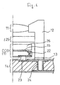
- FIG.6 is a fragmental detailed view of the lower view of FIG. 5, in which the through electrodes 22 are formed.
- 24 is a wiring portion of the printed-circuit board 14
- 125 is an IR-cut filter portion
- 26 is a transparent insulating layer.
- Patent Literature 1 Japanese Patent Unexamined Publication No. 2003-169235 (which is hereinafter referred as Patent Literature 1), as the conventional example of the camera module using CCD, the imaging device has been proposed for the purpose of reducing the number of articles of the module parts, achieving a reduction in size and weight, and reducing a production cost.
- the circuit board on which the cylindrical housing, the condensing lens fitted to the opening portion of the housing on one side to converge a light incident from the opening portion, and the sensor device fitted to the opening portion of the housing on the other side to receive the light converged by the condensing lens are mounted is fitted, and the circuit board and the housing are bonded at their boundaries.
- the sensor device and the circuit board are connected by using the bonding wires and thus there is a limit to a size reduction because a space portion into which the bonding wires are housed is needed.
- Patent Literature 2 Japanese Patent Unexamined Publication No. 2004-22990 (which is hereinafter referred as Patent Literature 2), as the conventional example in which the through electrodes are formed in the substrate, the through hole plugging method of forming the through holes in the silicon substrate and then filling the metal in the through holes by plugging using the plating has been proposed.
- this plugging method in order to improve a density and adhesiveness of the plug metal by removing the fine voids generated in the plug metal, the metal is filled in the through holes in the silicon substrate by the electroplating, then both surfaces of the silicon substrate are planarized, and then the high-pressure annealing process is applied to the silicon substrate.
- the present invention intends to reduce at least some of the above problems.
- the object is solved by the semiconductor device having a through electrode according to independent claim 1, and by the method of manufacturing a semiconductor device having a through electrode according to claim 1.
- a method of manufacturing a semiconductor device having a through electrode includes the steps of forming at least one through hole in a substrate; forming a first metal layer on one surface of the substrate and providing or forming an insulating protection film on the first metal layer; forming at least one through electrode by filling the at least one through hole with a second metal by virtue of an electroplating of the second metal applied from other or from another surface of the substrate while using the first metal layer as a power feeding layer; removing the insulating protection film; and removing the first metal layer located in an area or in areas other than peripheral portion(s) of the at least one through electrode.
- more than one through electrode is formed by forming more than one through hole.
- a further method of manufacturing a semiconductor device having a through electrode includes forming through holes in a substrate, forming a first metal layer from one surface side of the substrate and pasting a protection film on one surface of the substrate, forming through electrodes by filling the through holes with a second metal by means of an electroplating of the second metal applied from other or from another surface of the substrate while using the first metal layer as a power feeding layer, removing the protection film, and removing the first metal layer located in areas other than peripheral portions of the through electrodes.
- the substrate may be a semiconductor substrate. Further, a device layer and electrode pads may be formed on the one surface of the semiconductor substrate, and the through holes may be formed to pass through the electrode pads, a first insulating film provided under the electrode pads, and the substrate.
- first opening portions from which the first insulating film is exposed are optionally formed in the electrode pads by an etching and second opening portions from which the semiconductor substrate is exposed and areas of which are smaller than the first opening portions are optionally formed by applying an etching to the first insulating film exposed from the first opening portions, and then the through holes whose sectional areas are smaller than the second opening portions are formed by applying the etching to portions of the semiconductor substrate exposed from the second opening portions.
- a second insulating film is optionally formed on an overall surface of the substrate containing inner walls of the through holes.
- a resist is formed on one surface of the substrate other than peripheral portions of the through holes, then the second insulating film is formed on an overall surface of the substrate containing the inner walls of the through holes, then the resist and the second insulating film on the resist are removed, and then the first metal layer is formed.
- the second insulating film is formed on an overall surface of the substrate containing the inner walls of the through holes, then a resist is formed on peripheral portions of the through holes on one surface of the substrate, then the second insulating film not covered with the resist is removed by an etching, then the resist is removed, and then the first metal layer is formed.
- the first metal layer may be formed by a chromium and copper sputtering, and the second metal may be formed by a copper plating.
- a method of manufacturing a semiconductor device having a through electrode which includes the steps of forming a device layer on one surface of a semiconductor substrate and forming at least one electrode pad connected electrically to the device layer, preferably around the device layer or next to the device layer; forming at least one through hole to pass through the electrode pad(s); a first insulating film provided under the electrode pad(s), and the semiconductor substrate; covering an overall surface containing at least one inner wall surface of the through hole (s), the first insulating film, and at least one opening portion of the electrode pad(s) with a second insulating film; removing the second insulating film from at least a part of an area or of areas of an upper surface or of upper surfaces of the electrode pad(s); forming a first metal layer from one surface side of the semiconductor substrate to cover at least a periphery or peripheries of the at least one opening portion of the at least one through hole such that a part of the first metal layer is connected electrically to the electrode pad
- Both the device layer and the electrode pads may be formed on the first insulating film on the semiconductor substrate.
- the device layer may be formed directly on the semiconductor substrate, and the electrode pads may be formed on the first insulating film on the semiconductor substrate.
- the semiconductor device having a through electrode and the method of manufacturing the same may be advantageous in at least some of the following respects. They may be capable of achieving a cost reduction, a size reduction, an increase in density, and/or an increase in speed, for example by improving and simplifying the method of forming through electrodes in the silicon substrate, when devices such as a CCD (charge coupled device), a CMOS device, a memory device, and the like and module parts such as a camera module, a memory multi-stage module, and the like are manufactured.
- CCD charge coupled device
- CMOS device complementary metal oxide semiconductor device
- the invention is also directed to apparatuses for carrying out the disclosed methods and including apparatus parts for performing each described method steps. These method steps may be performed by way of hardware components, a computer programmed by appropriate software, by any combination of the two or in any other manner. Furthermore, the invention is also directed to methods by which the described apparatus operates. It includes method steps for carrying out every function of the apparatus or manufacturing every part of the apparatus.
- FIGS. 1 (a) to (d), FIGS.2(a) to (d), and FIGS.3(a) to (d) show a method of manufacturing a semiconductor device having a through electrode of the present invention in order of step.
- FIG.1(a) shows a semiconductor wafer (wiring substrate).
- an oxide film (SiO 2 film) 32 is formed as an insulating film that covers an upper surface of a silicon (Si) substrate (semiconductor substrate) 31.
- a device layer 33 such as a CCD or CMOS image sensor, a memory, or the like is formed on the oxide film 32.
- aluminumpads (electrode pads) 34 are formed around the device layer 33 on the oxide film 32 such that a part of them is overlapped with the device layer 33.
- an insulating film (passivating film) 35 is formed thereon over a whole surface.
- the passivating film 35 located on the aluminum pads 34 is removed from areas that are slightly narrower than areas of the aluminum pads 34 respectively to expose the aluminum pads 34.
- a GaAs semiconductor and the like other than the silicon substrate may be employed as the substrate 31.
- a thickness t of the silicon (Si) substrate 31 is set to 50 to 500 ⁇ m, for example, the aluminum pad 34 is shaped into a square a length a of one side of which is about 100 ⁇ m, for example, and a square area that is slightly narrower than the square is exposed from the passivating film 35.
- FIG.1(b) shows a state that the aluminum pads 34 exposed from the passivating film 35 are removed by the etching.
- a resist (not shown) is coated on the whole surface, and then this resist is patterned by the exposing/developing. Then, the etching is applied to an upper surface of the semiconductor wafer by using a dry (CI-based gas) or wet (phosphoric acid+acetic acid+hydrochloric acid) etchant or a Stanford etchant, which has no influence on the oxide film 32. Then, the resist is removed after the etching is finished.
- An opening portion 34a in the aluminum pad portion removed by such etching is a square a length b of one side of which is about 80 ⁇ m, for example, and thus the underlying oxide film 32 is exposed from the opening portion 34a.
- FIG.1 (c) shows a state that the oxide film 32 exposed from the opening portion 34a of the aluminum pads 34 is removed by the etching.
- a resist (not shown) is coated on the whole surface, and then this resist is patterned by the exposing/developing. Then, the etching is applied to an upper surface of the semiconductor wafer by using a dry (CHF 3 or CF 4 ) or wet (hydrofluoric acid) etchant, which has no influence on the silicon substrate 31. Then, the resist is removed after the etching is finished.
- a shape of the oxide film 32 removed by such etching is a square a length c of one side of which is about 60 ⁇ m, for example, and thus the upper surface of the silicon substrate 31 is exposed from the opening portion 32a of the oxide film 32 removed as a square.
- FIG.1 (d) shows a state that through holes 36 are formed in portions of the silicon substrate 31, which are exposed from the square opening portions 32a of the oxide film 32, by the hole opening process using the etching.
- a resist (not shown) is coated on the whole surface, and then this resist is patterned by the exposing/developing. Then, the etching is applied by using a dry (SF 6 gas) etchant. Then, the resist (not shown) is removed after the etching is finished.
- the hole opening process is applied to the silicon substrate 31 by the etching, such process is applied from the upper surface side of the semiconductor wafer on which the aluminum pads 34 are formed. But such process may be applied from the back surface of the silicon substrate 31.
- a resist (not shown) is coated on the back surface side of the silicon substrate 31, then this resist is patterned by the exposing/developing, and then an etchant is applied from the back surface side of the silicon substrate 31.
- the etching applied from the back surface side of the silicon substrate 31 is advantageous to the point of view that the device layer 33 is hardly affected by the plasma etching.
- the through holes 36 that pass through the silicon substrate 31 from the upper surface to the lower surface are formed in positions that correspond to the opening portions 32a of the oxide film 32.
- the through hole 36 has an inner diameter d of about 40 ⁇ m, for example.
- the inner wall of the through hole 36 has a stepwise section because of the different lengths b, c, d of the opening portions.
- this stepwise inner wall of the through hole 36 it is possible to extend the distance between side walls of the opening portions 34a of the electrode pads 34 and side walls of the opening portions of the silicon substrate 31. Therefore, it is possible to secure a sufficient insulation between the electrode pads 34 and the silicon substrate 31. Further, compared with the case where the inner walls of the through holes are not the stepwise shape, that is, the lengths of the opening portions are the same, vertically straight portions of the inner walls become short.
- FIG.2 (a) shows a state that resist patterns 37 are formed by coating a resist on the insulating film (passivating film) 35 and the aluminum pads 34 and then patterning this resist. More specifically, a resist is coated on the overall surface of the semiconductor wafer including the insulating film (passivating film) 35 and the aluminum pads 34, and then patterned by the exposing/developing such that the resist is removed from peripheral portions of the through holes including areas of the through holes 36 and the upper surface of the silicon substrate 31 around the through holes 36, exposed surfaces of the oxide film 32, and inner side portions of the aluminum pads 34.
- the resist patterns 37 for covering the whole surface of the passivating film 35 and a part of the aluminum pads 34 located adjacent to the passivating film 35 are formed.
- FIG.2(b) shows a state that a thin insulating film 38 is formed on the overall surface of the semiconductor wafer including the lower surface of the silicon substrate 31 and inner wall surfaces of the through holes 36.
- Such insulating film 38 can be formed by applying the low-temperature chemical vapor deposition (CVD) from the upper and lower surfaces of the semiconductor wafer at 250 °C, or less, for example. But the insulating film 38 may be formed on the overall surface of the semiconductor wafer by turning the semiconductor wafer upside down after CVD is applied from the upper surface of the semiconductor wafer, and then applying CVD from the lower surface.
- As the material of the insulating film 38 used in CVD SiOx, SiNx, SiNOx, or the like can be employed.
- a thickness of the insulating film 38 is set to about 0.2 to 0.5 ⁇ m, for example. Accordingly, the insulating film 38 is formed on the overall surface of the semiconductor wafer including the inner walls of the through holes 36.
- FIG.2 (c) shows a state that the resist patterns 37 formed in step in FIG.2 (a) are removed.
- the resist patterns 37 are removed and simultaneously the insulating film 38 on the upper surface of the resist patterns 37 is also removed.
- the aluminum pads 34 are exposed partially and also the passivating film 35 for covering the device layer 33 is exposed.
- the inner surface sides of the through holes 36 and the back surface side of the semiconductor wafer are still covered with the insulating film 38.
- steps in FIG.2(a) to FIG.2(c) can be replaced with following steps, for example. That is, in FIG.2(a), first the resist patterns 37 are formed on the passivating film 35 and the aluminum pads 34. In this case, prior to the formation of the resist layers 37, the insulating film 38 in the step of FIG.2 (b) is formed on the overall upper and lower surfaces of the semiconductor wafer including the inner wall surfaces of the through holes 36. Then, a resist (not shown) is coated on the insulating film 38 and is patterned.
- the semiconductor wafer similar to that shown in FIG.2(c) can be formed by the approach other than the lift-off method.
- FIG.2 (d) shows a state that a metal film 39 is formed from the upper side of the semiconductor wafer by the sputtering.
- a metal film 39 As the metal film 39, a chromium (Cr) film of 50 ⁇ m thickness, for example, is formed and a copper (Cu) film of 500 nm thickness, for example, is formed thereon. Since the metal film 39 is formed from the upper side of the semiconductor wafer by the sputtering, the overall upper surface of the semiconductor wafer is covered with the metal film 39 that is electrically conductive. In contrast, the metal film 39 is adhered onto only the inner walls of the through holes 36 on the upper portion of the semiconductor wafer, but the metal film 39 is never adhered onto most of the inner wall areas of the through holes 36 and the lower surface of the wafer.
- FIG.3(a) shows a state that a protection film 40 is pasted onto the upper surface of the wafer.
- a proper pressure e.g., 1 MPa
- a proper temperature e.g. 150 °C
- FIG.3 (b) shows a state that through electrodes 42 are formed by applying the electrolytic copper plating from the back surface of the wafer, while feeding an electroplating power from the end portions of the metal film 39 formed on the overall area of the upper surface of the wafer, as indicated with an arrow 41.
- the copper (Cu) electroplating can be applied by using the metal film 39 over the through holes 36 as one electrode.
- the insides of the through holes 36 are filled completely with the copper and the through electrodes 42 can be formed.
- the copper is never adhered onto the upper surface of the wafer, e.g., the metal film 39 existing on the passivating film 35, and the like by the electroplating.
- FIG. 3 (c) shows a state that the protection film 40 pasted onto the upper surface of the wafer is removed by the ultraviolet irradiation. This is because the metal film 39 used as the power feeding layer in the electroplating must be removed partially by subsequent step.
- FIG.3(d) shows a state that the metal film 39 is removed from the areas except the peripheral portions of the through holes 36.
- the etching of the copper (Cu) and chromium (Cr) is applied to remove partially the metal film 39 in this manner.
- a resist (not shown) is coated on the overall area of the upper surface of the wafer, and then this resist is patterned by the exposing/developing. Then, the etching is applied while using the dry or wet etchant of the Stanford etchant. Then, the resist is removed after the etching is completed.
- wirings may be formed on the passivating film 35 by etching the metal film to shape the wiring patterns.
- the semiconductor device (wiring substrate) having the through electrode of the present invention can be manufactured through respective steps in FIGS.1(a) to (d), FIGS.2(a) to (d), and FIGS.3(a) to (d).
- FIG.4 shows the case where the semiconductor device having rewirings on its back surface is formed by using the semiconductor device (wiring substrate) manufactured by above steps.
- Such semiconductor device can be manufactured by following steps, for example.
- the through electrodes 42 protruded from the bottom portions of the through holes 36 are planarized by polishing the back surface of the semiconductor wafer in a state of FIG.3 (d) . Then, a copper (Cu) /chromium (Cr) film is formed on the back surface of the wafer by the sputtering. Then, rewiring portions 50 are formed by coating a resist (not shown) and patterning the resist by means of the exposing/developing. Then, a resist 51 is coated, and this resist 51 is patterned to expose only the portions in which external connection terminals are formed.
- a nickel (Ni)/gold (Au) plating 53 is applied to the forming portions of the external connection terminal on the rewiring portions 50, and then solder bumps 52 acting as the external connection terminals are formed thereon.
- the dicing is applied to predetermined portions of the semiconductor wafer. In this manner, the semiconductor device having the rewirings on the back surface shown in FIG.4 is obtained.
- the present invention is explained with reference to the accompanying drawings. But the present invention is not limited to the above embodiment, and can be varied, modified, etc. into various modes within a spirit and a scope of the present invention.
- the through electrodes are formed in the semiconductor wafer and then the individual semiconductor devices are manufactured by cutting away the wafer by means of the dicing.
- the case where both the device layer 33 and the electrode (aluminum) pads 34 are formed on the first insulating film (oxide film 32) on the silicon substrate 31 is explained.
- the device layer 33 is formed directly on the silicon substrate 31 depending upon the devices such as the transistor, and the like.
- the first insulating film (oxide film 32) is formed below the electrode pads 34.
- the through electrodes can be formed in the silicon substrate in the devices such as a CCD (charge coupled device), a CMOS device, a memory device, and the like and the module parts such as a camera module, a memory multi-stage module, and the like by a simple method, and also a cost reduction, a size reduction, an increase in density, and an increase in speed can be achieved.
- CCD charge coupled device
- CMOS complementary metal-oxide-oxide
- the module parts such as a camera module, a memory multi-stage module, and the like by a simple method, and also a cost reduction, a size reduction, an increase in density, and an increase in speed can be achieved.
Landscapes
- Engineering & Computer Science (AREA)
- Manufacturing & Machinery (AREA)
- Microelectronics & Electronic Packaging (AREA)
- Internal Circuitry In Semiconductor Integrated Circuit Devices (AREA)
- Junction Field-Effect Transistors (AREA)
Abstract
Description
- The present disclosure relates to a semiconductor device, more specifically to a semiconductor device having a through electrode, and to a method of manufacturing the same. The present disclosure can be applied as a three-dimensional packaging method that is, for example, applied to form through electrodes in a silicon substrate, in devices such as a CCD (charge coupled device) for receiving light converged by a condensing lens, a CMOS device, a memory device and the like, and in module parts such as a camera module, a memory multi-stage module, and the like.
- With the rapid progress and development of the information communication technology, improvement in a data communication speed and increase of an amount of data communication can be realized recently. Among the mobile electronic devices such as the cellular phone, the notebook personal computer, and the like, the mobile electronic device into which the imaging device having the image pickup device such as the CCD image sensor, the CMOS image sensor, or the like is incorporated is spreading now. These devices can transmit the image data picked up by the imaging device in addition to the character data in real time.
- A sectional structure of the camera module (imaging device) in the related art is shown in FIG.5. An upper view shows the module of the type in which the image pickup device and the substrate are connected by the wire bonding. A
housing 12 having acondensing lens 11 in an opening portion at its one end is provided on a printed-circuit board 14 with an adhesive 13. In the inside of thehousing 12, an image pickup device 1 (CCD or CMOS image sensor) in which alight receiving portion 15 is formed on an upper surface of asilicon substrate 16 is mounted on the printed-circuit board 14 with an adhesive 17.Electrode pads 18 are formed in the peripheral area of thelight receiving portion 15 on the upper surface of thesilicon substrate 16. Theelectrode pads 18 andterminal pads 20 on the printed-circuit board 14 are connected electrically via abonding wire 19 respectively. Here, 21 denotes a passive element such as a chip capacitor, or the like, which is fixed to the printed-circuit board 14 on the outside of thehousing 12 with solder. - Since a light is converged by the
condensing lens 11 provided to one end of thehousing 12 and then received by thelight receiving portion 15 of theimage pickup device 1, the imaging function of the optical device such as the camera, or the like can be fulfilled. In the device of the type that theelectrode pads 18 provided to the peripheral area of the upper surface of thesilicon substrate 16 and theterminal pads 20 on the printed-circuit board 14 are connected via thebonding wires 19, as shown in the upper view of FIG. 5, such a problem existed that a size of the device is increased. - In a lower view of FIG.5, such a structure that through
electrodes 22 are formed in thesilicon substrate 16 is employed in place of the arrangement of the electrode pads on the periphery of the upper surface of thesilicon substrate 16 of theimage pickup device 1, and thus a size of the device can be decreased. More particularly, thethrough electrodes 22 are formed in the peripheral area of thesilicon substrate 16 to pass through vertically, and then upper ends of the throughelectrodes 22 are connected electrically to thelight receiving portion 15 and also lower ends of the throughelectrodes 22 are connected electrically to theterminal pads 20 viabumps 23. In this manner, theimage pickup device 1 on the upper surface of which thelight receiving portion 15 is formed is mounted on the printed-circuit board 14 by the flip-chip bonding, so that thelight receiving portion 15 and the printed-circuit board 14 are connected electrically mutually. Thus, a space portion into which thebonding wires 19 are housed can be omitted. Accordingly, a size of thehousing 12 can be reduced and also the camera module can be reduced in size as a whole from a size shown in the upper view of FIG.5 to a size shown in the lower view of the same, as indicated by abroken line 25. - FIG.6 is a fragmental detailed view of the lower view of FIG. 5, in which the
through electrodes 22 are formed. Here, 24 is a wiring portion of the printed-circuit board - In
Japanese Patent Unexamined Publication No. 2003-169235 Patent Literature 1, the sensor device and the circuit board are connected by using the bonding wires and thus there is a limit to a size reduction because a space portion into which the bonding wires are housed is needed. - Also, in
Japanese Patent Unexamined Publication No. 2004-22990 - As described above, in the device of the type that the image pickup device and the circuit board are connected by the wire bonding as shown in the upper view of FIG. 5 and
Patent Literature 1, there is a limit to the size reduction because the space portion into which the bonding wires are housed is needed. - The present invention intends to reduce at least some of the above problems. The object is solved by the semiconductor device having a through electrode according to
independent claim 1, and by the method of manufacturing a semiconductor device having a through electrode according toclaim 1. - Further advantages, features, aspects and details of the invention are evident from the dependent claims, the description and the drawings.
- An example implementation of the invention is described below. A method of manufacturing a semiconductor device having a through electrode includes the steps of forming at least one through hole in a substrate; forming a first metal layer on one surface of the substrate and providing or forming an insulating protection film on the first metal layer; forming at least one through electrode by filling the at least one through hole with a second metal by virtue of an electroplating of the second metal applied from other or from another surface of the substrate while using the first metal layer as a power feeding layer; removing the insulating protection film; and removing the first metal layer located in an area or in areas other than peripheral portion(s) of the at least one through electrode. Preferably, more than one through electrode is formed by forming more than one through hole.
- A further method of manufacturing a semiconductor device having a through electrode includes forming through holes in a substrate, forming a first metal layer from one surface side of the substrate and pasting a protection film on one surface of the substrate, forming through electrodes by filling the through holes with a second metal by means of an electroplating of the second metal applied from other or from another surface of the substrate while using the first metal layer as a power feeding layer, removing the protection film, and removing the first metal layer located in areas other than peripheral portions of the through electrodes.
- The substrate may be a semiconductor substrate. Further, a device layer and electrode pads may be formed on the one surface of the semiconductor substrate, and the through holes may be formed to pass through the electrode pads, a first insulating film provided under the electrode pads, and the substrate.
- Before the through holes are formed in the semiconductor substrate, first opening portions from which the first insulating film is exposed are optionally formed in the electrode pads by an etching and second opening portions from which the semiconductor substrate is exposed and areas of which are smaller than the first opening portions are optionally formed by applying an etching to the first insulating film exposed from the first opening portions, and then the through holes whose sectional areas are smaller than the second opening portions are formed by applying the etching to portions of the semiconductor substrate exposed from the second opening portions.
- After the through holes are formed in the substrate but before the first metal layer is formed on one surface of the substrate, a second insulating film is optionally formed on an overall surface of the substrate containing inner walls of the through holes.
- Optionally, a resist is formed on one surface of the substrate other than peripheral portions of the through holes, then the second insulating film is formed on an overall surface of the substrate containing the inner walls of the through holes, then the resist and the second insulating film on the resist are removed, and then the first metal layer is formed. Alternately the second insulating film is formed on an overall surface of the substrate containing the inner walls of the through holes, then a resist is formed on peripheral portions of the through holes on one surface of the substrate, then the second insulating film not covered with the resist is removed by an etching, then the resist is removed, and then the first metal layer is formed.
- The first metal layer may be formed by a chromium and copper sputtering, and the second metal may be formed by a copper plating.
- Also, according to the present invention, there is provided a method of manufacturing a semiconductor device having a through electrode, which includes the steps of forming a device layer on one surface of a semiconductor substrate and forming at least one electrode pad connected electrically to the device layer, preferably around the device layer or next to the device layer; forming at least one through hole to pass through the electrode pad(s); a first insulating film provided under the electrode pad(s), and the semiconductor substrate; covering an overall surface containing at least one inner wall surface of the through hole (s), the first insulating film, and at least one opening portion of the electrode pad(s) with a second insulating film; removing the second insulating film from at least a part of an area or of areas of an upper surface or of upper surfaces of the electrode pad(s); forming a first metal layer from one surface side of the semiconductor substrate to cover at least a periphery or peripheries of the at least one opening portion of the at least one through hole such that a part of the first metal layer is connected electrically to the electrode pad(s); pasting an insulating tape on the first metal layer; forming at least one through electrode by filling the through holes with a second metal by virtue of an electroplating of the second metal applied from other or from another surface of the semiconductor substrate while using the first metal layer as a power feeding layer; removing the insulating tape; and removing the first metal layer located in an area or in areas other than peripheral portion(s) of the at least one through electrode. Preferably, more than one electron is formed. Then, more than one electrode pad and more than one through hole etc. is formed.
- Both the device layer and the electrode pads may be formed on the first insulating film on the semiconductor substrate. Alternately, the device layer may be formed directly on the semiconductor substrate, and the electrode pads may be formed on the first insulating film on the semiconductor substrate.
- The semiconductor device having a through electrode and the method of manufacturing the same may be advantageous in at least some of the following respects. They may be capable of achieving a cost reduction, a size reduction, an increase in density, and/or an increase in speed, for example by improving and simplifying the method of forming through electrodes in the silicon substrate, when devices such as a CCD (charge coupled device), a CMOS device, a memory device, and the like and module parts such as a camera module, a memory multi-stage module, and the like are manufactured.
- The invention is also directed to apparatuses for carrying out the disclosed methods and including apparatus parts for performing each described method steps. These method steps may be performed by way of hardware components, a computer programmed by appropriate software, by any combination of the two or in any other manner. Furthermore, the invention is also directed to methods by which the described apparatus operates. It includes method steps for carrying out every function of the apparatus or manufacturing every part of the apparatus.
- The invention will be better understood by reference to the following description of embodiments of the invention taken in conjunction with the accompanying drawings, wherein:
- FIGS.1(a) to (d) are sectional views showing a method of manufacturing a semiconductor device having a through electrode according to an embodiment of the present invention in order of step.
- FIGS.2 (a) to (d) are sectional views showing the method of manufacturing the semiconductor device having the through electrode according to the embodiment of the present invention in order of step subsequently to FIG.1.
- FIG.3 (a) to (d) are sectional views showing the method of manufacturing the semiconductor device having the through electrode according to the embodiment of the present invention in order of step subsequently to FIG.2.
- FIG.4 is a sectional view showing the semiconductor device using the wiring substrate manufactured by the present invention.
- FIG.5 is a view showing a camera module having the through electrode manufactured in the related art.
- FIG.6 is a fragmental detailed view of a lower view of FIG.5.
- An embodiment of the present invention will be explained in detail with reference to FIG.1 to FIG.4 hereinafter. FIGS. 1 (a) to (d), FIGS.2(a) to (d), and FIGS.3(a) to (d) show a method of manufacturing a semiconductor device having a through electrode of the present invention in order of step.
- FIG.1(a) shows a semiconductor wafer (wiring substrate). In this semiconductor wafer, an oxide film (SiO2 film) 32 is formed as an insulating film that covers an upper surface of a silicon (Si) substrate (semiconductor substrate) 31. Then, a
device layer 33 such as a CCD or CMOS image sensor, a memory, or the like is formed on theoxide film 32. Then, aluminumpads (electrode pads) 34 are formed around thedevice layer 33 on theoxide film 32 such that a part of them is overlapped with thedevice layer 33. Then, an insulating film (passivating film) 35 is formed thereon over a whole surface. Then, only thepassivating film 35 located on thealuminum pads 34 is removed from areas that are slightly narrower than areas of thealuminum pads 34 respectively to expose thealuminum pads 34. In this case, a GaAs semiconductor and the like other than the silicon substrate may be employed as thesubstrate 31. - Here, by way of example, it is preferably that a thickness t of the silicon (Si)
substrate 31 is set to 50 to 500 µm, for example, thealuminum pad 34 is shaped into a square a length a of one side of which is about 100 µm, for example, and a square area that is slightly narrower than the square is exposed from thepassivating film 35. - FIG.1(b) shows a state that the
aluminum pads 34 exposed from thepassivating film 35 are removed by the etching. As the etching process in this case, for example, a resist (not shown) is coated on the whole surface, and then this resist is patterned by the exposing/developing. Then, the etching is applied to an upper surface of the semiconductor wafer by using a dry (CI-based gas) or wet (phosphoric acid+acetic acid+hydrochloric acid) etchant or a Stanford etchant, which has no influence on theoxide film 32. Then, the resist is removed after the etching is finished. Anopening portion 34a in the aluminum pad portion removed by such etching is a square a length b of one side of which is about 80 µm, for example, and thus theunderlying oxide film 32 is exposed from theopening portion 34a. - FIG.1 (c) shows a state that the
oxide film 32 exposed from theopening portion 34a of thealuminum pads 34 is removed by the etching. As the etching process in this case, for example, a resist (not shown) is coated on the whole surface, and then this resist is patterned by the exposing/developing. Then, the etching is applied to an upper surface of the semiconductor wafer by using a dry (CHF3 or CF4) or wet (hydrofluoric acid) etchant, which has no influence on thesilicon substrate 31. Then, the resist is removed after the etching is finished. A shape of theoxide film 32 removed by such etching is a square a length c of one side of which is about 60 µm, for example, and thus the upper surface of thesilicon substrate 31 is exposed from theopening portion 32a of theoxide film 32 removed as a square. - FIG.1 (d) shows a state that through
holes 36 are formed in portions of thesilicon substrate 31, which are exposed from the square openingportions 32a of theoxide film 32, by the hole opening process using the etching. As the etching process in this case, for example, a resist (not shown) is coated on the whole surface, and then this resist is patterned by the exposing/developing. Then, the etching is applied by using a dry (SF6 gas) etchant. Then, the resist (not shown) is removed after the etching is finished. - When the hole opening process is applied to the
silicon substrate 31 by the etching, such process is applied from the upper surface side of the semiconductor wafer on which thealuminum pads 34 are formed. But such process may be applied from the back surface of thesilicon substrate 31. In this case, a resist (not shown) is coated on the back surface side of thesilicon substrate 31, then this resist is patterned by the exposing/developing, and then an etchant is applied from the back surface side of thesilicon substrate 31. In this manner, the etching applied from the back surface side of thesilicon substrate 31 is advantageous to the point of view that thedevice layer 33 is hardly affected by the plasma etching. - According to such etching, the through
holes 36 that pass through thesilicon substrate 31 from the upper surface to the lower surface are formed in positions that correspond to the openingportions 32a of theoxide film 32. The throughhole 36 has an inner diameter d of about 40 µm, for example. - According to the above-mentioned structure, the inner wall of the through
hole 36 has a stepwise section because of the different lengths b, c, d of the opening portions. With this stepwise inner wall of the throughhole 36, it is possible to extend the distance between side walls of the openingportions 34a of theelectrode pads 34 and side walls of the opening portions of thesilicon substrate 31. Therefore, it is possible to secure a sufficient insulation between theelectrode pads 34 and thesilicon substrate 31. Further, compared with the case where the inner walls of the through holes are not the stepwise shape, that is, the lengths of the opening portions are the same, vertically straight portions of the inner walls become short. Therefore, in the case where aninsulation film 38 and ametal layer 39 which are mentioned later are formed by spattering or CVD, it is possible to form sequentially these film and layer with a sufficient thickness. Therefore, it is possible to secure the sufficient electrical connection and also the sufficient insulation. - FIG.2 (a) shows a state that resist
patterns 37 are formed by coating a resist on the insulating film (passivating film) 35 and thealuminum pads 34 and then patterning this resist. More specifically, a resist is coated on the overall surface of the semiconductor wafer including the insulating film (passivating film) 35 and thealuminum pads 34, and then patterned by the exposing/developing such that the resist is removed from peripheral portions of the through holes including areas of the throughholes 36 and the upper surface of thesilicon substrate 31 around the throughholes 36, exposed surfaces of theoxide film 32, and inner side portions of thealuminum pads 34. Thus, the resistpatterns 37 for covering the whole surface of thepassivating film 35 and a part of thealuminum pads 34 located adjacent to thepassivating film 35 are formed. - FIG.2(b) shows a state that a thin insulating
film 38 is formed on the overall surface of the semiconductor wafer including the lower surface of thesilicon substrate 31 and inner wall surfaces of the through holes 36. Such insulatingfilm 38 can be formed by applying the low-temperature chemical vapor deposition (CVD) from the upper and lower surfaces of the semiconductor wafer at 250 °C, or less, for example. But the insulatingfilm 38 may be formed on the overall surface of the semiconductor wafer by turning the semiconductor wafer upside down after CVD is applied from the upper surface of the semiconductor wafer, and then applying CVD from the lower surface. As the material of the insulatingfilm 38 used in CVD, SiOx, SiNx, SiNOx, or the like can be employed. A thickness of the insulatingfilm 38 is set to about 0.2 to 0.5 µm, for example. Accordingly, the insulatingfilm 38 is formed on the overall surface of the semiconductor wafer including the inner walls of the through holes 36. - FIG.2 (c) shows a state that the resist
patterns 37 formed in step in FIG.2 (a) are removed. In order to remove the resistpatterns 37, it is advantageous to use the so-called lift-off method. According to the lift-off method, the resistpatterns 37 are removed and simultaneously the insulatingfilm 38 on the upper surface of the resistpatterns 37 is also removed. As a result, thealuminum pads 34 are exposed partially and also thepassivating film 35 for covering thedevice layer 33 is exposed. The inner surface sides of the throughholes 36 and the back surface side of the semiconductor wafer are still covered with the insulatingfilm 38. - In this case, steps in FIG.2(a) to FIG.2(c) can be replaced with following steps, for example. That is, in FIG.2(a), first the resist
patterns 37 are formed on thepassivating film 35 and thealuminum pads 34. In this case, prior to the formation of the resistlayers 37, the insulatingfilm 38 in the step of FIG.2 (b) is formed on the overall upper and lower surfaces of the semiconductor wafer including the inner wall surfaces of the through holes 36. Then, a resist (not shown) is coated on the insulatingfilm 38 and is patterned. Then, the insulatingfilm 38 on thepassivating film 35 and the insulating film on thealuminum pads 34 except end portions on the throughholes 36 side are removed by etching the insulatingfilm 38 using the patterned resist as a mask. Then, the used resist is removed. According to such steps, the semiconductor wafer similar to that shown in FIG.2(c) can be formed by the approach other than the lift-off method. - FIG.2 (d) shows a state that a
metal film 39 is formed from the upper side of the semiconductor wafer by the sputtering. As themetal film 39, a chromium (Cr) film of 50 µm thickness, for example, is formed and a copper (Cu) film of 500 nm thickness, for example, is formed thereon. Since themetal film 39 is formed from the upper side of the semiconductor wafer by the sputtering, the overall upper surface of the semiconductor wafer is covered with themetal film 39 that is electrically conductive. In contrast, themetal film 39 is adhered onto only the inner walls of the throughholes 36 on the upper portion of the semiconductor wafer, but themetal film 39 is never adhered onto most of the inner wall areas of the throughholes 36 and the lower surface of the wafer. - FIG.3(a) shows a state that a
protection film 40 is pasted onto the upper surface of the wafer. A proper pressure (e.g., 1 MPa) is applied to the material made of an insulating resin, e.g., a UV release tape, or the like, at a proper temperature (e.g., 150 °C) by the thermal press. Thus, thisprotection film 40 is pasted onto the overall area of the upper surface of the wafer. - FIG.3 (b) shows a state that through
electrodes 42 are formed by applying the electrolytic copper plating from the back surface of the wafer, while feeding an electroplating power from the end portions of themetal film 39 formed on the overall area of the upper surface of the wafer, as indicated with anarrow 41. In this manner, since themetal film 39 is formed on the overall area of the upper surface of the wafer, the copper (Cu) electroplating can be applied by using themetal film 39 over the throughholes 36 as one electrode. Thus, the insides of the throughholes 36 are filled completely with the copper and the throughelectrodes 42 can be formed. In contrast, since the upper surface of the wafer is protected with theprotection film 40, the copper is never adhered onto the upper surface of the wafer, e.g., themetal film 39 existing on thepassivating film 35, and the like by the electroplating. - FIG. 3 (c) shows a state that the
protection film 40 pasted onto the upper surface of the wafer is removed by the ultraviolet irradiation. This is because themetal film 39 used as the power feeding layer in the electroplating must be removed partially by subsequent step. - FIG.3(d) shows a state that the
metal film 39 is removed from the areas except the peripheral portions of the through holes 36. The etching of the copper (Cu) and chromium (Cr) is applied to remove partially themetal film 39 in this manner. As this etching method, as well known, a resist (not shown) is coated on the overall area of the upper surface of the wafer, and then this resist is patterned by the exposing/developing. Then, the etching is applied while using the dry or wet etchant of the Stanford etchant. Then, the resist is removed after the etching is completed. As a result, the overall conduction on the upper surface of the wafer via themetal film 39 is cut off, and only the throughelectrodes 42 in the throughholes 36 and the terminal portions on the upper and lower surfaces of them still remain as the conduction portions. In this case, wirings may be formed on thepassivating film 35 by etching the metal film to shape the wiring patterns. - After this, individual semiconductor devices are obtained by applying the dicing to predetermined portions of the semiconductor wafer.
- As described above, the semiconductor device (wiring substrate) having the through electrode of the present invention can be manufactured through respective steps in FIGS.1(a) to (d), FIGS.2(a) to (d), and FIGS.3(a) to (d).
- FIG.4 shows the case where the semiconductor device having rewirings on its back surface is formed by using the semiconductor device (wiring substrate) manufactured by above steps. Such semiconductor device can be manufactured by following steps, for example.
- The through
electrodes 42 protruded from the bottom portions of the throughholes 36 are planarized by polishing the back surface of the semiconductor wafer in a state of FIG.3 (d) . Then, a copper (Cu) /chromium (Cr) film is formed on the back surface of the wafer by the sputtering. Then, rewiringportions 50 are formed by coating a resist (not shown) and patterning the resist by means of the exposing/developing. Then, a resist 51 is coated, and this resist 51 is patterned to expose only the portions in which external connection terminals are formed. Then, a nickel (Ni)/gold (Au) plating 53 is applied to the forming portions of the external connection terminal on therewiring portions 50, and then solder bumps 52 acting as the external connection terminals are formed thereon. In turn, the dicing is applied to predetermined portions of the semiconductor wafer. In this manner, the semiconductor device having the rewirings on the back surface shown in FIG.4 is obtained. - With the above, the embodiment the present invention is explained with reference to the accompanying drawings. But the present invention is not limited to the above embodiment, and can be varied, modified, etc. into various modes within a spirit and a scope of the present invention. In this case, in the actual steps of manufacturing the semiconductor device, the through electrodes are formed in the semiconductor wafer and then the individual semiconductor devices are manufactured by cutting away the wafer by means of the dicing.
- Also, in the above embodiment, the case where both the
device layer 33 and the electrode (aluminum)pads 34 are formed on the first insulating film (oxide film 32) on thesilicon substrate 31 is explained. However, in some cases thedevice layer 33 is formed directly on thesilicon substrate 31 depending upon the devices such as the transistor, and the like. In this case, the first insulating film (oxide film 32) is formed below theelectrode pads 34. - As described above, according to the present invention, the through electrodes can be formed in the silicon substrate in the devices such as a CCD (charge coupled device), a CMOS device, a memory device, and the like and the module parts such as a camera module, a memory multi-stage module, and the like by a simple method, and also a cost reduction, a size reduction, an increase in density, and an increase in speed can be achieved.
Claims (12)
- A method of manufacturing a semiconductor device having a through electrode (42), comprising the steps of:forming a through hole (36) in a substrate (31);forming a first metal layer (39) on one surface of the substrate and providing an insulating protection film (40) on the first metal layer;forming the through electrode (42) by filling the through hole (36) with a second metal by virtue of an electroplating of the second metal applied from another surface of the substrate (31) while using the first metal layer (39) as a power feeding layer;removing the insulating protection film (40); andremoving the first metal layer (39) located in an area other than a peripheral portion of the through electrode (42).
- Method of manufacturing a semiconductor device having a through electrode according to claim 1, further comprising a step of:forming a device layer (33) and a first insulating film (32) on the one surface of the substrate and forming an electrode pad (34) above the first insulating film (32) on the one surface of the substrate,wherein the substrate (31) is a semiconductor substrate, and the through hole (36) is formed to pass through the electrode pad (34), the first insulating film (32) provided under the electrode pad, and the substrate (31).
- A method of manufacturing a semiconductor device having a through electrode, according to claim 2, further comprising a step of:before forming the through hole (36) in the semiconductor substrate, forming a first opening (34a) portion from which the first insulating film (32) is exposed in the electrode pad (34) by an etching, and forming a second opening portion (32a) from which the semiconductor substrate (31) is exposed and an area of which is smaller than the first opening portion (34a) by applying an etching to the first insulating film (32) exposed from the first opening portion (34a),wherein the through hole (36) whose sectional area is smaller than the second opening portion (32a) is formed by applying the etching to a portion of the semiconductor substrate (31) exposed from the second opening portion (32a).
- A method of manufacturing a semiconductor device having a through electrode, according to any of the preceding claims, further comprising a step of:after forming the through hole (36) in the substrate but before forming the first metal layer (39) on the one surface of the substrate, forming a second insulating film (38) on an overall surface of the substrate containing an inner wall of the through hole (36).
- A method of manufacturing a semiconductor device having a through electrode, according to claim 4, further comprising steps of:before forming the second insulating film (38), forming a resist (37) on the one surface of the substrate other than a peripheral portion of the through hole (36); andremoving the resist and the second insulating film on the resist,wherein the first metal layer (39) is formed after the removing step.
- A method of manufacturing a semiconductor device having a through electrode, according to claim 4 or 5, further comprising steps of:after forming the second insulating film (38), forming a resist (37) on a peripheral portion of the through hole on the one surface of the substrate; andremoving the second insulating film not covered with the resist or the portion of the second insulating film (38) not covered with the resist by an etching and then removing the resist (37),wherein the first metal layer (39) is formed after the removing step.
- A method of manufacturing a semiconductor device having a through electrode, according to any of the preceding claims, wherein the first metal layer (39) is formed by a chromium and copper sputtering, and the second metal is formed by a copper plating.
- A method of manufacturing a semiconductor device having a through electrode (42), comprising the steps of:forming a device layer (33) on one surface of a semiconductor substrate (31) and forming an electrode pad (34) connected electrically to the device layer (33);forming a through hole (36) to pass through the electrode pad (34), through a first insulating film (32) provided under the electrode pad, and through the semiconductor substrate (31);covering an overall surface containing an inner wall surface of the through hole (36), the first insulating film (32) or an opening portion thereof, and an opening portion of the electrode pad (34a), with a second insulating film (38);removing the second insulating film (38) from at least a part of an area of an upper surface of the electrode pad;forming a first metal layer (39) from one surface side of the semiconductor substrate to cover at least a periphery of the opening portion of the through hole (36) such that a part of the first metal layer (39) is connected electrically to the electrode pad (34);pasting an insulating tape (40) on the first metal layer (39);forming a through electrode (42) by filling the through hole (36) with a second metal by virtue of an electroplating of the second metal applied from another surface of the semiconductor substrate (31) while using the first metal layer (39) as a power feeding layer;removing the insulating tape (40); andremoving the first metal layer (39) located in an area other than a peripheral portion of the through electrode (42).
- A method of manufacturing a semiconductor device having a through electrode, according to any of claims 2 to 8, wherein both the device layer (33) and the electrode pad (34) are formed on the first insulating film (32) on the semiconductor substrate.
- A method of manufacturing a semiconductor device having a through electrode, according to any of claims 2 to 8, wherein the device layer (33) is formed directly on the semiconductor substrate (31), and the electrode pad (34) is formed on the first insulating film (32) on the semiconductor substrate (31).
- A semiconductor device comprising:a semiconductor substrate (31);a device layer (33) formed on one surface of the semiconductor substrate;an electrode pad (34) formed on the one surface of the semiconductor substrate and electrically connected with the device layer (33);a first insulating film (32) under the electrode pad (34) on the one surface of the semiconductor substrate (31);a through hole (36) passing through the electrode pad (34), the first insulating film (32) and the semiconductor substrate (31), and having an inner wall with a stepwise section;a second insulating film (38) formed on another surface of the semiconductor substrate, the inner wall of the through hole (36) and a peripheral portion of the through hole on the one surface of the semiconductor substrate;a through electrode (42) formed in the through hole (36) covered by the second insulating film (38); anda metal layer (39) formed on the peripheral portion of the through hole (36) on the one surface of the semiconductor substrate and electrically connecting the electrode pad (34) to the through electrode (42).
- A semiconductor device having a through electrode according to claim 11, wherein the through hole (36) has a diameter smaller at a portion passing through the first insulating film (32) than a portion passing through the electrode pad (34), and smaller at a portion passing through the semiconductor substrate (31) than the portion passing through the first insulating film (32).
Applications Claiming Priority (1)
| Application Number | Priority Date | Filing Date | Title |
|---|---|---|---|
| JP2005178534A JP4698296B2 (en) | 2005-06-17 | 2005-06-17 | Manufacturing method of semiconductor device having through electrode |
Publications (1)
| Publication Number | Publication Date |
|---|---|
| EP1734576A1 true EP1734576A1 (en) | 2006-12-20 |
Family
ID=36940439
Family Applications (1)
| Application Number | Title | Priority Date | Filing Date |
|---|---|---|---|
| EP06012546A Withdrawn EP1734576A1 (en) | 2005-06-17 | 2006-06-19 | Semiconductor device having through electrode and method of manufacturing the same |
Country Status (6)
| Country | Link |
|---|---|
| US (1) | US7524753B2 (en) |
| EP (1) | EP1734576A1 (en) |
| JP (1) | JP4698296B2 (en) |
| KR (1) | KR20060132490A (en) |
| CN (1) | CN1881535A (en) |
| TW (1) | TW200707643A (en) |
Cited By (3)
| Publication number | Priority date | Publication date | Assignee | Title |
|---|---|---|---|---|
| DE102006060205B3 (en) * | 2006-12-18 | 2008-04-17 | Forschungszentrum Jülich GmbH | Substrate's e.g. wafer, plated-through hole and strip conductor producing method, involves producing plated-through hole and strip conductor simultaneously on one side of substrate by further deposition of metal |
| WO2010041165A1 (en) * | 2008-10-10 | 2010-04-15 | Nxp B.V. | Method of plating through wafer vias in a wafer for 3d packaging |
| DE102009005458A1 (en) * | 2009-01-21 | 2010-08-12 | Austriamicrosystems Ag | Semiconductor component with through-hole and method for its production |
Families Citing this family (21)
| Publication number | Priority date | Publication date | Assignee | Title |
|---|---|---|---|---|
| US7199439B2 (en) * | 2004-06-14 | 2007-04-03 | Micron Technology, Inc. | Microelectronic imagers and methods of packaging microelectronic imagers |
| US7083425B2 (en) | 2004-08-27 | 2006-08-01 | Micron Technology, Inc. | Slanted vias for electrical circuits on circuit boards and other substrates |
| US8278738B2 (en) * | 2005-02-17 | 2012-10-02 | Sharp Kabushiki Kaisha | Method of producing semiconductor device and semiconductor device |
| JP4552770B2 (en) * | 2005-06-21 | 2010-09-29 | パナソニック電工株式会社 | Method for forming through wiring on semiconductor substrate |
| JP4533283B2 (en) * | 2005-08-29 | 2010-09-01 | 新光電気工業株式会社 | Manufacturing method of semiconductor device |
| JP2008305938A (en) * | 2007-06-07 | 2008-12-18 | Toshiba Corp | Semiconductor device, and manufacturing method thereof |
| JP5248084B2 (en) | 2007-10-26 | 2013-07-31 | 新光電気工業株式会社 | Silicon interposer, package for semiconductor device using the same, and semiconductor device |
| JP5311609B2 (en) | 2007-10-30 | 2013-10-09 | 新光電気工業株式会社 | Silicon interposer manufacturing method, silicon interposer, semiconductor device package and semiconductor device using the same |
| JP2009224492A (en) * | 2008-03-14 | 2009-10-01 | Oki Semiconductor Co Ltd | Semiconductor device and method of manufacturing the same |
| TWI389291B (en) * | 2008-05-13 | 2013-03-11 | 財團法人工業技術研究院 | Three-dimensional stacked die package structure |
| US7928534B2 (en) * | 2008-10-09 | 2011-04-19 | Taiwan Semiconductor Manufacturing Company, Ltd. | Bond pad connection to redistribution lines having tapered profiles |
| US8030780B2 (en) | 2008-10-16 | 2011-10-04 | Micron Technology, Inc. | Semiconductor substrates with unitary vias and via terminals, and associated systems and methods |
| US8736050B2 (en) | 2009-09-03 | 2014-05-27 | Taiwan Semiconductor Manufacturing Company, Ltd. | Front side copper post joint structure for temporary bond in TSV application |
| US8399354B2 (en) | 2009-01-13 | 2013-03-19 | Taiwan Semiconductor Manufacturing Company, Ltd. | Through-silicon via with low-K dielectric liner |
| JP5367616B2 (en) * | 2009-02-23 | 2013-12-11 | 新光電気工業株式会社 | Wiring board and manufacturing method thereof |
| JP4833307B2 (en) * | 2009-02-24 | 2011-12-07 | インターナショナル・ビジネス・マシーンズ・コーポレーション | Semiconductor module, terminal plate, method for manufacturing terminal plate, and method for manufacturing semiconductor module |
| US8759949B2 (en) * | 2009-04-30 | 2014-06-24 | Taiwan Semiconductor Manufacturing Company, Ltd. | Wafer backside structures having copper pillars |
| US8754507B2 (en) * | 2011-01-18 | 2014-06-17 | Hong Kong Applied Science and Technology Research Institute Company Limited | Forming through-silicon-vias for multi-wafer integrated circuits |
| JP6033130B2 (en) * | 2013-03-13 | 2016-11-30 | 新光電気工業株式会社 | Probe guide plate and manufacturing method thereof |
| KR102222485B1 (en) * | 2014-09-18 | 2021-03-04 | 에스케이하이닉스 주식회사 | Semiconductor device having through via, semiconductor package including the same and the method for manufacturing semiconductor device |
| KR102039887B1 (en) * | 2017-12-13 | 2019-12-05 | 엘비세미콘 주식회사 | Methods of fabricating semiconductor package using both side plating |
Citations (3)
| Publication number | Priority date | Publication date | Assignee | Title |
|---|---|---|---|---|
| US6039889A (en) * | 1999-01-12 | 2000-03-21 | Fujitsu Limited | Process flows for formation of fine structure layer pairs on flexible films |
| EP1267402A2 (en) * | 2001-06-14 | 2002-12-18 | Shinko Electric Industries Co. Ltd. | Semiconductor device and method of production of same |
| DE10244077A1 (en) * | 2002-09-06 | 2004-03-11 | INSTITUT FüR MIKROTECHNIK MAINZ GMBH | Production of a semiconductor component used in microelectronics comprises dry etching a hole in the substrate of a component, lining the hole with an insulating layer, removing the insulating layer, and producing an electrical connection |
Family Cites Families (14)
| Publication number | Priority date | Publication date | Assignee | Title |
|---|---|---|---|---|
| US5933712A (en) * | 1997-03-19 | 1999-08-03 | The Regents Of The University Of California | Attachment method for stacked integrated circuit (IC) chips |
| JP4296609B2 (en) * | 1998-04-10 | 2009-07-15 | 凸版印刷株式会社 | Manufacturing method of semiconductor inspection jig |
| US6114098A (en) * | 1998-09-17 | 2000-09-05 | International Business Machines Corporation | Method of filling an aperture in a substrate |
| JP3918350B2 (en) * | 1999-03-05 | 2007-05-23 | セイコーエプソン株式会社 | Manufacturing method of semiconductor device |
| US6495912B1 (en) * | 2001-09-17 | 2002-12-17 | Megic Corporation | Structure of ceramic package with integrated passive devices |
| JP4017382B2 (en) | 2001-11-30 | 2007-12-05 | 新光電気工業株式会社 | Imaging device |
| JP2003318178A (en) * | 2002-04-24 | 2003-11-07 | Seiko Epson Corp | Semiconductor device and its manufacturing method, circuit board, and electronic equipment |
| JP3910493B2 (en) * | 2002-06-14 | 2007-04-25 | 新光電気工業株式会社 | Semiconductor device and manufacturing method thereof |
| JP3904484B2 (en) | 2002-06-19 | 2007-04-11 | 新光電気工業株式会社 | Through-hole plugging method of silicon substrate |
| JP2004146742A (en) * | 2002-10-28 | 2004-05-20 | Shinko Electric Ind Co Ltd | Manufacturing method of wiring board |
| JP4213478B2 (en) | 2003-01-14 | 2009-01-21 | 株式会社ルネサステクノロジ | Manufacturing method of semiconductor device |
| TWI239629B (en) * | 2003-03-17 | 2005-09-11 | Seiko Epson Corp | Method of manufacturing semiconductor device, semiconductor device, circuit substrate and electronic apparatus |
| JP2004327910A (en) * | 2003-04-28 | 2004-11-18 | Sharp Corp | Semiconductor device and method of manufacturing the same |
| JP3891292B2 (en) * | 2003-05-19 | 2007-03-14 | セイコーエプソン株式会社 | Semiconductor device and manufacturing method thereof, circuit board, and electronic apparatus |
-
2005
- 2005-06-17 JP JP2005178534A patent/JP4698296B2/en not_active Expired - Fee Related
-
2006
- 2006-06-15 US US11/424,385 patent/US7524753B2/en active Active
- 2006-06-16 CN CNA200610086505XA patent/CN1881535A/en active Pending
- 2006-06-16 TW TW095121568A patent/TW200707643A/en unknown
- 2006-06-16 KR KR1020060054365A patent/KR20060132490A/en not_active Withdrawn
- 2006-06-19 EP EP06012546A patent/EP1734576A1/en not_active Withdrawn
Patent Citations (3)
| Publication number | Priority date | Publication date | Assignee | Title |
|---|---|---|---|---|
| US6039889A (en) * | 1999-01-12 | 2000-03-21 | Fujitsu Limited | Process flows for formation of fine structure layer pairs on flexible films |
| EP1267402A2 (en) * | 2001-06-14 | 2002-12-18 | Shinko Electric Industries Co. Ltd. | Semiconductor device and method of production of same |
| DE10244077A1 (en) * | 2002-09-06 | 2004-03-11 | INSTITUT FüR MIKROTECHNIK MAINZ GMBH | Production of a semiconductor component used in microelectronics comprises dry etching a hole in the substrate of a component, lining the hole with an insulating layer, removing the insulating layer, and producing an electrical connection |
Cited By (4)
| Publication number | Priority date | Publication date | Assignee | Title |
|---|---|---|---|---|
| DE102006060205B3 (en) * | 2006-12-18 | 2008-04-17 | Forschungszentrum Jülich GmbH | Substrate's e.g. wafer, plated-through hole and strip conductor producing method, involves producing plated-through hole and strip conductor simultaneously on one side of substrate by further deposition of metal |
| WO2010041165A1 (en) * | 2008-10-10 | 2010-04-15 | Nxp B.V. | Method of plating through wafer vias in a wafer for 3d packaging |
| DE102009005458A1 (en) * | 2009-01-21 | 2010-08-12 | Austriamicrosystems Ag | Semiconductor component with through-hole and method for its production |
| DE102009005458B4 (en) * | 2009-01-21 | 2010-09-30 | Austriamicrosystems Ag | Semiconductor component with through-hole and method for its production |
Also Published As
| Publication number | Publication date |
|---|---|
| TW200707643A (en) | 2007-02-16 |
| JP2006351968A (en) | 2006-12-28 |
| US20060286789A1 (en) | 2006-12-21 |
| JP4698296B2 (en) | 2011-06-08 |
| US7524753B2 (en) | 2009-04-28 |
| KR20060132490A (en) | 2006-12-21 |
| CN1881535A (en) | 2006-12-20 |
Similar Documents
| Publication | Publication Date | Title |
|---|---|---|
| US7524753B2 (en) | Semiconductor device having through electrode and method of manufacturing the same | |
| US7981727B2 (en) | Electronic device wafer level scale packages and fabrication methods thereof | |
| US7312521B2 (en) | Semiconductor device with holding member | |
| CN100576554C (en) | Image sensor package and manufacturing method thereof | |
| US6642615B2 (en) | Semiconductor device and method of manufacturing the same, circuit board and electronic instrument | |
| US8232202B2 (en) | Image sensor package and fabrication method thereof | |
| TWI382477B (en) | Wafer level package of electronic component and manufacturing method thereof | |
| TWI234261B (en) | Method of forming wafer backside interconnects | |
| CN100524725C (en) | Semiconductor device and manufacturing method of the same | |
| JP2007173483A (en) | Semiconductor device, method for manufacturing the same, and camera module | |
| EP1478021B1 (en) | Semiconductor device and manufacturing method thereof | |
| US20050161756A1 (en) | Package of a semiconductor device with a flexible wiring substrate and method for the same | |
| US7651886B2 (en) | Semiconductor device and manufacturing process thereof | |
| CN101950729B (en) | Wafer-level packaging of electronic components and manufacturing method thereof | |
| CN101355039B (en) | Image sensing element package and manufacturing method thereof | |
| CN101383299B (en) | Wafer-level packaging of electronic components and manufacturing method thereof | |
| JP2010016395A (en) | Manufacturing method for semiconductor device | |
| JP2004006835A (en) | Semiconductor device and manufacturing method thereof | |
| US6734042B2 (en) | Semiconductor device and method for fabricating the same | |
| JP4401330B2 (en) | Semiconductor device and manufacturing method thereof | |
| CN101383300B (en) | Wafer level package for electronic components and method of manufacturing the same | |
| JP2004006820A (en) | Semiconductor device and manufacturing method thereof | |
| CN1753163A (en) | Method for making connecting wires in backside of chip |
Legal Events
| Date | Code | Title | Description |
|---|---|---|---|
| PUAI | Public reference made under article 153(3) epc to a published international application that has entered the european phase |
Free format text: ORIGINAL CODE: 0009012 |
|
| AK | Designated contracting states |
Kind code of ref document: A1 Designated state(s): AT BE BG CH CY CZ DE DK EE ES FI FR GB GR HU IE IS IT LI LT LU LV MC NL PL PT RO SE SI SK TR |
|
| AX | Request for extension of the european patent |
Extension state: AL BA HR MK YU |
|
| 17P | Request for examination filed |
Effective date: 20070221 |
|
| AKX | Designation fees paid |
Designated state(s): DE FR |
|
| 17Q | First examination report despatched |
Effective date: 20120105 |
|
| STAA | Information on the status of an ep patent application or granted ep patent |
Free format text: STATUS: THE APPLICATION HAS BEEN WITHDRAWN |
|
| 18W | Application withdrawn |
Effective date: 20120425 |