EP1734498A1 - Plasma display apparatus - Google Patents
Plasma display apparatus Download PDFInfo
- Publication number
- EP1734498A1 EP1734498A1 EP06253103A EP06253103A EP1734498A1 EP 1734498 A1 EP1734498 A1 EP 1734498A1 EP 06253103 A EP06253103 A EP 06253103A EP 06253103 A EP06253103 A EP 06253103A EP 1734498 A1 EP1734498 A1 EP 1734498A1
- Authority
- EP
- European Patent Office
- Prior art keywords
- plasma display
- energy
- supply
- voltage
- sustain
- Prior art date
- Legal status (The legal status is an assumption and is not a legal conclusion. Google has not performed a legal analysis and makes no representation as to the accuracy of the status listed.)
- Withdrawn
Links
- 238000011084 recovery Methods 0.000 claims abstract description 113
- 239000003990 capacitor Substances 0.000 claims description 22
- 238000012423 maintenance Methods 0.000 description 10
- 230000006378 damage Effects 0.000 description 7
- 230000004888 barrier function Effects 0.000 description 5
- 230000003685 thermal hair damage Effects 0.000 description 5
- 230000007423 decrease Effects 0.000 description 4
- 239000011521 glass Substances 0.000 description 4
- 230000000630 rising effect Effects 0.000 description 4
- 239000000758 substrate Substances 0.000 description 4
- 239000010410 layer Substances 0.000 description 3
- 238000000034 method Methods 0.000 description 3
- 230000005855 radiation Effects 0.000 description 3
- 230000001186 cumulative effect Effects 0.000 description 2
- 239000007789 gas Substances 0.000 description 2
- 239000011261 inert gas Substances 0.000 description 2
- 229910052734 helium Inorganic materials 0.000 description 1
- 239000001307 helium Substances 0.000 description 1
- SWQJXJOGLNCZEY-UHFFFAOYSA-N helium atom Chemical compound [He] SWQJXJOGLNCZEY-UHFFFAOYSA-N 0.000 description 1
- AMGQUBHHOARCQH-UHFFFAOYSA-N indium;oxotin Chemical compound [In].[Sn]=O AMGQUBHHOARCQH-UHFFFAOYSA-N 0.000 description 1
- 238000009413 insulation Methods 0.000 description 1
- 239000000463 material Substances 0.000 description 1
- 239000007769 metal material Substances 0.000 description 1
- 239000000203 mixture Substances 0.000 description 1
- 238000012986 modification Methods 0.000 description 1
- 230000004048 modification Effects 0.000 description 1
- 229910052754 neon Inorganic materials 0.000 description 1
- GKAOGPIIYCISHV-UHFFFAOYSA-N neon atom Chemical compound [Ne] GKAOGPIIYCISHV-UHFFFAOYSA-N 0.000 description 1
- 239000011241 protective layer Substances 0.000 description 1
- 230000001360 synchronised effect Effects 0.000 description 1
- 229910052724 xenon Inorganic materials 0.000 description 1
- FHNFHKCVQCLJFQ-UHFFFAOYSA-N xenon atom Chemical compound [Xe] FHNFHKCVQCLJFQ-UHFFFAOYSA-N 0.000 description 1
Images




Classifications
-
- G—PHYSICS
- G09—EDUCATION; CRYPTOGRAPHY; DISPLAY; ADVERTISING; SEALS
- G09G—ARRANGEMENTS OR CIRCUITS FOR CONTROL OF INDICATING DEVICES USING STATIC MEANS TO PRESENT VARIABLE INFORMATION
- G09G3/00—Control arrangements or circuits, of interest only in connection with visual indicators other than cathode-ray tubes
- G09G3/20—Control arrangements or circuits, of interest only in connection with visual indicators other than cathode-ray tubes for presentation of an assembly of a number of characters, e.g. a page, by composing the assembly by combination of individual elements arranged in a matrix no fixed position being assigned to or needed to be assigned to the individual characters or partial characters
- G09G3/22—Control arrangements or circuits, of interest only in connection with visual indicators other than cathode-ray tubes for presentation of an assembly of a number of characters, e.g. a page, by composing the assembly by combination of individual elements arranged in a matrix no fixed position being assigned to or needed to be assigned to the individual characters or partial characters using controlled light sources
- G09G3/28—Control arrangements or circuits, of interest only in connection with visual indicators other than cathode-ray tubes for presentation of an assembly of a number of characters, e.g. a page, by composing the assembly by combination of individual elements arranged in a matrix no fixed position being assigned to or needed to be assigned to the individual characters or partial characters using controlled light sources using luminous gas-discharge panels, e.g. plasma panels
- G09G3/288—Control arrangements or circuits, of interest only in connection with visual indicators other than cathode-ray tubes for presentation of an assembly of a number of characters, e.g. a page, by composing the assembly by combination of individual elements arranged in a matrix no fixed position being assigned to or needed to be assigned to the individual characters or partial characters using controlled light sources using luminous gas-discharge panels, e.g. plasma panels using AC panels
- G09G3/296—Driving circuits for producing the waveforms applied to the driving electrodes
-
- G—PHYSICS
- G09—EDUCATION; CRYPTOGRAPHY; DISPLAY; ADVERTISING; SEALS
- G09G—ARRANGEMENTS OR CIRCUITS FOR CONTROL OF INDICATING DEVICES USING STATIC MEANS TO PRESENT VARIABLE INFORMATION
- G09G3/00—Control arrangements or circuits, of interest only in connection with visual indicators other than cathode-ray tubes
- G09G3/20—Control arrangements or circuits, of interest only in connection with visual indicators other than cathode-ray tubes for presentation of an assembly of a number of characters, e.g. a page, by composing the assembly by combination of individual elements arranged in a matrix no fixed position being assigned to or needed to be assigned to the individual characters or partial characters
- G09G3/22—Control arrangements or circuits, of interest only in connection with visual indicators other than cathode-ray tubes for presentation of an assembly of a number of characters, e.g. a page, by composing the assembly by combination of individual elements arranged in a matrix no fixed position being assigned to or needed to be assigned to the individual characters or partial characters using controlled light sources
- G09G3/28—Control arrangements or circuits, of interest only in connection with visual indicators other than cathode-ray tubes for presentation of an assembly of a number of characters, e.g. a page, by composing the assembly by combination of individual elements arranged in a matrix no fixed position being assigned to or needed to be assigned to the individual characters or partial characters using controlled light sources using luminous gas-discharge panels, e.g. plasma panels
- G09G3/288—Control arrangements or circuits, of interest only in connection with visual indicators other than cathode-ray tubes for presentation of an assembly of a number of characters, e.g. a page, by composing the assembly by combination of individual elements arranged in a matrix no fixed position being assigned to or needed to be assigned to the individual characters or partial characters using controlled light sources using luminous gas-discharge panels, e.g. plasma panels using AC panels
- G09G3/296—Driving circuits for producing the waveforms applied to the driving electrodes
- G09G3/2965—Driving circuits for producing the waveforms applied to the driving electrodes using inductors for energy recovery
-
- G—PHYSICS
- G09—EDUCATION; CRYPTOGRAPHY; DISPLAY; ADVERTISING; SEALS
- G09G—ARRANGEMENTS OR CIRCUITS FOR CONTROL OF INDICATING DEVICES USING STATIC MEANS TO PRESENT VARIABLE INFORMATION
- G09G2310/00—Command of the display device
- G09G2310/02—Addressing, scanning or driving the display screen or processing steps related thereto
- G09G2310/0202—Addressing of scan or signal lines
- G09G2310/0218—Addressing of scan or signal lines with collection of electrodes in groups for n-dimensional addressing
-
- G—PHYSICS
- G09—EDUCATION; CRYPTOGRAPHY; DISPLAY; ADVERTISING; SEALS
- G09G—ARRANGEMENTS OR CIRCUITS FOR CONTROL OF INDICATING DEVICES USING STATIC MEANS TO PRESENT VARIABLE INFORMATION
- G09G2330/00—Aspects of power supply; Aspects of display protection and defect management
- G09G2330/04—Display protection
-
- G—PHYSICS
- G09—EDUCATION; CRYPTOGRAPHY; DISPLAY; ADVERTISING; SEALS
- G09G—ARRANGEMENTS OR CIRCUITS FOR CONTROL OF INDICATING DEVICES USING STATIC MEANS TO PRESENT VARIABLE INFORMATION
- G09G2330/00—Aspects of power supply; Aspects of display protection and defect management
- G09G2330/04—Display protection
- G09G2330/045—Protection against panel overheating
-
- G—PHYSICS
- G09—EDUCATION; CRYPTOGRAPHY; DISPLAY; ADVERTISING; SEALS
- G09G—ARRANGEMENTS OR CIRCUITS FOR CONTROL OF INDICATING DEVICES USING STATIC MEANS TO PRESENT VARIABLE INFORMATION
- G09G3/00—Control arrangements or circuits, of interest only in connection with visual indicators other than cathode-ray tubes
- G09G3/20—Control arrangements or circuits, of interest only in connection with visual indicators other than cathode-ray tubes for presentation of an assembly of a number of characters, e.g. a page, by composing the assembly by combination of individual elements arranged in a matrix no fixed position being assigned to or needed to be assigned to the individual characters or partial characters
- G09G3/22—Control arrangements or circuits, of interest only in connection with visual indicators other than cathode-ray tubes for presentation of an assembly of a number of characters, e.g. a page, by composing the assembly by combination of individual elements arranged in a matrix no fixed position being assigned to or needed to be assigned to the individual characters or partial characters using controlled light sources
- G09G3/28—Control arrangements or circuits, of interest only in connection with visual indicators other than cathode-ray tubes for presentation of an assembly of a number of characters, e.g. a page, by composing the assembly by combination of individual elements arranged in a matrix no fixed position being assigned to or needed to be assigned to the individual characters or partial characters using controlled light sources using luminous gas-discharge panels, e.g. plasma panels
- G09G3/288—Control arrangements or circuits, of interest only in connection with visual indicators other than cathode-ray tubes for presentation of an assembly of a number of characters, e.g. a page, by composing the assembly by combination of individual elements arranged in a matrix no fixed position being assigned to or needed to be assigned to the individual characters or partial characters using controlled light sources using luminous gas-discharge panels, e.g. plasma panels using AC panels
- G09G3/291—Control arrangements or circuits, of interest only in connection with visual indicators other than cathode-ray tubes for presentation of an assembly of a number of characters, e.g. a page, by composing the assembly by combination of individual elements arranged in a matrix no fixed position being assigned to or needed to be assigned to the individual characters or partial characters using controlled light sources using luminous gas-discharge panels, e.g. plasma panels using AC panels controlling the gas discharge to control a cell condition, e.g. by means of specific pulse shapes
- G09G3/294—Control arrangements or circuits, of interest only in connection with visual indicators other than cathode-ray tubes for presentation of an assembly of a number of characters, e.g. a page, by composing the assembly by combination of individual elements arranged in a matrix no fixed position being assigned to or needed to be assigned to the individual characters or partial characters using controlled light sources using luminous gas-discharge panels, e.g. plasma panels using AC panels controlling the gas discharge to control a cell condition, e.g. by means of specific pulse shapes for lighting or sustain discharge
Definitions
- This document relates to a display apparatus. It more particularly relates to a plasma display apparatus.
- a plasma display apparatus is a type of display apparatus which comprises a plasma display panel and a driver for driving the plasma display panel.
- the plasma display panel comprises a front panel, a rear panel, and barrier ribs formed between the front panel and the rear panel.
- the barrier ribs form discharge cells.
- Each of the discharge cells is filled with an inert gas containing a main discharge gas such as neon (Ne), helium (He) or a Ne-He gas mixture and a small amount of xenon (Xe).
- a main discharge gas such as neon (Ne), helium (He) or a Ne-He gas mixture and a small amount of xenon (Xe).
- the inert gas within the discharge cells When a high frequency voltage generates a discharge, the inert gas within the discharge cells generates vacuum ultraviolet radiation.
- the vacuum ultraviolet radiation excites phosphors formed between the barrier ribs to emit visible light such that an image is displayed. Since the above-described type of plasma display panel can be manufactured to be thin and light, the plasma display panel has been considered as a next generation display apparatus.
- FIG. 1 illustrates a prior art driving apparatus of a prior art plasma display panel.
- a prior art driving apparatus of a plasma display panel comprises a sustain circuit unit 100, a setup supply unit 110, a negative polarity scan voltage supply unit 120, a set-down supply unit 130, a scan reference voltage supply unit 140, a drive integrated circuit (IC) 150, a seventh switch Q7 connected between the setup supply unit 110 and the drive IC 150, and a sixth switch Q6 connected between the sustain circuit unit 100 and the setup supply unit 110.
- IC drive integrated circuit
- the drive IC 150 is connected in a push-pull configuration.
- the drive IC 150 comprises a twelfth switch Q12 and a thirteenth switch Q13 for receiving a voltage signal from the sustain circuit unit 100, the setup supply unit 110, the negative polarity scan voltage supply unit 120, the set-down supply unit 130, and the scan reference voltage supply unit 140.
- An output line between the twelfth switch Q12 and the thirteenth switch Q13 is connected to one of plurality of scan electrodes of the plasma display panel Cp.
- the sustain circuit unit 100 recovers energy from the panel Cp and supplies a sustain voltage Vs to the panel Cp.
- the negative polarity scan voltage supply unit 120 supplies a scan pulse having a voltage magnitude of-Vy to the scan electrodes in an address period.
- the scan reference voltage supply unit 140 supplies a scan reference voltage Vsc to the scan electrodes in the address period.
- the set-down supply unit 130 supplies a falling ramp pulse to the scan electrodes in a set-down period of a reset period.
- the setup supply unit 110 supplies a rising ramp pulse to the scan electrodes in a setup period of the reset period.
- the plurality of sustain circuit units 100 are formed on a single board. This will be described with reference to FIG. 2.
- FIG. 2 illustrates an example of integrating a plurality of sustain circuit units into one module in a prior art driving apparatus of a plasma display panel.
- a plurality of sustain circuit units 200, 201 and 202 are formed on a single board.
- the plurality of sustain circuit units 200, 201 and 202 formed on the single board are commonly connected to a node n1.
- a reason for forming the plurality of sustain circuit units 200, 201 and 202 on the single board is that a sustain voltage Vs, which the sustain circuit units 200, 201 and 202 supply to a plasma display panel, is relatively high.
- the sustain circuit unit 200 when only the sustain circuit unit 200 supplies all of the sustain voltage Vs, electrical components, for example, an energy storing capacitor C1, a first switch Q1, a second switch Q2, a third switch Q3, a fourth switch Q4, a first diode D1, a second diode D2 and a first inductor L1 of the sustain circuit unit 200 must have a high withstanding voltage characteristic. Consequently, the fabricating cost of the driving apparatus increases.
- the forming of the plurality of sustain circuit units 200, 201 and 202 on the single board decreases the generation of heat and conduction resistance (Rds) in electrical components of each of the sustain circuit units 200, 201 and 202.
- the electrical components having an equal function need to have equal driving characteristics.
- variations in the fabricating processes of the electrical components cause differences between the driving characteristics of the electrical components.
- the sustain circuit unit 200 supplies the sustain voltage Vs at a time point t0
- the sustain circuit unit 201 supplies the sustain voltage Vs at a time point t1 later than the time point t0 by ⁇ t
- the sustain circuit unit 202 supplies the sustain voltage Vs at a time point t2 later than the time point t1 by ⁇ t.
- the sustain circuit unit 200 supplies the sustain voltage Vs more rapidly than the sustain circuit units 201 and 202.
- the present invention seeks to provide an improved plasma display apparatus.
- Embodiments of the present invention can provide a plasma display apparatus capable of preventing the excessive generation of heat and damage caused by a differences between driving characteristics in a sustain circuit unit.
- a plasma display apparatus comprises a plasma display panel comprising an electrode, a sustain voltage circuit unit comprising a plurality of sustain voltage circuits, arranged to maintain a voltage of the plasma display panel at a predetermined voltage and comprising a common input terminal, and an energy supply/recovery circuit unit comprising a plurality of energy supply/recovery circuits arranged to supply and recover energy to and from the plasma display panel, the plurality of energy supply/recovery circuits comprising a common output terminal and being connected to the sustain voltage circuit unit.
- the common output terminal of the energy supply/recovery circuit unit and the common input terminal of the sustain voltage circuit unit may be commonly connected to each other.
- the plurality of sustain voltage circuits may comprise a common output terminal.
- the energy supply/recovery circuit unit may be formed on a single board by combining the plurality of energy supply/recovery circuits.
- the sustain voltage circuit unit may be formed on a plurality of boards by combining the plurality of sustain voltage circuits.
- the plurality of boards may equal two.
- the plurality of energy supply/recovery circuits may comprise an energy storing unit comprising a capacitor, an energy supply control unit arranged to supply energy stored in the energy storing unit to the plasma display panel, and an energy recovery control unit arranged to store reactive energy of the plasma display panel in the energy storing unit.
- the plurality of sustain voltage circuits may comprise an inductor unit connected between the output terminal of the energy supply/recovery circuit unit and the plasma display panel, a sustain voltage supply unit arranged to supply a sustain voltage to the plasma display panel, and a ground voltage supply unit arranged to supply a ground level voltage to the plasma display panel.
- a plasma display apparatus comprises a plasma display panel comprising an electrode, a sustain voltage circuit unit, in which a plurality of sustain voltage circuits arranged to maintain a voltage of the plasma display panel at a predetermined voltage are connected in parallel, and an energy supply/recovery circuit unit, in which a plurality of energy supply/recovery circuits arranged to supply and recover energy to and from the plasma display panel are connected to the sustain voltage circuit unit and are connected in parallel.
- a common output terminal of the energy supply/recovery circuit unit and a common input terminal of the sustain voltage circuit unit may be commonly connected to each other.
- the plurality of sustain voltage circuits may comprise a common output terminal.
- the energy supply/recovery circuit unit may be formed on a single board by combining the plurality of energy supply/recovery circuits.
- the sustain voltage circuit unit may be formed on a plurality of boards by combining the plurality of sustain voltage circuits.
- the plurality of boards may equal two.
- the plurality of energy supply /recovery circuits may comprise an energy storing unit comprising a capacitor, an energy supply control unit arranged to supply energy stored in the energy storing unit to the plasma display panel, and an energy recovery control unit arranged to store reactive energy of the plasma display panel in the energy storing unit.
- the plurality of sustain voltage circuits may comprise an inductor unit connected between the output terminal of the energy supply/recovery circuit and the plasma display panel, a sustain voltage supply unit arranged to supply a sustain voltage to the plasma display panel, and a ground voltage supply unit arranged to supply a ground level voltage to the plasma display panel.
- a plasma display apparatus comprises a plasma display panel arranged to be driven by dividing the plasma display panel into a plurality of regions, a first sustain circuit comprising a first energy supply/recovery circuit arranged to supply and recover energy to and from a first region of the plasma display panel, and a first sustain voltage circuit arranged to maintain a voltage of the first region at a predetermined voltage, and a second sustain circuit comprising a second energy supply/recovery circuit arranged to supply and recover energy to and from a second region of the plasma display panel, and a second sustain voltage circuit arranged to maintain a voltage of the second region at a predetermined voltage, wherein an output terminal of the first energy supply/ recovery circuit and an output terminal of the second energy supply/recovery circuit are commonly connected to each other.
- the switching timing of the first sustain circuit may be controlled by a first timing controller, and switching timing of the second sustain circuit may be controlled by a second timing controller.
- the first energy supply/recovery circuit may comprise a first energy storing unit comprising a capacitor, a first energy supply control unit arranged to supply energy stored in the first energy storing unit to the first region, and a first energy recovery control unit arranged to store reactive energy of the first region in the first energy storing unit.
- the first sustain voltage circuit may comprise a first inductor unit connected between the output terminal of the first energy supply/recovery circuit and the first region, a first sustain voltage supply unit arranged to supply a sustain voltage to the first region, and a first ground voltage supply unit arranged to supply a ground level voltage to the first region.
- the second energy supply/recovery circuit may comprise a second energy storing unit comprising a capacitor, a second energy supply control unit arranged to supply energy stored in the second energy storing unit to the second region, and a second energy recovery control unit arranged to store reactive energy of the second region in the second energy storing unit.
- the second sustain voltage circuit may comprise a second inductor unit which is connected between the output terminal of the second energy supply/recovery circuit and the second region, a second sustain voltage supply unit arranged to supply a sustain voltage to the second region, and a second ground voltage supply unit arranged to supply a ground level voltage to the second region.
- FIG. 1 illustrates a prior art driving apparatus of a plasma display panel
- FIG. 2 illustrates an example of integrating a plurality of sustain circuit units into one module in a prior art driving apparatus of a plasma display panel
- FIG. 3 illustrates a structure of a plasma display panel of a plasma display apparatus according to a first embodiment of the invention
- FIG. 4 illustrates a method of driving the plasma display apparatus according to the first embodiment
- FIG. 5 illustrates a structure of the plasma display apparatus according to the first embodiment
- FIG. 6 illustrates an operation of the plasma display apparatus according to the first embodiment
- FIG. 7 illustrates a structure of a plasma display apparatus according to a second embodiment of the invention.
- a plasma display panel comprises a front panel 300 and a rear panel 310 which are coupled in parallel facing each other with a predetermined distance therebetween.
- a plurality of scan electrodes 302 and a plurality of sustain electrodes 303 are formed in pairs on a front glass substrate 301 of the front panel 310, being a display surface on which an image can be displayed, to form a plurality of maintenance electrode pairs.
- a plurality of address electrodes 313 are arranged on a rear glass substrate 311 of the rear panel 310 constituting a rear surface to intersect the plurality of maintenance electrode pairs.
- the scan electrode 302 and the sustain electrode 303 each comprise respective transparent electrodes 302a and 303a made of transparent indium-tin-oxide (ITO) material and bus electrodes 302b and 303b made of a metal material.
- ITO transparent indium-tin-oxide
- a mutual discharge is generated between the scan electrode 302 and the sustain electrode 303 in one discharge cell to maintain emissions of cells selected for discharge.
- the scan electrode 302 and the sustain electrode 303 are covered with one or more upper dielectric layers 304 for limiting the discharge current and providing insulation between the maintenance electrode pairs.
- a protective layer 305 with a deposit of MgO is formed on an upper surface of the upper dielectric layer 304 to facilitate discharge conditions.
- a plurality of stripe-type (or well-type) barrier ribs 312 are formed in parallel on the rear glass substrate 311 of the rear panel 310 to form a plurality of discharge spaces, that is, a plurality of discharge cells.
- the plurality of address electrodes 313 are arranged in parallel with the barrier ribs 312 to perform an address discharge and generate vacuum ultraviolet radiation.
- Red (R), green (G) and blue (B) phosphors 314 are coated on an upper surface of the rear glass substrate 311 and emit visible light for displaying an image during the generation of the address discharge.
- a lower dielectric layer 315 is formed between the address electrodes 313 and the phosphors 314 to protect the address electrodes 313.
- the plasma display panel is driven by dividing each of subfields into a reset period for initializing all cells, an address period for selecting cells to be discharged, a sustain period for maintaining discharges of the selected cells, and an erasure period for erasing wall charges within the discharged cells.
- a rising ramp waveform Ramp-up is simultaneously supplied to all scan electrodes Y1 to Ym during a setup period.
- the rising ramp waveform Ramp-up generates a weak dark discharge within the discharge cells of the entire screen.
- the weak dark discharge is called a setup discharge.
- a falling ramp waveform Ramp-down which falls from a positive voltage lower than a peak voltage of the rising ramp waveform to a specific voltage of a ground level voltage GND or less, is supplied to the scan electrodes Y1 to Ym to generate a weak erasure discharge within the cells.
- the weak erase discharge sufficiently erases the wall charges excessively accumulated on the scan electrodes Y1 to Ym.
- the weak erase discharge is called a set-down discharge.
- the wall charges uniformly remain within the cells to the degree that there is the generation of a stable address discharge.
- a negative polarity scan pulse Sp is sequentially supplied to the scan electrodes Y1 to Ym and, at the same time, a positive polarity data pulse Dp synchronized with the scan pulse Sp is supplied to the address electrodes X1 to Xn.
- the wall charges necessary for a sustain discharge when supplying a sustain voltage Vs are formed within the cells selected by performing the address discharge.
- a positive voltage Vz is supplied to the sustain electrodes Z during the set-down period and the address period to decrease the voltage difference between the sustain electrodes Z and the scan electrodes Y1 to Ym. Accordingly, an erroneous discharge between the sustain electrodes Z and the scan electrodes Y1 to Ym is prevented.
- a sustain pulse SUSp is alternately supplied to the scan electrodes Y1 to Ym and the sustain electrodes Z.
- a sustain discharge that is, a display discharge, is generated between the scan electrodes Y1 to Ym and the sustain electrodes Z whenever the sustain pulse SUSp is supplied.
- an erasure ramp waveform Ramp-ers with a narrower pulse width and a low level voltage is supplied to the sustain electrodes Z to erase the wall charges remaining within the cells of the whole screen.
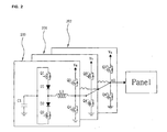
- the plasma display apparatus comprises an energy supply/recovery circuit unit 506 comprising a plurality of energy supply/recovery circuits 500, 501 and 502, and a sustain voltage circuit unit 507 comprising a plurality of sustain voltage circuits 503, 504 and 505.
- the energy supply/recovery circuit unit 506 and the sustain voltage circuit unit 507 form a sustain circuit (not shown).
- the energy supply/recovery circuits 500, 501 and 502 supply energy to the plasma display panel and recover reactive energy from the plasma display panel.
- the energy supply/recovery circuits 500, 501 and 502 of the energy supply/recovery circuit unit 506 are commonly connected to a first node n1 as an output terminal. Therefore, the energy supply/recovery circuit unit 506 has the first node n1 as the output terminal.
- the energy supply/recovery circuits 500, 501 and 502 are connected in parallel.
- the plurality of sustain voltage circuits 503, 504 and 505 maintain a voltage of the plasma display panel at a predetermined voltage.
- the plurality of sustain voltage circuits 503, 504 and 505 maintain the voltage of the plasma display panel at a sustain voltage Vs or a ground level voltage GND for a predetermined duration of time.
- Input terminals of the plurality of sustain voltage circuits 503, 504 and 505 are commonly connected to the output terminal n1 of the energy supply/recovery circuit unit 506.
- the plurality of sustain voltage circuits 503, 504 and 505 of the sustain voltage circuit unit 507 are commonly connected to a second node n2 as an output terminal. Therefore, the sustain voltage circuit unit 507 has the second node n2 as the output terminal.
- the plurality of sustain voltage circuits 503, 504 and 505 are connected in parallel.
- the plurality of energy supply/recovery circuits 500, 501 and 502 of the energy supply/recovery circuit unit 506 are integrated with one another and are formed on a single board.
- the plurality of sustain voltage circuits 503, 504 and 505 of the sustain voltage circuit unit 507 may be integrated one another or may be formed on a plurality of boards.
- the plurality of sustain voltage circuits 503, 504 and 505 are formed on two boards.
- the energy supply/recovery circuit unit 506 and the sustain voltage circuit unit 507 of the sustain circuit unit are formed on different boards. Accordingly, although electrical components of the plasma display apparatus according to the first embodiment have different driving characteristics, electrical damage or thermal damage of the electrical components caused by a difference between their driving characteristics is prevented.
- the plurality of energy supply/recovery circuits 500, 501 and 502 of the energy supply/recovery circuit unit 506 each comprise an energy storing unit, energy supply control units Q1a, Q1b and Q1c, energy recovery control units Q2a, Q2b and Q2c, first diodes D1a, D1b and D1c, second diodes D2a, D2b and D2c.
- the energy storing unit comprises energy storing capacitors Ca, Cb and Cc.
- the energy storing capacitors Ca, Cb and Cc recover and store reactive energy of the plasma display panel.
- the energy supply control units Q1a, Q1b and Q1c are turned on in an energy supply period such that the energy stored in the energy storing unit is supplied to the plasma display panel.
- the energy recovery control units Q2a, Q2b and Q2c are turned on in an energy recovery period such that reactive energy of the plasma display panel is stored in the energy storing unit.
- the plurality of sustain voltage circuits 503, 504 and 505 of the sustain voltage circuit unit 507 each comprise inductor units La, Lb and Lc, sustain voltage supply units Q3a, Q3b and Q3c, and ground voltage supply units Q4a, Q4b and Q4c.
- the inductor units La, Lb and Lc are connected between the output terminal n1 of the energy supply/recovery circuit unit 506 and the plasma display panel.
- the sustain voltage supply units Q3a, Q3b and Q3c supply the sustain voltage Vs supplied from a sustain voltage source to the plasma display panel in a sustain voltage maintenance period.
- the ground voltage supply units Q4a, Q4b and Q4c supply the ground level voltage GND supplied from a ground voltage source to the plasma display panel in a ground voltage maintenance period.
- the voltage stored in the energy storing capacitor Ca of the energy supply/recovery circuit 500, the voltage stored in the energy storing capacitor Cb of the energy supply/recovery circuit 501, and the voltage stored in the energy storing capacitor Cc of the energy supply/recovery circuit 502 is supplied to the first node n1.
- the voltage supplied to the first node n1 is distributed into the inductor units La, Lb and Lc of the sustain voltage circuits 503, 504 and 505
- the energy associated with the voltage distributed into the inductor units La, Lb and Lc is supplied to the plasma display panel through the second node n2 by LC resonance between capacitance of the discharge cells of the plasma display panel and inductance of the inductor units La, Lb and Lc.
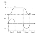
- the voltage Vp of the plasma display panel rises up to the sustain voltage Vs as illustrated in State 1 of FIG. 6. Further, the peak current flowing in the inductor units La, Lb and Lc equals +I L , since the energy is supplied from the energy storing capacitors Ca, Cb and Cc to the plasma display panel.
- the sustain voltage supply units Q3a, Q3b and Q3c of the sustain voltage circuits 503, 504 and 505 are turned on in the sustain voltage maintenance period (state 2).
- the sustain voltage Vs supplied from the sustain voltage source is supplied to the plasma display panel through the sustain voltage supply units Q3a, Q3b and Q3c and the second node n2.
- the voltage Vp of the plasma display panel is maintained at the sustain voltage Vs as illustrated in state 2 of FIG. 6 such that the sustain discharge is generated in the plasma display panel.
- the energy recovery control units Q2a, Q2b and Q2c of the energy supply/recovery circuits 500, 501 and 502 are turned on in the energy recovery period (state 3) subsequent to the sustain voltage maintenance period (state 2).
- the reactive energy of the plasma display panel with a voltage component is stored in the energy storing capacitors Ca, Cb and Cc through the second node n2, the inductor units La, Lb and Lc, the first node n1, the second diodes D2a, D2b and D2c, and the energy recovery control units Q2a, Q2b and Q2c.
- the voltage Vp of the plasma display panel falls from the sustain voltage Vs to the ground level voltage GND as illustrated in state 3 of FIG. 6. Further, the peak current flowing in the inductor units La, Lb and Lc equals -I L , since the energy is supplied from the plasma display panel to the energy storing capacitors Ca, Cb and Cc.
- the ground voltage supply units Q4a, Q4b and Q4c of the sustain voltage circuits 503, 504 and 505 are turned on in the ground voltage maintenance period (state 4). Therefore, the ground level voltage GND supplied form the ground voltage source is supplied to the plasma display panel through the ground voltage supply units Q4a, Q4b and Q4c and the second node n2.
- the voltage Vp of the plasma display panel is maintained at the ground level voltage GND as illustrated in state 4 of FIG. 6. Since a current does not flow in the inductor units La, Lb and Lc of the sustain voltage circuits 503, 504 and 505, the current flowing in the inductor units La, Lb and Lc equals to 0 in theory.
- the plurality of energy supply/recovery circuits 500, 501 and 502 are formed on a single board.
- the energy supply/recovery circuits 500, 501 and 502 have the first node n1 as the common output terminal. Accordingly, although the driving characteristics of the energy supply control units Q1a, Q1b and Q1c of the energy supply/recovery circuits 500, 501 and 502 differ from one another, a maximum magnitude of the load in one electrical component, that is, one of the energy supply control units Q1a, Q1b and Q1c is limited to the maximum voltage supplied by the energy storing capacitors Ca, Cb and Cc.
- the energy supply control unit Q1a of the energy supply/recovery circuit 500 is turned on at a time point t0
- the energy supply control unit Q1b of the energy supply/recovery circuit 501 is turned on at a time point t1 later than the time point t0 by ⁇ t
- the energy supply control unit Q1c of the energy supply/recovery circuit 502 is turned on at a time point t2 later than the time point t1 by ⁇ t.
- the energy supply control unit Q1a is turned on more rapidly than the energy supply control units Q1b and Q1c.
- the energy supply control unit Q1a only has to handle the energy supplied by Ca.
- the maximum magnitude of the load received to one electrical component is less than the prior art driving apparatus.
- the energy supply/recovery circuit unit 506 comprising the energy supply/recovery circuits 500, 501 and 502 is formed on a single board and outputs the resultant energy to one output terminal, that is, the first node n1. Accordingly, even if a driving deviation between the electrical components of the energy supply/recovery circuits 500, 501 and 502 is generated, the energy supply/recovery circuit unit 506 outputs the approximately regular result to the first node n1.
- the sustain voltage circuit unit 507 receives a stable input signal through the first node n1 of the energy supply/recovery circuit unit 506, irrespective of the driving deviation between the electrical components of the energy supply/recovery circuit unit 506.
- the sustain voltage circuits 503, 504 and 505 are driven more stably than the prior art driving apparatus.
- the sustain voltage circuits 503, 504 and 505 are formed on the plurality of boards, and have the common input terminal n1 and the common output terminal n2. Therefore, even if the driving characteristics of the electrical components of the energy supply/recovery circuits 500, 501 and 502 differ from one another, the maximum magnitude of the load of any one of the electrical components is less than the prior art driving apparatus.
- the sustain voltage supply unit Q3a when there is a driving difference between the electrical components, for example, when a turn-on time point of the sustain voltage supply unit Q3a is earlier than turn-on time points of the sustain voltage supply units Q3b and Q3c, the sustain voltage supply unit Q3a is loaded by the sum of driving deviation of each of the sustain voltage circuits 503, 504 and 505.
- the maximum magnitude of load for the electrical components of the sustain voltage circuit unit 507 is limited to the cumulative driving difference between the electrical components of the sustain voltage circuit unit 507.
- the maximum magnitude of load for the plurality of electrical components is less than in the prior art driving apparatus. Further, the load for the plurality of electrical components is distributed. Therefore, problems such as the concentration in generation of heat, an increase in power consumption, an electrical damage or a thermal damage of electrical components can be improved.
- a plasma display apparatus comprises a plurality of sustain circuits 703 and 704 which correspond to different regions of a plasma display panel 700, respectively.
- the first sustain circuit 703 corresponds to a first region 701 of the plasma display panel 700
- the second sustain circuit 704 corresponds to a second region 702 of the plasma display panel 700.
- the first sustain circuit 703 supplies a sustain voltage Vs to discharge cells included in the first region 701 of the plasma display panel 700. Further, the first sustain circuit 703 recovers reactive energy from the discharge cells in an energy recovery period.
- the second sustain circuit 704 supplies a sustain voltage Vs to discharge cells included in the second region 702 of the plasma display panel 700. Further, the second sustain circuit 704 recovers reactive energy from the discharge cells in an energy recovery period.
- the plasma display panel 700 is divided into two regions in FIG. 7. However, the plasma display panel 700 may be divided into three or more regions.
- the sustain circuits 703 and 704 drive the different regions of the plasma display panel 700, the maximum magnitude of load of one electrical component decreases.
- the sustain circuits 703 and 704 each comprise first and second energy supply/recovery circuits 703a and 704a and first and second sustain voltage circuits 703b and 704b.
- the first and second energy supply/recovery circuits 703a and 704a supply energy to the plasma display panel 700 and recover reactive energy from the plasma display panel 700.
- the first and second sustain voltage circuits 703b and 704b maintain a voltage of the plasma display panel 700 at a predetermined voltage.
- output terminals of the first and second energy supply/recovery circuits 703a and 704a are commonly connected to each other.
- the plasma display apparatus according to the second embodiment prevents the driving deviation generated in electrical components of the first and second energy supply/recovery circuits 703a and 704a from affecting the first and second sustain voltage circuits 703b and 704b. Accordingly, the maximum magnitude of load for one electrical component decreases.
- switching timing of the sustain circuits 703 and 704 is controlled by different timing controllers 705 and 706.
- the switching timing of the first sustain circuit 703 for driving the first region 701 of the plasma display panel 700 is controlled by the first timing controllers 705.
- the switching timing of the second sustain circuit 704 for driving the second region 702 of the plasma display panel 700 is controlled by the second timing controllers 706.
- the energy supply/recovery circuits 703a and 704a comprise energy storing units comprising energy storing capacitors Ca and Cb, and energy supply control units Q1a and Q1b.
- the energy supply control units Q1a and Q1b are turned on in an energy supply period to supply an energy stored in the energy storing units to the plasma display panel 700.
- the energy supply/recovery circuits 703a and 704a comprise energy recovery control units Q2a and Q2b, first diodes D1a and D1b, second diodes D2a and D2b.
- the energy recovery control units Q2a and Q2b are turned on in an energy recovery period such that a reactive energy of the plasma display panel 700 is stored in the energy storing unit.
- the first and second sustain voltage circuits 703b and 704b comprise first and second inductor units La and Lb connected between a common output terminal, that is, a first node n1 of the first and second energy supply/recovery circuits 703a and 704a and the first and second regions 701 and 702 of the plasma display panel 700.
- the first and second sustain voltage circuits 703b and 704b comprise first and second sustain voltage supply units Q3a and Q3b and first and second ground voltage supply units Q4a and Q4b.
- the sustain voltage supply units Q3a and Q3b supply the sustain voltage Vs supplied from a sustain voltage source in a sustain voltage maintenance period to the first and second regions 701 and 702 of the plasma display panel 700.
- the first and second ground voltage supply units Q4a and Q4b supply the ground level voltage GND supplied from a ground voltage source in a ground voltage maintenance period to the first and second regions 701 and 702 of the plasma display panel 700.
- the problems such as the concentration in generation of heat, increase in power consumption, electrical damage or thermal damage of electrical components are improved.
Landscapes
- Engineering & Computer Science (AREA)
- Physics & Mathematics (AREA)
- Power Engineering (AREA)
- Plasma & Fusion (AREA)
- Computer Hardware Design (AREA)
- General Physics & Mathematics (AREA)
- Theoretical Computer Science (AREA)
- Control Of Indicators Other Than Cathode Ray Tubes (AREA)
- Control Of Gas Discharge Display Tubes (AREA)
Abstract
Description
- This document relates to a display apparatus. It more particularly relates to a plasma display apparatus.
- A plasma display apparatus is a type of display apparatus which comprises a plasma display panel and a driver for driving the plasma display panel.
- The plasma display panel comprises a front panel, a rear panel, and barrier ribs formed between the front panel and the rear panel. The barrier ribs form discharge cells. Each of the discharge cells is filled with an inert gas containing a main discharge gas such as neon (Ne), helium (He) or a Ne-He gas mixture and a small amount of xenon (Xe).
- When a high frequency voltage generates a discharge, the inert gas within the discharge cells generates vacuum ultraviolet radiation. The vacuum ultraviolet radiation excites phosphors formed between the barrier ribs to emit visible light such that an image is displayed. Since the above-described type of plasma display panel can be manufactured to be thin and light, the plasma display panel has been considered as a next generation display apparatus.
- FIG. 1 illustrates a prior art driving apparatus of a prior art plasma display panel.
- Referring to FIG. 1, a prior art driving apparatus of a plasma display panel comprises a
sustain circuit unit 100, asetup supply unit 110, a negative polarity scanvoltage supply unit 120, a set-down supply unit 130, a scan referencevoltage supply unit 140, a drive integrated circuit (IC) 150, a seventh switch Q7 connected between thesetup supply unit 110 and thedrive IC 150, and a sixth switch Q6 connected between thesustain circuit unit 100 and thesetup supply unit 110. - The drive IC 150 is connected in a push-pull configuration. The
drive IC 150 comprises a twelfth switch Q12 and a thirteenth switch Q13 for receiving a voltage signal from thesustain circuit unit 100, thesetup supply unit 110, the negative polarity scanvoltage supply unit 120, the set-down supply unit 130, and the scan referencevoltage supply unit 140. - An output line between the twelfth switch Q12 and the thirteenth switch Q13 is connected to one of plurality of scan electrodes of the plasma display panel Cp.
- The
sustain circuit unit 100 recovers energy from the panel Cp and supplies a sustain voltage Vs to the panel Cp. - The negative polarity scan
voltage supply unit 120 supplies a scan pulse having a voltage magnitude of-Vy to the scan electrodes in an address period. - The scan reference
voltage supply unit 140 supplies a scan reference voltage Vsc to the scan electrodes in the address period. - The set-down
supply unit 130 supplies a falling ramp pulse to the scan electrodes in a set-down period of a reset period. - The
setup supply unit 110 supplies a rising ramp pulse to the scan electrodes in a setup period of the reset period. - Generally, the plurality of
sustain circuit units 100 are formed on a single board. This will be described with reference to FIG. 2. - FIG. 2 illustrates an example of integrating a plurality of sustain circuit units into one module in a prior art driving apparatus of a plasma display panel.
- Referring to FIG. 2, a plurality of
sustain circuit units sustain circuit units - A reason for forming the plurality of
sustain circuit units sustain circuit units - For example, when only the
sustain circuit unit 200 supplies all of the sustain voltage Vs, electrical components, for example, an energy storing capacitor C1, a first switch Q1, a second switch Q2, a third switch Q3, a fourth switch Q4, a first diode D1, a second diode D2 and a first inductor L1 of thesustain circuit unit 200 must have a high withstanding voltage characteristic. Consequently, the fabricating cost of the driving apparatus increases. - Further, the generation of heat and conduction resistance (Rds) in the electrical components of the
sustain circuit unit 200 increase. - Accordingly, as illustrated in FIG. 2, the forming of the plurality of
sustain circuit units sustain circuit units - There is a strong likelihood that a deviation between the driving characteristics of the electrical components of the
sustain circuit units - In theory, the electrical components having an equal function need to have equal driving characteristics. However, variations in the fabricating processes of the electrical components cause differences between the driving characteristics of the electrical components.
- As the size of a plasma display panel becomes larger and the number of electrical components used in the driving apparatus of the plasma display panel increases, the differences between the driving characteristics of the electrical components becomes greater. Accordingly, when driving the plasma display panel, there can be problems such as the concentration of generation of heat, an increase in power consumption, and damages to electrical components.
- For example, suppose that the
sustain circuit unit 200 supplies the sustain voltage Vs at a time point t0, thesustain circuit unit 201 supplies the sustain voltage Vs at a time point t1 later than the time point t0 by Δt, and thesustain circuit unit 202 supplies the sustain voltage Vs at a time point t2 later than the time point t1 by Δt. - In other words, the
sustain circuit unit 200 supplies the sustain voltage Vs more rapidly than thesustain circuit units - Therefore, load of the sustain voltage Vs is concentrated on the
sustain circuit unit 200. - Since load of the sustain voltage Vs is concentrated on the
sustain circuit unit 200, excessive heat is generated in the driving apparatus and the electrical components of thesustain circuit unit 200 will become electrically or thermally damaged. - The present invention seeks to provide an improved plasma display apparatus.
- Embodiments of the present invention can provide a plasma display apparatus capable of preventing the excessive generation of heat and damage caused by a differences between driving characteristics in a sustain circuit unit.
- A plasma display apparatus according to an aspect of the invention comprises a plasma display panel comprising an electrode, a sustain voltage circuit unit comprising a plurality of sustain voltage circuits, arranged to maintain a voltage of the plasma display panel at a predetermined voltage and comprising a common input terminal, and an energy supply/recovery circuit unit comprising a plurality of energy supply/recovery circuits arranged to supply and recover energy to and from the plasma display panel, the plurality of energy supply/recovery circuits comprising a common output terminal and being connected to the sustain voltage circuit unit.
- The common output terminal of the energy supply/recovery circuit unit and the common input terminal of the sustain voltage circuit unit may be commonly connected to each other.
- The plurality of sustain voltage circuits may comprise a common output terminal.
- The energy supply/recovery circuit unit may be formed on a single board by combining the plurality of energy supply/recovery circuits.
- The sustain voltage circuit unit may be formed on a plurality of boards by combining the plurality of sustain voltage circuits.
- The plurality of boards may equal two.
- The plurality of energy supply/recovery circuits may comprise an energy storing unit comprising a capacitor, an energy supply control unit arranged to supply energy stored in the energy storing unit to the plasma display panel, and an energy recovery control unit arranged to store reactive energy of the plasma display panel in the energy storing unit.
- The plurality of sustain voltage circuits may comprise an inductor unit connected between the output terminal of the energy supply/recovery circuit unit and the plasma display panel, a sustain voltage supply unit arranged to supply a sustain voltage to the plasma display panel, and a ground voltage supply unit arranged to supply a ground level voltage to the plasma display panel.
- A plasma display apparatus according to an aspect of the invention comprises a plasma display panel comprising an electrode, a sustain voltage circuit unit, in which a plurality of sustain voltage circuits arranged to maintain a voltage of the plasma display panel at a predetermined voltage are connected in parallel, and an energy supply/recovery circuit unit, in which a plurality of energy supply/recovery circuits arranged to supply and recover energy to and from the plasma display panel are connected to the sustain voltage circuit unit and are connected in parallel.
- A common output terminal of the energy supply/recovery circuit unit and a common input terminal of the sustain voltage circuit unit may be commonly connected to each other.
- The plurality of sustain voltage circuits may comprise a common output terminal.
- The energy supply/recovery circuit unit may be formed on a single board by combining the plurality of energy supply/recovery circuits.
- The sustain voltage circuit unit may be formed on a plurality of boards by combining the plurality of sustain voltage circuits.
- The plurality of boards may equal two.
- The plurality of energy supply /recovery circuits may comprise an energy storing unit comprising a capacitor, an energy supply control unit arranged to supply energy stored in the energy storing unit to the plasma display panel, and an energy recovery control unit arranged to store reactive energy of the plasma display panel in the energy storing unit.
- The plurality of sustain voltage circuits may comprise an inductor unit connected between the output terminal of the energy supply/recovery circuit and the plasma display panel, a sustain voltage supply unit arranged to supply a sustain voltage to the plasma display panel, and a ground voltage supply unit arranged to supply a ground level voltage to the plasma display panel.
- A plasma display apparatus according to another aspect of the present invention comprises a plasma display panel arranged to be driven by dividing the plasma display panel into a plurality of regions, a first sustain circuit comprising a first energy supply/recovery circuit arranged to supply and recover energy to and from a first region of the plasma display panel, and a first sustain voltage circuit arranged to maintain a voltage of the first region at a predetermined voltage, and a second sustain circuit comprising a second energy supply/recovery circuit arranged to supply and recover energy to and from a second region of the plasma display panel, and a second sustain voltage circuit arranged to maintain a voltage of the second region at a predetermined voltage, wherein an output terminal of the first energy supply/ recovery circuit and an output terminal of the second energy supply/recovery circuit are commonly connected to each other.
- The switching timing of the first sustain circuit may be controlled by a first timing controller, and switching timing of the second sustain circuit may be controlled by a second timing controller.
- The first energy supply/recovery circuit may comprise a first energy storing unit comprising a capacitor, a first energy supply control unit arranged to supply energy stored in the first energy storing unit to the first region, and a first energy recovery control unit arranged to store reactive energy of the first region in the first energy storing unit.
- The first sustain voltage circuit may comprise a first inductor unit connected between the output terminal of the first energy supply/recovery circuit and the first region, a first sustain voltage supply unit arranged to supply a sustain voltage to the first region, and a first ground voltage supply unit arranged to supply a ground level voltage to the first region.
- The second energy supply/recovery circuit may comprise a second energy storing unit comprising a capacitor, a second energy supply control unit arranged to supply energy stored in the second energy storing unit to the second region, and a second energy recovery control unit arranged to store reactive energy of the second region in the second energy storing unit.
- The second sustain voltage circuit may comprise a second inductor unit which is connected between the output terminal of the second energy supply/recovery circuit and the second region, a second sustain voltage supply unit arranged to supply a sustain voltage to the second region, and a second ground voltage supply unit arranged to supply a ground level voltage to the second region.
- Embodiments of the invention will now be described in detail by way of non-limiting example only, with reference to the drawings, in which like numerals refer to like elements.
- FIG. 1 illustrates a prior art driving apparatus of a plasma display panel;
- FIG. 2 illustrates an example of integrating a plurality of sustain circuit units into one module in a prior art driving apparatus of a plasma display panel;
- FIG. 3 illustrates a structure of a plasma display panel of a plasma display apparatus according to a first embodiment of the invention;
- FIG. 4 illustrates a method of driving the plasma display apparatus according to the first embodiment;
- FIG. 5 illustrates a structure of the plasma display apparatus according to the first embodiment;
- FIG. 6 illustrates an operation of the plasma display apparatus according to the first embodiment; and
- FIG. 7 illustrates a structure of a plasma display apparatus according to a second embodiment of the invention.
- As illustrated in FIG. 3, a plasma display panel comprises a
front panel 300 and arear panel 310 which are coupled in parallel facing each other with a predetermined distance therebetween. A plurality of scan electrodes 302 and a plurality of sustainelectrodes 303 are formed in pairs on afront glass substrate 301 of thefront panel 310, being a display surface on which an image can be displayed, to form a plurality of maintenance electrode pairs. A plurality ofaddress electrodes 313 are arranged on arear glass substrate 311 of therear panel 310 constituting a rear surface to intersect the plurality of maintenance electrode pairs. - The scan electrode 302 and the sustain
electrode 303 each comprise respectivetransparent electrodes bus electrodes electrode 303 in one discharge cell to maintain emissions of cells selected for discharge. - The scan electrode 302 and the sustain
electrode 303 are covered with one or more upperdielectric layers 304 for limiting the discharge current and providing insulation between the maintenance electrode pairs. A protective layer 305 with a deposit of MgO is formed on an upper surface of theupper dielectric layer 304 to facilitate discharge conditions. - A plurality of stripe-type (or well-type)
barrier ribs 312 are formed in parallel on therear glass substrate 311 of therear panel 310 to form a plurality of discharge spaces, that is, a plurality of discharge cells. The plurality ofaddress electrodes 313 are arranged in parallel with thebarrier ribs 312 to perform an address discharge and generate vacuum ultraviolet radiation. - Red (R), green (G) and blue (B)
phosphors 314 are coated on an upper surface of therear glass substrate 311 and emit visible light for displaying an image during the generation of the address discharge. A lowerdielectric layer 315 is formed between theaddress electrodes 313 and thephosphors 314 to protect theaddress electrodes 313. - To drive the plasma display panel having the above-described structure, a method of driving the plasma display apparatus will be described with reference to FIG. 4.
- As illustrated in FIG. 4, the plasma display panel is driven by dividing each of subfields into a reset period for initializing all cells, an address period for selecting cells to be discharged, a sustain period for maintaining discharges of the selected cells, and an erasure period for erasing wall charges within the discharged cells.
- In the reset period, a rising ramp waveform Ramp-up is simultaneously supplied to all scan electrodes Y1 to Ym during a setup period. The rising ramp waveform Ramp-up generates a weak dark discharge within the discharge cells of the entire screen. The weak dark discharge is called a setup discharge.
- By performing the setup discharge, positive wall charges are accumulated on address electrodes X1 to Xn and sustain electrodes Z, and negative wall charges are accumulated on the scan electrodes Y1 to Ym.
- In a set-down period of the reset period, a falling ramp waveform Ramp-down, which falls from a positive voltage lower than a peak voltage of the rising ramp waveform to a specific voltage of a ground level voltage GND or less, is supplied to the scan electrodes Y1 to Ym to generate a weak erasure discharge within the cells. The weak erase discharge sufficiently erases the wall charges excessively accumulated on the scan electrodes Y1 to Ym. The weak erase discharge is called a set-down discharge.
- By performing the set-down discharge, the wall charges uniformly remain within the cells to the degree that there is the generation of a stable address discharge.
- In the address period, a negative polarity scan pulse Sp is sequentially supplied to the scan electrodes Y1 to Ym and, at the same time, a positive polarity data pulse Dp synchronized with the scan pulse Sp is supplied to the address electrodes X1 to Xn.
- While the voltage difference between the negative polarity scan pulse Sp and the positive polarity data pulse Dp is added to the wall charges produced during the reset period, the address discharge is generated within the discharge cells to which the data pulse Dp is supplied.
- The wall charges necessary for a sustain discharge when supplying a sustain voltage Vs are formed within the cells selected by performing the address discharge.
- A positive voltage Vz is supplied to the sustain electrodes Z during the set-down period and the address period to decrease the voltage difference between the sustain electrodes Z and the scan electrodes Y1 to Ym. Accordingly, an erroneous discharge between the sustain electrodes Z and the scan electrodes Y1 to Ym is prevented.
- In the sustain period, a sustain pulse SUSp is alternately supplied to the scan electrodes Y1 to Ym and the sustain electrodes Z.
- While the wall voltage within the cells selected by performing the address discharge is added to the sustain pulse SUSp, a sustain discharge, that is, a display discharge, is generated between the scan electrodes Y1 to Ym and the sustain electrodes Z whenever the sustain pulse SUSp is supplied.
- After completing the sustain discharge, in the erasure period, an erasure ramp waveform Ramp-ers with a narrower pulse width and a low level voltage is supplied to the sustain electrodes Z to erase the wall charges remaining within the cells of the whole screen.
- As illustrated in FIG. 5, the plasma display apparatus according to the first embodiment comprises an energy supply/
recovery circuit unit 506 comprising a plurality of energy supply/recovery circuits voltage circuit unit 507 comprising a plurality of sustainvoltage circuits - The energy supply/
recovery circuit unit 506 and the sustainvoltage circuit unit 507 form a sustain circuit (not shown). - The energy supply/
recovery circuits - The energy supply/
recovery circuits recovery circuit unit 506 are commonly connected to a first node n1 as an output terminal. Therefore, the energy supply/recovery circuit unit 506 has the first node n1 as the output terminal. - In other words, the energy supply/
recovery circuits - The plurality of sustain
voltage circuits - For example, the plurality of sustain
voltage circuits - Input terminals of the plurality of sustain
voltage circuits recovery circuit unit 506. - The plurality of sustain
voltage circuits voltage circuit unit 507 are commonly connected to a second node n2 as an output terminal. Therefore, the sustainvoltage circuit unit 507 has the second node n2 as the output terminal. - In other words, the plurality of sustain
voltage circuits - It is preferable that the plurality of energy supply/
recovery circuits recovery circuit unit 506 are integrated with one another and are formed on a single board. - The plurality of sustain
voltage circuits voltage circuit unit 507 may be integrated one another or may be formed on a plurality of boards. - Preferably, the plurality of sustain
voltage circuits - In the plasma display apparatus according to the first embodiment, the energy supply/
recovery circuit unit 506 and the sustainvoltage circuit unit 507 of the sustain circuit unit are formed on different boards. Accordingly, although electrical components of the plasma display apparatus according to the first embodiment have different driving characteristics, electrical damage or thermal damage of the electrical components caused by a difference between their driving characteristics is prevented. - Characteristics of the plasma display apparatus according to the first embodiment will be described with reference to a description of the operation of the plasma display apparatus according to the first embodiment.
- The plurality of energy supply/
recovery circuits recovery circuit unit 506 each comprise an energy storing unit, energy supply control units Q1a, Q1b and Q1c, energy recovery control units Q2a, Q2b and Q2c, first diodes D1a, D1b and D1c, second diodes D2a, D2b and D2c. - The energy storing unit comprises energy storing capacitors Ca, Cb and Cc.
- The energy storing capacitors Ca, Cb and Cc recover and store reactive energy of the plasma display panel.
- The energy supply control units Q1a, Q1b and Q1c are turned on in an energy supply period such that the energy stored in the energy storing unit is supplied to the plasma display panel.
- The energy recovery control units Q2a, Q2b and Q2c are turned on in an energy recovery period such that reactive energy of the plasma display panel is stored in the energy storing unit.
- The plurality of sustain
voltage circuits voltage circuit unit 507 each comprise inductor units La, Lb and Lc, sustain voltage supply units Q3a, Q3b and Q3c, and ground voltage supply units Q4a, Q4b and Q4c. - The inductor units La, Lb and Lc are connected between the output terminal n1 of the energy supply/
recovery circuit unit 506 and the plasma display panel. - The sustain voltage supply units Q3a, Q3b and Q3c supply the sustain voltage Vs supplied from a sustain voltage source to the plasma display panel in a sustain voltage maintenance period.
- The ground voltage supply units Q4a, Q4b and Q4c supply the ground level voltage GND supplied from a ground voltage source to the plasma display panel in a ground voltage maintenance period.
- Operation of the sustain circuit comprising the energy supply/
recovery circuit unit 506 and the sustainvoltage circuit unit 507 will be described with reference to FIG. 6. - Suppose that the energy storing capacitors Ca, Cb and Cc are charged to a voltage of Vs/2.
- When the energy supply control units Q1a, Q1b and Q1c are turned on in the energy supply period (state 1), the voltage on the energy storing capacitors Ca, Cb and Cc is supplied to the first node n1 through the energy supply control units Q1a, Q1b and Q1c and the first diodes D1a, D1b and D1c.
- In other words, the voltage stored in the energy storing capacitor Ca of the energy supply/
recovery circuit 500, the voltage stored in the energy storing capacitor Cb of the energy supply/recovery circuit 501, and the voltage stored in the energy storing capacitor Cc of the energy supply/recovery circuit 502 is supplied to the first node n1. - The voltage supplied to the first node n1 is distributed into the inductor units La, Lb and Lc of the sustain
voltage circuits - The energy associated with the voltage distributed into the inductor units La, Lb and Lc is supplied to the plasma display panel through the second node n2 by LC resonance between capacitance of the discharge cells of the plasma display panel and inductance of the inductor units La, Lb and Lc.
- The voltage Vp of the plasma display panel rises up to the sustain voltage Vs as illustrated in
State 1 of FIG. 6. Further, the peak current flowing in the inductor units La, Lb and Lc equals +IL, since the energy is supplied from the energy storing capacitors Ca, Cb and Cc to the plasma display panel. - Next, the sustain voltage supply units Q3a, Q3b and Q3c of the sustain
voltage circuits - As a result, the sustain voltage Vs supplied from the sustain voltage source is supplied to the plasma display panel through the sustain voltage supply units Q3a, Q3b and Q3c and the second node n2.
- Therefore, the voltage Vp of the plasma display panel is maintained at the sustain voltage Vs as illustrated in state 2 of FIG. 6 such that the sustain discharge is generated in the plasma display panel.
- Since current does not flow in the inductor units La, Lb and Lc of the sustain
voltage circuits - The energy recovery control units Q2a, Q2b and Q2c of the energy supply/
recovery circuits - Therefore, the reactive energy of the plasma display panel with a voltage component is stored in the energy storing capacitors Ca, Cb and Cc through the second node n2, the inductor units La, Lb and Lc, the first node n1, the second diodes D2a, D2b and D2c, and the energy recovery control units Q2a, Q2b and Q2c.
- As a result, the voltage Vp of the plasma display panel falls from the sustain voltage Vs to the ground level voltage GND as illustrated in state 3 of FIG. 6. Further, the peak current flowing in the inductor units La, Lb and Lc equals -IL, since the energy is supplied from the plasma display panel to the energy storing capacitors Ca, Cb and Cc.
- The ground voltage supply units Q4a, Q4b and Q4c of the sustain
voltage circuits - The voltage Vp of the plasma display panel is maintained at the ground level voltage GND as illustrated in state 4 of FIG. 6. Since a current does not flow in the inductor units La, Lb and Lc of the sustain
voltage circuits - The plurality of energy supply/
recovery circuits - The energy supply/
recovery circuits recovery circuits - For example, suppose that the energy supply control unit Q1a of the energy supply/
recovery circuit 500 is turned on at a time point t0, the energy supply control unit Q1b of the energy supply/recovery circuit 501 is turned on at a time point t1 later than the time point t0 by Δt, and the energy supply control unit Q1c of the energy supply/recovery circuit 502 is turned on at a time point t2 later than the time point t1 by Δt. - In other words, the energy supply control unit Q1a is turned on more rapidly than the energy supply control units Q1b and Q1c.
- Therefore, if the total load of the energy storing capacitors Ca, Cb and Cc, the energy supply control unit Q1a only has to handle the energy supplied by Ca.
- In other words, the maximum magnitude of the load received to one electrical component is less than the prior art driving apparatus.
- The energy supply/
recovery circuit unit 506 comprising the energy supply/recovery circuits recovery circuits recovery circuit unit 506 outputs the approximately regular result to the first node n1. - Therefore, the sustain
voltage circuit unit 507 receives a stable input signal through the first node n1 of the energy supply/recovery circuit unit 506, irrespective of the driving deviation between the electrical components of the energy supply/recovery circuit unit 506. - Further, even if a driving deviation between the electrical components of the sustain
voltage circuits recovery circuits voltage circuits - In other words, the sustain
voltage circuits recovery circuits - More specifically, when there is a driving difference between the electrical components of the prior art driving apparatus of the plasma display panel of FIG. 2, excessive heat is generated in an electrical component or the electrical component becomes damaged. For example, when in switches Q3, Q3' and Q3" of the sustain
circuit units 100, 101 and 102 connected to the sustain voltage source for supplying the sustain voltage Vs, a turn-on time point of the switch Q3 is earlier than turn-on time points of the switches Q3' and Q3", the sum of the total cumulative driving differences of each of the sustaincircuit units 100, 101 and 102 has to be handled by the switch Q3. Therefore, excessive heat is generated in the switch Q3 and the switch Q3 become damaged. - However, in the described exemplary embodiment of the invention, when there is a driving difference between the electrical components, for example, when a turn-on time point of the sustain voltage supply unit Q3a is earlier than turn-on time points of the sustain voltage supply units Q3b and Q3c, the sustain voltage supply unit Q3a is loaded by the sum of driving deviation of each of the sustain
voltage circuits - In other words, since the energy supply/
recovery circuits recovery circuit unit 506 among all of the electrical components of the driving apparatus is compensated for. - Since a signal for compensating the driving deviation between the electrical components of the energy supply/
recovery circuit unit 506 is supplied to the sustainvoltage circuit unit 507 as an input signal, the maximum magnitude of load for the electrical components of the sustainvoltage circuit unit 507 is limited to the cumulative driving difference between the electrical components of the sustainvoltage circuit unit 507. - Accordingly, in the driving apparatus of an embodiment of the present invention, the maximum magnitude of load for the plurality of electrical components is less than in the prior art driving apparatus. Further, the load for the plurality of electrical components is distributed. Therefore, problems such as the concentration in generation of heat, an increase in power consumption, an electrical damage or a thermal damage of electrical components can be improved.
- Referring to FIG. 7, a plasma display apparatus according to a second embodiment of the invention comprises a plurality of sustain
circuits plasma display panel 700, respectively. - For example, the first sustain
circuit 703 corresponds to afirst region 701 of theplasma display panel 700, and the second sustaincircuit 704 corresponds to asecond region 702 of theplasma display panel 700. - In other words, the first sustain
circuit 703 supplies a sustain voltage Vs to discharge cells included in thefirst region 701 of theplasma display panel 700. Further, the first sustaincircuit 703 recovers reactive energy from the discharge cells in an energy recovery period. - The second sustain
circuit 704 supplies a sustain voltage Vs to discharge cells included in thesecond region 702 of theplasma display panel 700. Further, the second sustaincircuit 704 recovers reactive energy from the discharge cells in an energy recovery period. - The
plasma display panel 700 is divided into two regions in FIG. 7. However, theplasma display panel 700 may be divided into three or more regions. - Since the sustain
circuits plasma display panel 700, the maximum magnitude of load of one electrical component decreases. - The sustain
circuits recovery circuits voltage circuits recovery circuits plasma display panel 700 and recover reactive energy from theplasma display panel 700. The first and second sustainvoltage circuits plasma display panel 700 at a predetermined voltage. - It is preferable that output terminals of the first and second energy supply/
recovery circuits - In the same way as the plasma display apparatus according to the first embodiment, the plasma display apparatus according to the second embodiment prevents the driving deviation generated in electrical components of the first and second energy supply/
recovery circuits voltage circuits - Further, the problems such as the concentration in generation of heat, increase in power consumption, electrical damage or thermal damage of electrical components are improved.
- It is preferable that switching timing of the sustain
circuits different timing controllers - For example, the switching timing of the first sustain
circuit 703 for driving thefirst region 701 of theplasma display panel 700 is controlled by thefirst timing controllers 705. The switching timing of the second sustaincircuit 704 for driving thesecond region 702 of theplasma display panel 700 is controlled by thesecond timing controllers 706. - The energy supply/
recovery circuits plasma display panel 700. - Further, the energy supply/
recovery circuits plasma display panel 700 is stored in the energy storing unit. - The first and second sustain
voltage circuits recovery circuits second regions plasma display panel 700. - The first and second sustain
voltage circuits second regions plasma display panel 700. The first and second ground voltage supply units Q4a and Q4b supply the ground level voltage GND supplied from a ground voltage source in a ground voltage maintenance period to the first andsecond regions plasma display panel 700. - Since operations of the plasma display apparatus according to the second embodiment is substantially the same as the operations of the plasma display apparatus according to the first embodiment, a description thereof is omitted.
- In the plasma display apparatus according to the second embodiment the problems such as the concentration in generation of heat, increase in power consumption, electrical damage or thermal damage of electrical components are improved.
- The invention being thus described, it will be obvious that the same may be varied in many ways. Such variations are not to be regarded as a departure from the scope of the invention, and all such modifications as would be obvious to one skilled in the art are intended to be included within the scope of the following claims.
Claims (20)
- A plasma display apparatus comprising:a plasma display panel comprising an electrode;a sustain voltage circuit unit comprising a plurality of sustain voltage circuits, arranged to maintain a voltage of the plasma display panel at a predetermined voltage and comprising a common input terminal; andan energy supply/recovery circuit unit comprising a plurality of energy supply/recovery circuits arranged to supply and recover energy to and from the plasma display panel, the plurality of energy supply/recovery circuits comprising a common output terminal and being connected to the sustain voltage circuit unit.
- The plasma display apparatus of claim 1, wherein the common output terminal of the energy supply/recovery circuit unit and the common input terminal of the sustain voltage circuit unit are commonly connected to each other.
- The plasma display apparatus of claim 1, wherein the plurality of sustain voltage circuits comprise a common output terminal.
- The plasma display apparatus of claim 1, wherein the energy supply/recovery circuit unit is formed on a single board by combining the plurality of energy supply/recovery circuits.
- The plasma display apparatus of claim 1, wherein the sustain voltage circuit unit is formed on a plurality of boards by combining the plurality of sustain voltage circuits.
- The plasma display apparatus of claim 5, wherein the plurality of boards equals two.
- The plasma display apparatus of claim 1, wherein the plurality of energy supply/recovery circuits comprises
an energy storing unit comprising a capacitor,
an energy supply control unit arranged to supply energy stored in the energy storing unit to the plasma display panel, and
an energy recovery control unit arranged to store reactive energy of the plasma display panel in the energy storing unit. - The plasma display apparatus of claim 1, wherein the plurality of sustain voltage circuits comprises
an inductor unit connected between the output terminal of the energy supply/recovery circuit unit and the plasma display panel,
a sustain voltage supply unit arranged to supply a sustain voltage to the plasma display panel, and
a ground voltage supply unit arranged to supply a ground level voltage to the plasma display panel. - A plasma display apparatus comprising:a plasma display panel comprising an electrode;a sustain voltage circuit unit, in which a plurality of sustain voltage circuits are arranged to maintain a voltage of the plasma display panel at a predetermined voltage and are connected in parallel; andan energy supply/recovery circuit unit, in which a plurality of energy supply/recovery circuits are arranged to supply and recover energy to and from the plasma display panel, are connected to the sustain voltage circuit unit, and are connected in parallel.
- The plasma display apparatus of claim 9, wherein a common output terminal of the energy supply/recovery circuit unit and a common input terminal of the sustain voltage circuit unit are commonly connected to each other.
- The plasma display apparatus of claim 9, wherein the plurality of sustain voltage circuits comprise a common output terminal.
- The plasma display apparatus of claim 9, wherein the energy supply/recovery circuit unit is formed on a single board by combining the plurality of energy supply/recovery circuits.
- The plasma display apparatus of claim 9, wherein the plurality of energy supply /recovery circuits comprises
an energy storing unit comprising a capacitor,
an energy supply control unit arranged to supply energy stored in the energy storing unit to the plasma display panel, and
an energy recovery control unit arranged to store reactive energy of the plasma display panel in the energy storing unit. - The plasma display apparatus of claim 9, wherein the plurality of sustain voltage circuits comprises
an inductor unit connected between the output terminal of the energy supply/recovery circuit and the plasma display panel,
a sustain voltage supply unit arranged to supply a sustain voltage to the plasma display panel, and
a ground voltage supply unit arranged to supply a ground level voltage to the plasma display panel. - A plasma display apparatus comprising:a plasma display panel arranged to be driven by dividing the plasma display panel into a plurality of regions;a first sustain circuit comprising a first energy supply/recovery circuit arranged to supply and recover energy to and from a first region of the plasma display panel, and a first sustain voltage circuit arranged to maintain a voltage of the first region at a predetermined voltage; anda second sustain circuit comprising a second energy supply/recovery circuit arranged to supply and recover energy to and from a second region of the plasma display panel, and a second sustain voltage circuit arranged to maintain a voltage of the second region at a predetermined voltage,wherein an output terminal of the first energy supply/ recovery circuit and an output terminal of the second energy supply/recovery circuit are commonly connected to each other.
- The plasma display apparatus of claim 15, wherein switching timing of the first sustain circuit is arranged to be controlled by a first timing controller, and switching timing of the second sustain circuit is arranged to be controlled by a second timing controller.
- The plasma display apparatus of claim 15, wherein the first energy supply/recovery circuit comprises
a first energy storing unit comprising a capacitor,
a first energy supply control unit arranged to supply energy stored in the first energy storing unit to the first region, and
a first energy recovery control unit arranged to store reactive energy of the first region in the first energy storing unit. - The plasma display apparatus of claim 15, wherein the first sustain voltage circuit comprises
a first inductor unit connected between the output terminal of the first energy supply/recovery circuit and the first region,
a first sustain voltage supply unit arranged to supply a sustain voltage to the first region, and
a first ground voltage supply unit arranged to supply a ground level voltage to the first region. - The plasma display apparatus of claim 15, wherein the second energy supply/recovery circuit comprises
a second energy storing unit comprising a capacitor,
a second energy supply control unit arranged to supply energy stored in the second energy storing unit to the second region, and
a second energy recovery control unit arranged to store reactive energy of the second region in the second energy storing unit. - The plasma display apparatus of claim 15, wherein the second sustain voltage circuit comprises
a second inductor unit which is connected between the output terminal of the second energy supply/recovery circuit and the second region,
a second sustain voltage supply unit arranged to supply a sustain voltage to the second region, and
a second ground voltage supply unit arranged to supply a ground level voltage to the second region.
Applications Claiming Priority (1)
| Application Number | Priority Date | Filing Date | Title |
|---|---|---|---|
| KR1020050052098A KR100705814B1 (en) | 2005-06-16 | 2005-06-16 | Driving device of plasma display panel |
Publications (1)
| Publication Number | Publication Date |
|---|---|
| EP1734498A1 true EP1734498A1 (en) | 2006-12-20 |
Family
ID=36950429
Family Applications (1)
| Application Number | Title | Priority Date | Filing Date |
|---|---|---|---|
| EP06253103A Withdrawn EP1734498A1 (en) | 2005-06-16 | 2006-06-15 | Plasma display apparatus |
Country Status (5)
| Country | Link |
|---|---|
| US (1) | US20060284799A1 (en) |
| EP (1) | EP1734498A1 (en) |
| JP (1) | JP2006350357A (en) |
| KR (1) | KR100705814B1 (en) |
| CN (1) | CN1881396A (en) |
Cited By (1)
| Publication number | Priority date | Publication date | Assignee | Title |
|---|---|---|---|---|
| EP2154670A3 (en) * | 2008-08-11 | 2010-12-01 | Samsung SDI Co., Ltd. | Plasma display |
Families Citing this family (2)
| Publication number | Priority date | Publication date | Assignee | Title |
|---|---|---|---|---|
| KR20080004085A (en) * | 2006-07-04 | 2008-01-09 | 엘지전자 주식회사 | Address driving apparatus and method of plasma display panel |
| US8259037B2 (en) * | 2008-06-18 | 2012-09-04 | Samsung Sdi Co., Ltd. | Plasma display and driving apparatus thereof |
Citations (3)
| Publication number | Priority date | Publication date | Assignee | Title |
|---|---|---|---|---|
| EP0896316A1 (en) * | 1997-08-08 | 1999-02-10 | Pioneer Electronic Corporation | Driving apparatus for plasma display panel |
| US5943030A (en) * | 1995-11-24 | 1999-08-24 | Nec Corporation | Display panel driving circuit |
| EP1333419A2 (en) | 2001-12-11 | 2003-08-06 | Samsung Electronics Co., Ltd. | Driving circuit for sequentially discharging and driving sustain discharge electrodes of a plasma display |
Family Cites Families (14)
| Publication number | Priority date | Publication date | Assignee | Title |
|---|---|---|---|---|
| KR100222203B1 (en) * | 1997-03-17 | 1999-10-01 | 구자홍 | Energy Recovery Sustain Circuit for AC Plasma Display Panels |
| KR100277300B1 (en) * | 1997-12-31 | 2001-01-15 | 황기웅 | Power recovery drive circuit of AC plasma display |
| KR20000009133A (en) * | 1998-07-21 | 2000-02-15 | 구자홍 | Driving device for plasma display panel |
| JP2000047636A (en) * | 1998-07-30 | 2000-02-18 | Matsushita Electric Ind Co Ltd | AC type plasma display device |
| AU2001257111A1 (en) * | 2000-04-20 | 2001-11-07 | James C. Rutherford | Method for driving plasma display panel |
| US6917351B1 (en) * | 2001-02-06 | 2005-07-12 | Imaging Systems Technology | Energy recovery in plasma display panel |
| JP4651221B2 (en) * | 2001-05-08 | 2011-03-16 | パナソニック株式会社 | Display panel drive device |
| WO2003041041A2 (en) * | 2001-11-06 | 2003-05-15 | Pioneer Corporation | Displ ay panel driving apparatus with reduced power loss |
| KR100477990B1 (en) * | 2002-09-10 | 2005-03-23 | 삼성에스디아이 주식회사 | Plasma display panel and driving apparatus and method thereof |
| KR100484175B1 (en) * | 2002-11-08 | 2005-04-18 | 삼성전자주식회사 | Apparatus and method for improving energy recovery in a plasma display panel driver |
| JP4430878B2 (en) * | 2003-03-11 | 2010-03-10 | パナソニック株式会社 | Capacitive load drive |
| KR100612333B1 (en) * | 2003-10-31 | 2006-08-16 | 삼성에스디아이 주식회사 | Plasma display apparatus, driving apparatus and driving method of plasma display panel |
| JP2005266330A (en) * | 2004-03-18 | 2005-09-29 | Pioneer Electronic Corp | Plasma display device, and method for driving the same |
| WO2005119637A1 (en) * | 2004-06-02 | 2005-12-15 | Matsushita Electric Industrial Co., Ltd. | Plasma display panel driving apparatus and plasma display |
-
2005
- 2005-06-16 KR KR1020050052098A patent/KR100705814B1/en not_active Expired - Fee Related
-
2006
- 2006-06-14 US US11/452,340 patent/US20060284799A1/en not_active Abandoned
- 2006-06-15 EP EP06253103A patent/EP1734498A1/en not_active Withdrawn
- 2006-06-15 CN CNA2006100925101A patent/CN1881396A/en active Pending
- 2006-06-16 JP JP2006167396A patent/JP2006350357A/en not_active Withdrawn
Patent Citations (3)
| Publication number | Priority date | Publication date | Assignee | Title |
|---|---|---|---|---|
| US5943030A (en) * | 1995-11-24 | 1999-08-24 | Nec Corporation | Display panel driving circuit |
| EP0896316A1 (en) * | 1997-08-08 | 1999-02-10 | Pioneer Electronic Corporation | Driving apparatus for plasma display panel |
| EP1333419A2 (en) | 2001-12-11 | 2003-08-06 | Samsung Electronics Co., Ltd. | Driving circuit for sequentially discharging and driving sustain discharge electrodes of a plasma display |
Cited By (2)
| Publication number | Priority date | Publication date | Assignee | Title |
|---|---|---|---|---|
| EP2154670A3 (en) * | 2008-08-11 | 2010-12-01 | Samsung SDI Co., Ltd. | Plasma display |
| CN101650911B (en) * | 2008-08-11 | 2013-10-02 | 三星Sdi株式会社 | Plasma display and driving apparatus thereof |
Also Published As
| Publication number | Publication date |
|---|---|
| JP2006350357A (en) | 2006-12-28 |
| US20060284799A1 (en) | 2006-12-21 |
| CN1881396A (en) | 2006-12-20 |
| KR20060131567A (en) | 2006-12-20 |
| KR100705814B1 (en) | 2007-04-09 |
Similar Documents
| Publication | Publication Date | Title |
|---|---|---|
| US8031135B2 (en) | Plasma display apparatus and driving method thereof | |
| KR100426190B1 (en) | Apparatus and mehtod of driving plasma display panel | |
| EP1734498A1 (en) | Plasma display apparatus | |
| US20060050021A1 (en) | Plasma display apparatus and driving method thereof | |
| CN100466025C (en) | Plasma display apparatus | |
| US20070040767A1 (en) | Plasma display apparatus | |
| US8106855B2 (en) | Energy recovery circuit and driving apparatus of display panel | |
| US7692608B2 (en) | Energy recovery circuit and energy recovering method using the same | |
| US7791564B2 (en) | Plasma display apparatus | |
| US20060033683A1 (en) | Plasma display apparatus and driving method thereof | |
| EP1701328A1 (en) | Plasma display apparatus and driving method thereof | |
| KR100505981B1 (en) | Method and Apparatus of Energy Recovery | |
| KR100676756B1 (en) | Integrated address driving circuit module, driving device and driving method of plasma display panel | |
| EP1901272A2 (en) | Plasma display apparatus | |
| US8081143B2 (en) | Plasma display apparatus | |
| KR100552625B1 (en) | Driving apparatus for plasma display panel including energy recovery circuit | |
| US20060290610A1 (en) | Plasma display apparatus and method of driving the same | |
| US20080042932A1 (en) | Plasma display apparatus and method of driving the same | |
| US20070126662A1 (en) | Plasma display apparatus | |
| KR100784563B1 (en) | Driving device of plasma display panel | |
| KR100794347B1 (en) | Plasma display device | |
| KR100452690B1 (en) | Plasma display panel | |
| US20100128013A1 (en) | Plasma display device | |
| EP1777677B1 (en) | Method of driving plasma display apparatus | |
| KR100364397B1 (en) | Plasma Display Panel of uniformity Driving Circuit |
Legal Events
| Date | Code | Title | Description |
|---|---|---|---|
| PUAI | Public reference made under article 153(3) epc to a published international application that has entered the european phase |
Free format text: ORIGINAL CODE: 0009012 |
|
| AK | Designated contracting states |
Kind code of ref document: A1 Designated state(s): AT BE BG CH CY CZ DE DK EE ES FI FR GB GR HU IE IS IT LI LT LU LV MC NL PL PT RO SE SI SK TR |
|
| AX | Request for extension of the european patent |
Extension state: AL BA HR MK YU |
|
| 17P | Request for examination filed |
Effective date: 20070614 |
|
| 17Q | First examination report despatched |
Effective date: 20070712 |
|
| AKX | Designation fees paid |
Designated state(s): DE FR GB NL |
|
| STAA | Information on the status of an ep patent application or granted ep patent |
Free format text: STATUS: THE APPLICATION IS DEEMED TO BE WITHDRAWN |
|
| 18D | Application deemed to be withdrawn |
Effective date: 20091231 |