EP1732212B1 - Output signal converter for tube amplifiers - Google Patents
Output signal converter for tube amplifiers Download PDFInfo
- Publication number
- EP1732212B1 EP1732212B1 EP06019450A EP06019450A EP1732212B1 EP 1732212 B1 EP1732212 B1 EP 1732212B1 EP 06019450 A EP06019450 A EP 06019450A EP 06019450 A EP06019450 A EP 06019450A EP 1732212 B1 EP1732212 B1 EP 1732212B1
- Authority
- EP
- European Patent Office
- Prior art keywords
- output
- amplifier
- output signal
- voltage
- impedance
- Prior art date
- Legal status (The legal status is an assumption and is not a legal conclusion. Google has not performed a legal analysis and makes no representation as to the accuracy of the status listed.)
- Expired - Lifetime
Links
- 239000004065 semiconductor Substances 0.000 claims description 28
- 238000010586 diagram Methods 0.000 description 21
- 230000003321 amplification Effects 0.000 description 14
- 238000003199 nucleic acid amplification method Methods 0.000 description 14
- 230000002238 attenuated effect Effects 0.000 description 5
- 238000010438 heat treatment Methods 0.000 description 3
- 230000015572 biosynthetic process Effects 0.000 description 1
- 230000000694 effects Effects 0.000 description 1
- 230000002452 interceptive effect Effects 0.000 description 1
- 238000000034 method Methods 0.000 description 1
- 230000002085 persistent effect Effects 0.000 description 1
- 102220129615 rs767644139 Human genes 0.000 description 1
- 230000005236 sound signal Effects 0.000 description 1
- 230000003019 stabilising effect Effects 0.000 description 1
Images





Classifications
-
- H—ELECTRICITY
- H03—ELECTRONIC CIRCUITRY
- H03F—AMPLIFIERS
- H03F3/00—Amplifiers with only discharge tubes or only semiconductor devices as amplifying elements
- H03F3/20—Power amplifiers, e.g. Class B amplifiers, Class C amplifiers
-
- H—ELECTRICITY
- H03—ELECTRONIC CIRCUITRY
- H03F—AMPLIFIERS
- H03F3/00—Amplifiers with only discharge tubes or only semiconductor devices as amplifying elements
- H03F3/26—Push-pull amplifiers; Phase-splitters therefor
-
- H—ELECTRICITY
- H03—ELECTRONIC CIRCUITRY
- H03F—AMPLIFIERS
- H03F5/00—Amplifiers with both discharge tubes and semiconductor devices as amplifying elements
-
- H—ELECTRICITY
- H03—ELECTRONIC CIRCUITRY
- H03F—AMPLIFIERS
- H03F2200/00—Indexing scheme relating to amplifiers
- H03F2200/03—Indexing scheme relating to amplifiers the amplifier being designed for audio applications
-
- H—ELECTRICITY
- H03—ELECTRONIC CIRCUITRY
- H03F—AMPLIFIERS
- H03F2200/00—Indexing scheme relating to amplifiers
- H03F2200/534—Transformer coupled at the input of an amplifier
-
- H—ELECTRICITY
- H03—ELECTRONIC CIRCUITRY
- H03F—AMPLIFIERS
- H03F2200/00—Indexing scheme relating to amplifiers
- H03F2200/537—A transformer being used as coupling element between two amplifying stages
-
- H—ELECTRICITY
- H03—ELECTRONIC CIRCUITRY
- H03F—AMPLIFIERS
- H03F2200/00—Indexing scheme relating to amplifiers
- H03F2200/541—Transformer coupled at the output of an amplifier
-
- H—ELECTRICITY
- H03—ELECTRONIC CIRCUITRY
- H03F—AMPLIFIERS
- H03F2200/00—Indexing scheme relating to amplifiers
- H03F2200/549—Indexing scheme relating to amplifiers the amplifier comprising means to emulate the vacuum tube behaviour
Definitions
- the present invention is related to an output signal converter for connection to tube amplifiers which preferably is installed on the rear side of a tube amplifier and is capable of amplifying and attenuating output signals to convert them to a range of from high output to low output while maintaining advantages in output properties of tube amplifiers.
- tube amplifiers for electronic musical instruments and audio systems being used as major in the past have been replaced by other type of amplifiers wherein semiconductor devices, such as transistors, are used.
- semiconductor devices such as transistors
- tube amplifiers have particular output properties which cannot be provided by amplifiers using semiconductor devices and are still acquiring persistent popularity so that a small number of tube amplifiers have been produced, sold and used yet.
- US-A-5635872 discloses an output signal converter for connection to a tube amplifier for converting an output signal from a tube amplifier, the output signal converter comprising an output transformer for connection to an output terminal of a tube amplifier and provided with first and second output terminals at the secondary side; wherein the output signal converter comprises a first semiconductor voltage amplifier connected to the first output terminal of the output transformer, wherein the first semiconductor voltage amplifier is arranged to amplify voltage input into the first semiconductor voltage amplifier; a first impedance connected in parallel to the first voltage amplifier; a second semiconductor voltage amplifier, wherein the second semiconductor voltage amplifier is arranged to amplify voltage input into the second semiconductor voltage amplifier, a second impedance connected in parallel to the second voltage amplifier; and a third impedance connected in series between the first and second voltage amplifiers.
- an output signal converter for tube amplifiers as specified in claim 1.
- the preferred embodiment can provide an output signal converter for tube amplifiers in which output signals of predetermined power level can be obtained from those of the tube amplifiers containing a minimum number of vacuum tubes by converting the output signals by means of using semiconductor devices while maintaining output properties including transformer property and speaker property obtainable when using tube amplifiers.
- signals output from a vacuum tube VA1 flow through a first circuit C1.
- electric current proportioned to the current level flowing through the first circuit C1 flows into a second circuit C2 which is connected in parallel to the first circuit C1.
- the ratio of current value flown through the first circuit C1 versus current value flown through the second circuit C2 is determined depending upon the ratio of a first resistance R1 and a second resistance R2. For example, if R1 and R2 are equal in resistance value, current equivalent to the current flown through the first circuit C1 is supposed to flow through the second circuit C2.
- FIG.1 is a circuit diagram showing an output signal converter for tube amplifiers according to a first backgound example. With this output signal converter, it is possible to amplify output signals obtained from one vacuum tube VA1 maintaining its output property to thereby obtain output signals as if they are the ones having been obtained by using a plurality of vacuum tubes.
- the output signal converter is provided on a site between a plate terminal of a vacuum tube VA1 and one of input terminals TRa of an output transformer TR and is constituted with a first circuit C1 which is formed by connecting a first resistance R1 and a first transistor Q1 in series and a second circuit C2 which is formed by connecting a second resistance R2 and a second transistor Q2 in series.
- the terminal TRa is branched into two systems, and one of the systems (the first circuit C1) is connected to an emitter of the first transistor Q1 via the first resistance R1, and a collector of the transistor Q1 is connected to the plate terminal of the vacuum tube VA1.
- the other system (the second circuit C2) is connected to an emitter of the second transistor Q2 via the second resistance R2, and a collector of the second transistor Q2 is connected to the ground.
- a base of the first transistor Q1 is connected to the emitter of the second transistor Q2, and a base of the second transistor Q2 is connected to the plate terminal of the vacuum tube VA1.
- Iout current flowing into the primary side of the transformer TR
- Iin current flowing into the first circuit C1
- V1 voltage between the plate terminal of the vacuum tube VA1 and the input terminal TRa of the transformer TR
- Zout an impedance of the load side viewed from the transformer TR
- Zin an impedance of the load side viewed from the vacuum tube VA1
- Iout Vin / Zout + R ⁇ 1 / / R ⁇ 2
- R1//R2 represents parallel resistance of the resistance R1 and the resistance R2 (R1 * R2 / R1 + R2).
- Zin and Zout are determined according to a ratio of the first resistance R1 and the second resistance R2.
- R1 R2
- current flowing into the second circuit C2, which is a circuit formed with the second resistance R2 and the second transistor Q2 comes to an equivalent value as the current flowing into the first circuit C1 so that Iout comes to a double value of Iin which apparently maintain the output property given by the vacuum tube VA1.
- it is allowed to obtain output signals, of which properties are the ones as if produced by two vacuum tubes, by using only one vacuum tube.
- the output signal converter shown in FIG.1 it is allowed to obtain output signals, of which property is similar to the one obtainable by using more than 1 vacuum tube, by using just one vacuum tube VA1, and therefore, it becomes feasible to reduce the number of vacuum tubes to be provided, which have such disadvantages as that it produces greater heating value, requires high voltage power supply, costs more, and has shorter longevity, to a minimum number. It is very advantageous to use the output signal converter according to the present example for amplifiers in use for guitars and audio systems.
- a resistance R2 of which value being fixed is used in FIG. 1
- sound volume control is normally operated at the input side, namely at the prior stage to the vacuum tube VA1 in FIG.1 , it is possible to adjust the sound volume with keeping the current Iin flowing into the vacuum tube VA1 at a substantially-fixed level by adopting a method to control resistance value of the second resistance R2, which allows to control the sound volume with keeping the output property produced by vacuum tubes.
- FIG.2 is a circuit diagram showing the constitution of the output signal converter for tube amplifiers according to a second background example.
- the output signal converter is constituted of an output transformer TR, resistances R11, R12 and R3, and transistors Q11, Q12 and Q13.
- a connecting cable being connected to one of input terminals of the output transformer TR is branched into two systems, and one of the branches (a first circuit C1) is connected to a plate terminal of a vacuum tube VA1 via the first resistance R11 and, an emitter and a collector of the first transistor Q11, while the other branch (a second circuit C2) is connected to the ground via the second resistance R12, an emitter and a collector of the third transistor Q13, and further an emitter and a collector of the second transistor Q12. Further, a base of the first transistor Q11 and a. base of the third transistor Q13 are connected, and this node is further connected to a collector of the second transistor Q12. Therefore, a current mirror circuit is formed with the first transistor Q11 and the third transistor Q13. Whereas, a base of the second transistor Q12 is connected to the plate terminal of the vacuum tube VA1 via the resistance R3, and a speaker SP is connected to the output side of the output transformer TR.
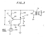
- FIG.3 is a circuit diagram showing the output signal converter according to a third background example.
- a diode D1 is used as the substitute for the third transistor Q13 in the output signal circuit shown in FIG.2 .
- simplification of a circuit is allowable up to an extent that is obtainable by using a diode as a substitute of a transistor.
- FIG.4 is an explanatory diagram showing different wave forms, wherein FIG.4A shows a wave form of a sine wave as an input signal, FIG.4B shows an output wave form when amplified the sine wave signal shown in FIG.4A by using an amplifier constituted with semiconductor devices, FIG.4C shows an output wave form when amplified the sine wave shown in FIG.4A by using a conventional tube amplifier (an amplifier constituted with a plurality of vacuum tubes), and FIG.4D shows an output wave form when amplified the sine wave signal shown in FIG.4A by using the output signal converting circuit shown in FIG.2 .
- FIG.4A shows a wave form of a sine wave as an input signal
- FIG.4B shows an output wave form when amplified the sine wave signal shown in FIG.4A by using an amplifier constituted with semiconductor devices
- FIG.4C shows an output wave form when amplified the sine wave shown in FIG.4A by using a conventional tube amplifier (an amplifier constituted with a plurality of vacuum tubes)
- the output wave form which substantially-truly presents the sine wave to be input is obtainable by using the amplifier containing semiconductor devices
- the output wave form specifically produced by the tube amplifier is obtainable when using the conventional tube amplifier as shown in FIG.4C .
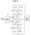
- FIG.5 is a circuit diagram showing the constitution of the output signal converter according to a fourth example.
- a push-pull amplifier is constituted with two vacuum tubes VA11 and VA12 in the output signal converter.
- two circuits each using a current mirror shown in FIG.2 are provided symmetrically at both upper and lower sites, each cathodes of the two vacuum tubes VA11 and VA12 are connected and a node thereof is connected to the ground via resistance R24.
- push-pull type power amplification is an output system which separates sound signals produced by a preamplifier into positive and negative signals by using a phase inverter PI, amplifying the positive side signals at an upper circuit (i.e. a circuit containing Q21, Q22, Q23, etc.) provided with the vacuum tube VA11, amplifying the negative side signals at a lower circuit (i.e. a circuit containing Q24, Q25, Q26, etc.) provided with vacuum tube VA12, and composing such signals at the output transformer TR and outputting them through the speaker SP.
- an upper circuit i.e. a circuit containing Q21, Q22, Q23, etc.
- a lower circuit i.e. a circuit containing Q24, Q25, Q26, etc.
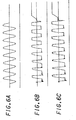
- FIG.6 shows a wave form showing the output property of the push-pull type amplifier shown in FIG.5 , wherein FIG.6A shows a sine wave as an input signal, FIG.6B shows an output wave form when applying the sine wave shown in FIG.6A into an amplifier constituted with four vacuum tubes, namely a conventional push-pull type tube amplifier, and FIG.6C shows an output wave form when applying the sine wave shown in FIG.6A into the amplifier shown in FIG.5 .
- FIG.7 is a circuit diagram showing the constitution of the output signal converter according to a fifth background example. As shown in FIG.7 , an output signal converter 7 is installed at the output side of a tube amplifier 5 containing just one vacuum tube and amplify and/or attenuate output signals with keeping the output property of the tube amplifier 5.
- the output signal converter 7 is constituted with a transformer 1 provided at the output side of the tube amplifier 5, a current amplifier 2 connected to a positive terminal at secondary side of the transformer 1, and a voltage amplifier 3 connected to the output side of the current amplifier 2 and of which output terminal being connected to a negative terminal at secondary side of the transformer 1. Further, a power circuit 6 is provided as an electric power supply for driving the tube amplifier 5 and the output signal converter 7. A speaker 4 connected to the rear side of the output signal converter 7, one of which terminals is connected to a node of the current amplifier 2 and the voltage amplifier 3, while the other terminal is connected to the ground.
- the output signal converter 7 can amplify or attenuate the level of the output signals to a desired level with maintaining the output property of the tube amplifier 5.
- output power value is proportional to a squared value of current amplification rate Ac at the current amplifier 2
- the output power value comes to a squared value of -3.16, that is 10, and therefore, ten times power can be given in this case.
- a purpose to attenuate the maximum output will be explained later in this specification.
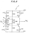
- FIG.8 is a circuit diagram showing a concrete constitution of the current amplifier 2 shown in FIG.7 .
- the current amplifier 2 is constituted with four transistors Q31 - Q34, a diode, a resistance, etc. and is arranged on a site between a power source +Vcc and a power source -Vee.
- an emitter of the transistor Q31 NPN-type
- an emitter of the transistor Q32 PNP-type
- a collector of the transistor Q31 is connected to the power source +Vcc via a diode D31 and a resistance R31.
- a collector of the transistor Q32 is connected to the power source -Vee via a diode D32 and a resistance R32.
- a connecting circuit which connects resistances R33, R35, R36 and R34 in series is connected, and a node of the resistances R33 and R35 is connected to a base of the transistor Q31, while a node of the resistances R36 and R34 is connected to a base of the transistor Q32.
- a collector of the transistor Q31 is connected to a base of the transistor Q33 (PNP-type), and similarly, a collector of the transistor Q32 is connected to a base of the transistor Q34 (NPN-type).
- a collector of the transistor Q33 and a collector of the transistor Q34 are connected, and an emitter of the transistor Q33 is connected to the power source +Vcc via a resistance R37, while an emitter of the transistor Q34 is connected to the power source -Vee via a resistance R38.
- a node of resistances R39 and R40 which is arranged on sites between each emitters of the transistors Q31 and Q32.
- a node of the resistance R35 and R36 is connected to the ground, and a node of a collector of the transistor Q33 and a collector of the transistor Q34 is designed as an output point of output current Iout.
- FIG.9 is a circuit diagram showing a concrete constitution of the voltage amplifier 3.
- the voltage amplifier 3 is constituted with four transistors Q41 - Q44 and a plurality of resistances and is connected to a site between the power sources +Vcc and -Vee to be actuated.
- a connecting circuit connecting resistances R41, R42, R43 and R44 in series is arranged, wherein a node of the resistance R41 and the resistance R42 is branched to two systems, one of the branches is connected to a base of the transistor Q41 (NPN-type), while the other branch is connected to the power source -Vee via a resistance R45.
- a node of the resistance R43 and the resistance R44 is branched into two systems, and one of the branches is connected to a base of the transistor Q42 (PNP-type), while the other is connected to the power source +Vcc via a resistance R46.
- a collector of the transistor Q41 is connected to the power source +Vcc, and an emitter is connected to a base of the transistor Q43 (NPN-type).
- a collector of the transistor Q42 is connected to the power source -Vee, and an emitter is connected to a base of the transistor Q44 (PNP-type).
- a collector of the transistor Q43 is connected to the power source +Vcc, a collector of the transistor Q44 is connected to the power source -Vee, and each emitters of the transistors Q43 and Q44 are connected via microresistances R47 and R48.
- a node of the resistance R42 and the resistance R43 is provided as an input point for voltage, that is a terminal voltage Vsp of the speaker 4 shown in FIG.7
- a node of the resistance R47 and the resistance R48 is provided as an output point for voltage, that is -Vin.
- Ir ⁇ 32 il + Ib
- Ir ⁇ 31 iu + Ib
- the resistances R39 and R40 and the two diodes D31 and D32 are factors to be used for stabilising the performance of the circuits.
- an input voltage in the voltage amplifier 3 is a voltage Vsp to be impressed into the speaker 4 (see FIG. 7 ), and an output voltage is Vin.
- a series connecting circuit containing the resistances R41 and R45 is arranged on a site between the positive power source +Vcc and negative power source -Vee so that a voltage at the node of the resistance R41 and R45 comes to a value being separated based on the value of such resistances.
- a voltage at the node of the resistances R41 and R45 comes +1.2 V, and this voltage is to be impressed into the base of the transistor Q41. Further, taking into consideration a fact that parallel resistance of the resistances R41 and R45 comes approximately 100 ⁇ and the resistance R42 is 100 ⁇ , a signal of which input voltage Vsp being attenuated to a 1/2 value is given to the node of the resistances R41 and R45, that is the base of the transistor Q41. Since the transistors Q41 and Q43 each independently perform as an emitter follower, a signal given to the base of transistor Q41 is to be output as an output voltage Vin. Namely, output voltage Vin becomes 1/2 value of input voltage VSP, and it will be understood that voltage amplification rate is 1/2.
- the output power can be four times increased.
- output power can be attenuated if setting the current amplification rate Ac to a value less than 1, and it gets the value closer to zero.
- the output of the tube amplifier 5 constituted by containing less number of vacuum tubes can be amplified by means of using semiconductor devices therein, such as a transistor, with maintaining the output property as obtainable by using tube amplifiers, and it is possible to obtain the output property which is substantially same as the one obtainable by using high power tube amplifiers.
- semiconductor devices therein such as a transistor
- the output signal converter it is also possible to attenuate the power of the tube amplifier 5.
- an object to attenuate output signals as described above is explained.
- Taking an example for an electronic guitar it is often intentionally done to distort output sound of the electronic guitar in order to create a feeling of presence and dynamism during a live concert. Therefore, even at the time of practising prior to the live concert, it is preferable to distort output sound as well as doing so at the live concert.
- it is required to output guitar sound at high sound volume in order to distort the output sound but it is difficult to do so in a studio for practice due to causing noise that is so troublesome to the neighbourhoods.
- the output signal converter shown in FIG.7 can attenuate the output produced by the tube amplifier 5 and can output the distorted-sound at low volume, it is very useful to use the output signal converter under such situation.
- the property of the tube amplifier can be either amplified or attenuated without causing the change in the property including an effect in power voltage fluctuation accompanying to load fluctuation of a tube amplifier.
- FIG.10 is an explanatory diagram showing a modified example for the output signal converter shown in FIG.7 , wherein the speaker 4 is connected in series in between an output terminal of the voltage amplifier 3 and an input terminal of the current amplifier 2, and a node of an output terminal of the current amplifier 2 and an input terminal of the voltage amplifier 3 is connected to one terminal located at the secondary side of the output transformer 1. And, it is also possible to obtain the same performance as the one obtainable by employing the output signal amplifying circuit shown in FIG.7 .
- the input impedance Z2 at output signal converter and the impedance at the speaker 4 will be understood as equal, and therefore, the output signals can be either amplified or attenuated with maintaining the output property obtainable by using the tube amplifier 5 which is provided at the front of the output transformer 1, as similar to the one according to the example shown in FIG.7 .
Landscapes
- Engineering & Computer Science (AREA)
- Power Engineering (AREA)
- Amplifiers (AREA)
Description
- The present invention is related to an output signal converter for connection to tube amplifiers which preferably is installed on the rear side of a tube amplifier and is capable of amplifying and attenuating output signals to convert them to a range of from high output to low output while maintaining advantages in output properties of tube amplifiers.
- In recent time, due to progress in the field of semiconductor technology, vacuum tube amplifiers for electronic musical instruments and audio systems being used as major in the past have been replaced by other type of amplifiers wherein semiconductor devices, such as transistors, are used. However, tube amplifiers have particular output properties which cannot be provided by amplifiers using semiconductor devices and are still acquiring persistent popularity so that a small number of tube amplifiers have been produced, sold and used yet.
- As it is well-known by the majority of peoples, because of such disadvantages of a vacuum tube, when comparing with semiconductor devices, as that it has shorter life longevity, is broken more easily and less reliable, bigger and inconvenient to install, heavier, produces greater heating value, is requiring high voltage power supply, and it costs higher, it is not practically possible to use vacuum tubes for amplifiers even though there are many requests which want to use vacuum tubes for amplifiers, and therefore, it is obliged in many cases to use the amplifiers constituted with semiconductor devices.
- For aiming at solving the problem as described above, many types of amplifiers which can mimetically articulate the output property of tube amplifiers by using semiconductor devices amplifier and counter electromotive force generated in a speaker affect the performance of a tube amplifier. Therefore, it will be understood that there is a limit in producing the output property obtainable in virtue of interactive relation by using an amplifier constituted with semiconductor devices. In fact, no amplifiers which can accurately imitate the output property of tube amplifiers have existed yet.
-
US-A-5635872 discloses an output signal converter for connection to a tube amplifier for converting an output signal from a tube amplifier, the output signal converter comprising an output transformer for connection to an output terminal of a tube amplifier and provided with first and second output terminals at the secondary side; wherein the output signal converter comprises a first semiconductor voltage amplifier connected to the first output terminal of the output transformer, wherein the first semiconductor voltage amplifier is arranged to amplify voltage input into the first semiconductor voltage amplifier; a first impedance connected in parallel to the first voltage amplifier; a second semiconductor voltage amplifier, wherein the second semiconductor voltage amplifier is arranged to amplify voltage input into the second semiconductor voltage amplifier, a second impedance connected in parallel to the second voltage amplifier; and a third impedance connected in series between the first and second voltage amplifiers. - According to the present invention there is provided an output signal converter for tube amplifiers as specified in claim 1.
- The preferred embodiment can provide an output signal converter for tube amplifiers in which output signals of predetermined power level can be obtained from those of the tube amplifiers containing a minimum number of vacuum tubes by converting the output signals by means of using semiconductor devices while maintaining output properties including transformer property and speaker property obtainable when using tube amplifiers.
- Now, a background example, not falling within the scope of the claims, will be described with reference to
FIG.1 . In the output signal converter according toFig. 1 , signals output from a vacuum tube VA1 flow through a first circuit C1. Besides, electric current proportioned to the current level flowing through the first circuit C1 flows into a second circuit C2 which is connected in parallel to the first circuit C1. The ratio of current value flown through the first circuit C1 versus current value flown through the second circuit C2 is determined depending upon the ratio of a first resistance R1 and a second resistance R2. For example, if R1 and R2 are equal in resistance value, current equivalent to the current flown through the first circuit C1 is supposed to flow through the second circuit C2. Consequently, electric current having amplified output signal from the vacuum tube VA1 to double level flows into the primary side of an output transformer TR, and the output property from the vacuum tube VA1 is maintained in the output signal. Therefore, by using one vacuum tube, it is allowed to obtain output signals which might be obtainable when using two vacuum tubes. Based on the embodiment as described above, particular output properties produced by using a vacuum tube can be obtained in large scale by means of using a minimum number of vacuum tubes, which have such disadvantages as that it has shorter longevity, broken easily, and inconvenient to install, and by using semiconductor devices for all other circuits. - Examples are described bellow with reference to the accompanying drawings, in which:
-
Fig. 1 is a circuit diagram showing the constitution of an output signal converter for tube amplifiers according to a first background example. -
Fig. 2 is a circuit diagram showing the constitution of the output signal converter for tube amplifiers according to a second background example. -
FIG.3 is a circuit diagram showing the constitution of the output signal converter for tube amplifiers according to a third embodiment background example. -
FIG.4 is a explanatory diagram showing output properties obtained when using the preferred output signal converters whereinFIG.4A shows a sine wave to be Input,FIG.4B shows a wave form of an output signal when input the sine wave into an amplifier constituted by using semiconductor devices only,FIG.4C shows a wave form of an output signal when input the sine wave into a tube amplifier, andFIG.4D shows a wave form of an output signal when input the sine wave into the circuit shown inFIG.2 . -
FIG.5 is a circuit diagram showing the constitution of the output signal converter for tube amplifiers according to a fourth background example, and it is an example of an application for a push-pull amplifier. -
FIG.6 is an explanatory diagram showing output properties when using the circuit shown inFIG.5 , whereinFIG.6A shows a sine wave to be input,FIG.6B shows a wave form of an output signal when input the sine wave into a push-pull amplifier containing four vacuum tubes, andFIG.6C shows a wave form of an output signal when input the sine wave into the circuit shown inFIG.5 . -
FIG.7 is a circuit diagram showing the constitution of the output signal converter for tube amplifiers according to a fifth background example. -
FIG.8 is a circuit diagram showing the concrete constitution of a current amplifier. -
FIG.9 is a circuit diagram showing the concrete constitution of a voltage amplifier. -
FIG.10 is a circuit diagram showing a modified example of the output signal converter for tube amplifiers shown inFIG.7 . -
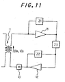
FIG.11 is a circuit diagram showing the constitution of the output signal converter for tube amplifiers according to a preferred embodiment of the present invention -
FIG.1 is a circuit diagram showing an output signal converter for tube amplifiers according to a first backgound example. With this output signal converter, it is possible to amplify output signals obtained from one vacuum tube VA1 maintaining its output property to thereby obtain output signals as if they are the ones having been obtained by using a plurality of vacuum tubes. - As shown in
FIG.1 , the output signal converter is provided on a site between a plate terminal of a vacuum tube VA1 and one of input terminals TRa of an output transformer TR and is constituted with a first circuit C1 which is formed by connecting a first resistance R1 and a first transistor Q1 in series and a second circuit C2 which is formed by connecting a second resistance R2 and a second transistor Q2 in series. - Namely, the terminal TRa is branched into two systems, and one of the systems (the first circuit C1) is connected to an emitter of the first transistor Q1 via the first resistance R1, and a collector of the transistor Q1 is connected to the plate terminal of the vacuum tube VA1. Whereas, the other system (the second circuit C2) is connected to an emitter of the second transistor Q2 via the second resistance R2, and a collector of the second transistor Q2 is connected to the ground. Further, a base of the first transistor Q1 is connected to the emitter of the second transistor Q2, and a base of the second transistor Q2 is connected to the plate terminal of the vacuum tube VA1.
- Now, detailed performance of the output signal converter as constituted above is explained below. Here, current flowing into the primary side of the transformer TR is defined as Iout, current flowing into the first circuit C1 is defined as Iin, voltage between the plate terminal of the vacuum tube VA1 and the input terminal TRa of the transformer TR is defined as V1, an impedance of the load side viewed from the transformer TR is defined as Zout, and an impedance of the load side viewed from the vacuum tube VA1 is defined as Zin. Here, the following equations (1) to (3) can be given:

- Provided that R1//R2 represents parallel resistance of the resistance R1 and the resistance R2 (R1 * R2 / R1 + R2).


- And, an equation (4) is obtained based on equations (2) and (3):

- Further, an equation, Iin = Vin/Zin, is applied into an equation (4), and an equation (1) is also applied into the equation (4), thereby the following equation (5) can be given:

- By modifying the equation (5) and developing R1//R2, the following equation (6) can be given:

- In the equation (6), when applying such condition as R1<<Zout and R2<<Zout, the following equation (7) can be given:

- From the equation (7), it will be understood that Zin and Zout are determined according to a ratio of the first resistance R1 and the second resistance R2. For example, when R1 = R2 is given, an equation, Zout = (1/2)Zin is lead, and the impedance comes to 1/2. Therefore, current output of the transformer TR becomes to a double value, which shows that output signals produced by the vacuum tube VA1 be amplified to a double level of the current output. In addition, current flowing into the second circuit C2, which is a circuit formed with the second resistance R2 and the second transistor Q2, comes to an equivalent value as the current flowing into the first circuit C1 so that Iout comes to a double value of Iin which apparently maintain the output property given by the vacuum tube VA1. As a result, it is allowed to obtain output signals, of which properties are the ones as if produced by two vacuum tubes, by using only one vacuum tube.
- Also, by appropriately changing a ratio of the first resistance R1 and the second resistance R2, it is possible to change current amplification rate. For example, if R2 = 2 * R1 is given, it is possible to triple the value of Iout relative to the value of Iin, and if R2 = (1/2) * R1 is given, it is possible to make a value of Iout to a 1.5 times value of Iin.
- As described above, according to the output signal converter shown in
FIG.1 , it is allowed to obtain output signals, of which property is similar to the one obtainable by using more than 1 vacuum tube, by using just one vacuum tube VA1, and therefore, it becomes feasible to reduce the number of vacuum tubes to be provided, which have such disadvantages as that it produces greater heating value, requires high voltage power supply, costs more, and has shorter longevity, to a minimum number. It is very advantageous to use the output signal converter according to the present example for amplifiers in use for guitars and audio systems. - Whereas, although a resistance R2 of which value being fixed is used in
FIG. 1 , when a variable resistance R2 is given, it is allowable to adjust the current value of Iout by controlling resistance value of the variable resistance to thereby allow to optionally control increase and reduction of output sound volume. Although sound volume control is normally operated at the input side, namely at the prior stage to the vacuum tube VA1 inFIG.1 , it is possible to adjust the sound volume with keeping the current Iin flowing into the vacuum tube VA1 at a substantially-fixed level by adopting a method to control resistance value of the second resistance R2, which allows to control the sound volume with keeping the output property produced by vacuum tubes. -
FIG.2 is a circuit diagram showing the constitution of the output signal converter for tube amplifiers according to a second background example. As shown inFIG.2 , the output signal converter is constituted of an output transformer TR, resistances R11, R12 and R3, and transistors Q11, Q12 and Q13. A connecting cable being connected to one of input terminals of the output transformer TR is branched into two systems, and one of the branches (a first circuit C1) is connected to a plate terminal of a vacuum tube VA1 via the first resistance R11 and, an emitter and a collector of the first transistor Q11, while the other branch (a second circuit C2) is connected to the ground via the second resistance R12, an emitter and a collector of the third transistor Q13, and further an emitter and a collector of the second transistor Q12. Further, a base of the first transistor Q11 and a. base of the third transistor Q13 are connected, and this node is further connected to a collector of the second transistor Q12. Therefore, a current mirror circuit is formed with the first transistor Q11 and the third transistor Q13. Whereas, a base of the second transistor Q12 is connected to the plate terminal of the vacuum tube VA1 via the resistance R3, and a speaker SP is connected to the output side of the output transformer TR. - In the example shown in
FIG.2 , because of formation of the current mirror circuit formed with the first transistor Q11 and the third transistor Q13, current directly imitating the property of the first transistor Q11, such as temperature characteristic, flow into the second circuit, and therefore, it is allowed to obtain output signals having fidelity to the output property produced by the vacuum tube VA1. -
FIG.3 is a circuit diagram showing the output signal converter according to a third background example. As shown inFIG.3 , a diode D1 is used as the substitute for the third transistor Q13 in the output signal circuit shown inFIG.2 . According to this type of constitution, although performance stability gets worse in comparison with that in the output signal converting circuit as shown inFIG.2 , simplification of a circuit is allowable up to an extent that is obtainable by using a diode as a substitute of a transistor. -
FIG.4 is an explanatory diagram showing different wave forms, whereinFIG.4A shows a wave form of a sine wave as an input signal,FIG.4B shows an output wave form when amplified the sine wave signal shown inFIG.4A by using an amplifier constituted with semiconductor devices,FIG.4C shows an output wave form when amplified the sine wave shown inFIG.4A by using a conventional tube amplifier (an amplifier constituted with a plurality of vacuum tubes), andFIG.4D shows an output wave form when amplified the sine wave signal shown inFIG.4A by using the output signal converting circuit shown inFIG.2 . As easily understood fromFIG.4B , contrary to that the output wave form which substantially-truly presents the sine wave to be input is obtainable by using the amplifier containing semiconductor devices, the output wave form specifically produced by the tube amplifier is obtainable when using the conventional tube amplifier as shown inFIG.4C . - When amplifying the sine wave shown in
FIG.4A by using the output signal converter shown inFIG.2 , it is possible to obtain output signals which are substantially equivalent to the output wave form obtainable by using a conventional tube amplifier as shown inFIG.4D , thus it will be understood that the output signal converter of the present invention is truly reproducing the output property given by a vacuum tube. -
FIG.5 is a circuit diagram showing the constitution of the output signal converter according to a fourth example. As shown inFIG.5 , a push-pull amplifier is constituted with two vacuum tubes VA11 and VA12 in the output signal converter. In brief, two circuits each using a current mirror shown inFIG.2 are provided symmetrically at both upper and lower sites, each cathodes of the two vacuum tubes VA11 and VA12 are connected and a node thereof is connected to the ground via resistance R24. - As it is well known, push-pull type power amplification is an output system which separates sound signals produced by a preamplifier into positive and negative signals by using a phase inverter PI, amplifying the positive side signals at an upper circuit (i.e. a circuit containing Q21, Q22, Q23, etc.) provided with the vacuum tube VA11, amplifying the negative side signals at a lower circuit (i.e. a circuit containing Q24, Q25, Q26, etc.) provided with vacuum tube VA12, and composing such signals at the output transformer TR and outputting them through the speaker SP. With the constitution as described above, as two vacuum tubes VA11 and VA12 are used therein, it is possible to obtain output property equivalent to the one obtainable by a push-pull type tube amplifier containing many vacuum tubes.
-
FIG.6 shows a wave form showing the output property of the push-pull type amplifier shown inFIG.5 , whereinFIG.6A shows a sine wave as an input signal,FIG.6B shows an output wave form when applying the sine wave shown inFIG.6A into an amplifier constituted with four vacuum tubes, namely a conventional push-pull type tube amplifier, andFIG.6C shows an output wave form when applying the sine wave shown inFIG.6A into the amplifier shown inFIG.5 . As easily understood fromFIGs.6B and 6C , it is confirmable that the output signal converter shown inFIG.5 can truly reproduce the output property produced by a vacuum tube, because it is demonstrated that substantially-equivalent wave forms are obtainable from the comparison of the wave forms obtainable by using a conventional push-pull type amplifier containing many vacuum tubes with the ones obtainable by using an amplifier containing a minimum number of vacuum tubes. -
FIG.7 is a circuit diagram showing the constitution of the output signal converter according to a fifth background example. As shown inFIG.7 , an output signal converter 7 is installed at the output side of atube amplifier 5 containing just one vacuum tube and amplify and/or attenuate output signals with keeping the output property of thetube amplifier 5. - The output signal converter 7 is constituted with a transformer 1 provided at the output side of the
tube amplifier 5, acurrent amplifier 2 connected to a positive terminal at secondary side of the transformer 1, and avoltage amplifier 3 connected to the output side of thecurrent amplifier 2 and of which output terminal being connected to a negative terminal at secondary side of the transformer 1. Further, a power circuit 6 is provided as an electric power supply for driving thetube amplifier 5 and the output signal converter 7. Aspeaker 4 connected to the rear side of the output signal converter 7, one of which terminals is connected to a node of thecurrent amplifier 2 and thevoltage amplifier 3, while the other terminal is connected to the ground. - And, in the output signal converter shown in
FIG.7 , there is a correlation provided for current amplification rate Ac of thecurrent amplifier 2 and voltage amplification rate Av of thevoltage amplifier 3 represented by an equation, Ac * Av = -1. Therefore, an impedance of the load side viewed from thetube amplifier 5 becomes equivalent to an impedance of the load side (i.e. the side of the speaker 4) viewed from the output signal converter 7, as if thetube amplifier 5 is directly connected to thespeaker 4. - Consequently, the output signal converter 7 can amplify or attenuate the level of the output signals to a desired level with maintaining the output property of the
tube amplifier 5. Namely, as output power value is proportional to a squared value of current amplification rate Ac at thecurrent amplifier 2, if conditions, Ac = -3.16 and Av = 0.316 are given, the output power value comes to a squared value of -3.16, that is 10, and therefore, ten times power can be given in this case. Or, contrary to this, when taking the value of current amplification rate closer to zero, it is possible to attenuate the maximum output with maintaining the output property of thetube amplifier 5. A purpose to attenuate the maximum output will be explained later in this specification. - Although the equation, Ac * Av = -1, is given in the explanation described above because the number of the
speaker 4 provided is just one, it is also possible to provide an equation, Ac * Av = -1 when twospeakers 4 are connected in series, or an equation, Ac * Av = -1/2, when twospeakers 4 are connected in parallel. Therefore, when describing in general, an equation, Ac * Av = - k (k is a constant) can be given. -
FIG.8 is a circuit diagram showing a concrete constitution of thecurrent amplifier 2 shown inFIG.7 . As shown inFIG.8 , thecurrent amplifier 2 is constituted with four transistors Q31 - Q34, a diode, a resistance, etc. and is arranged on a site between a power source +Vcc and a power source -Vee. - At the current input side, an emitter of the transistor Q31 (NPN-type) and an emitter of the transistor Q32 (PNP-type) are connected via resistances R39 and R40, and a collector of the transistor Q31 is connected to the power source +Vcc via a diode D31 and a resistance R31. Also, a collector of the transistor Q32 is connected to the power source -Vee via a diode D32 and a resistance R32. Whereas, between the power source +Vcc and the power source -Vee, a connecting circuit which connects resistances R33, R35, R36 and R34 in series is connected, and a node of the resistances R33 and R35 is connected to a base of the transistor Q31, while a node of the resistances R36 and R34 is connected to a base of the transistor Q32. Further, a collector of the transistor Q31 is connected to a base of the transistor Q33 (PNP-type), and similarly, a collector of the transistor Q32 is connected to a base of the transistor Q34 (NPN-type). And, a collector of the transistor Q33 and a collector of the transistor Q34 are connected, and an emitter of the transistor Q33 is connected to the power source +Vcc via a resistance R37, while an emitter of the transistor Q34 is connected to the power source -Vee via a resistance R38.
- And, it is designed to supply input current Iin to a node of resistances R39 and R40 which is arranged on sites between each emitters of the transistors Q31 and Q32. Whereas, a node of the resistance R35 and R36 is connected to the ground, and a node of a collector of the transistor Q33 and a collector of the transistor Q34 is designed as an output point of output current Iout.
-
FIG.9 is a circuit diagram showing a concrete constitution of thevoltage amplifier 3. As shown inFIG.9 , thevoltage amplifier 3 is constituted with four transistors Q41 - Q44 and a plurality of resistances and is connected to a site between the power sources +Vcc and -Vee to be actuated. Between the power sources +Vcc and -Vee, a connecting circuit connecting resistances R41, R42, R43 and R44 in series is arranged, wherein a node of the resistance R41 and the resistance R42 is branched to two systems, one of the branches is connected to a base of the transistor Q41 (NPN-type), while the other branch is connected to the power source -Vee via a resistance R45. Similarly, a node of the resistance R43 and the resistance R44 is branched into two systems, and one of the branches is connected to a base of the transistor Q42 (PNP-type), while the other is connected to the power source +Vcc via a resistance R46. - Further, a collector of the transistor Q41 is connected to the power source +Vcc, and an emitter is connected to a base of the transistor Q43 (NPN-type). Similarly, a collector of the transistor Q42 is connected to the power source -Vee, and an emitter is connected to a base of the transistor Q44 (PNP-type). In addition, a collector of the transistor Q43 is connected to the power source +Vcc, a collector of the transistor Q44 is connected to the power source -Vee, and each emitters of the transistors Q43 and Q44 are connected via microresistances R47 and R48. Further, a node of the resistance R42 and the resistance R43 is provided as an input point for voltage, that is a terminal voltage Vsp of the
speaker 4 shown inFIG.7 , and a node of the resistance R47 and the resistance R48 is provided as an output point for voltage, that is -Vin. - Now, performance of the output signal converting circuits shown in
FIGs. 7-9 are described in detail. In thecurrent amplifier 2 shown inFIG.8 , the two resistances R34 and R36 are arranged on sites between the power source -Vee and GND, and therefore, a voltage impressed to the base of the transistor Q32 comes to a value of [R34 / (R34 + R36)] * (-Vee). Due to impression of this voltage into the base of the transistor Q32, bias current Ib is flown to a site between the collector and the emitter of the transistor Q32, and input electric potential becomes to almost 0 V and this voltage is maintained irrespective of the start of input current flow. When voltage drop in the diode D31 and voltage drop between the base and the emitter of the transistor Q34 is same, voltage impressed to the resistances R32 and R38 are same too, so that a current Ir32 flowing into the resistance R32 and a current Ir38 flowing into the resistance R38 can be calculated according to the following equation:
- Similarly, if Ir37 = -Ir31 * R31 / R37, R31 = R32, R37 = R38, and k = R32 / R38 are given, Ir38 = -Ir32 * k, and Ir37 = -Ir31 * k are obtained. If input current I in is replaced by il-iu, wherein iu is current flowing in a direction to the resistance R39 and il is current flowing in a direction to the resistance R40, the following correlations are given:


- Then, an equation,

is obtained, and from which it will be understood that input current has been amplified. - Here, as examples for the constitutions of the circuits shown in
FIG.8 , the following assumptions can be made: - R31, R32 = 5Ω
- R33, R34 = 150Ω
- R35, R36 = 5Ω
- R37, R38 = 2.5Ω
- R39, R40 = 0.5Ω
- +Vcc = +20 V
- -Vee = -20 V
- According to the condition described above, R32/R38=2 is given, so it will be understandable that current amplification rate is a double value. The resistances R39 and R40 and the two diodes D31 and D32 are factors to be used for stabilising the performance of the circuits.
- Now, explanation is made with regard to the performance of the
voltage amplifier 3 shown inFIG.9 . In this figure, an input voltage in thevoltage amplifier 3 is a voltage Vsp to be impressed into the speaker 4 (seeFIG. 7 ), and an output voltage is Vin. As shown inFIG.9 , a series connecting circuit containing the resistances R41 and R45 is arranged on a site between the positive power source +Vcc and negative power source -Vee so that a voltage at the node of the resistance R41 and R45 comes to a value being separated based on the value of such resistances. Now, as concrete resistance values, the followings are provided: - R41, R44 = 189Ω
- R42, R43 = 100Ω
- R45, R46 = 213Ω
- +Vcc = +20 V
- -Vee = -20 V
- Then, a voltage at the node of the resistances R41 and R45 comes +1.2 V, and this voltage is to be impressed into the base of the transistor Q41. Further, taking into consideration a fact that parallel resistance of the resistances R41 and R45 comes approximately 100Ω and the resistance R42 is 100Ω, a signal of which input voltage Vsp being attenuated to a 1/2 value is given to the node of the resistances R41 and R45, that is the base of the transistor Q41. Since the transistors Q41 and Q43 each independently perform as an emitter follower, a signal given to the base of transistor Q41 is to be output as an output voltage Vin. Namely, output voltage Vin becomes 1/2 value of input voltage VSP, and it will be understood that voltage amplification rate is 1/2. With regard to the circuit shown on the lower part of the drawing which is constituted with the transistors Q42, Q44, etc., since there is difference in the circuit from the one shown on the upper part only in their polarity, and since it performs in the same manner as described above, no explanation on the circuit shall be made.
- As described above, it is allowable to constitute the
current amplifier 2 having a current amplification rate Ac of 2 and thevoltage amplifier 3 having a voltage amplification rate of 1/2, and since output voltage power supply produced by an output signal converting circuit equipped with suchcurrent amplifier 2 andsuch voltage amplifier 3 can be either amplified or attenuated proportionally to a squared value of the current amplification rate Ac, the output power can be four times increased. Whereas, output power can be attenuated if setting the current amplification rate Ac to a value less than 1, and it gets the value closer to zero. And, if thecurrent amplifier 2 and thevoltage amplifier 3 are connected with each other as shown inFIG.7 , a correlation of Ac * Av = -1 can be obtained so that the impedance of the load side viewed from thetube amplifier 5 gets equal to the impedance in case of directly connecting thespeaker 4 to thetube amplifier 5, while the impedance of the power side viewed from thespeaker 4 gets equal to the impedance in case of directly installing thetube amplifier 5 to thespeaker 4. Consequently, output property obtained from thetube amplifier 5 is directly amplified by the output signal converter 7 and then supplied to thespeaker 4, and therefore, it becomes possible to obtain the output property which is substantially same to the one obtainable by using either high power or low power vacuum tubes. - As described above, in the output signal converter shown in
FIG.7 , the output of thetube amplifier 5 constituted by containing less number of vacuum tubes can be amplified by means of using semiconductor devices therein, such as a transistor, with maintaining the output property as obtainable by using tube amplifiers, and it is possible to obtain the output property which is substantially same as the one obtainable by using high power tube amplifiers. In this way, it becomes possible to constitute a high power tube amplifier by using a minimum number of vacuum tubes which have such disadvantages as that it has shorter longevity, produces greater heating value, requires higher voltage power supply, and is more costly, and this type of amplifiers will be extremely advantageous for producing amplifiers in use for electronic guitar and audio system. In addition, there is. further advantage in the output signal converter according to the present example that it can reproduce the output property truly similar to the one obtainable by using the tube amplifiers, contrary to the output property obtainable by using the conventional amplifiers constituted by using semiconductor devices only, which is just imitating the output property of the tube amplifiers. - In the output signal converter according to this example, it is also possible to attenuate the power of the
tube amplifier 5. Now, an object to attenuate output signals as described above is explained. Taking an example for an electronic guitar, it is often intentionally done to distort output sound of the electronic guitar in order to create a feeling of presence and dynamism during a live concert. Therefore, even at the time of practising prior to the live concert, it is preferable to distort output sound as well as doing so at the live concert. However, it is required to output guitar sound at high sound volume in order to distort the output sound, but it is difficult to do so in a studio for practice due to causing noise that is so troublesome to the neighbourhoods. In such a case, since the output signal converter shown inFIG.7 can attenuate the output produced by thetube amplifier 5 and can output the distorted-sound at low volume, it is very useful to use the output signal converter under such situation. - Further, in the circuit shown in
FIG.7 , an example wherein a power supply for driving thetube amplifier 5 and a power supply for driving thecurrent amplifier 2 and thevoltage amplifier 3 are used in the same power circuit 6 is explained, however, it is also possible to constitute a circuit by arranging such power supplies each independently. In this case, the property of the tube amplifier can be either amplified or attenuated without causing the change in the property including an effect in power voltage fluctuation accompanying to load fluctuation of a tube amplifier. -
FIG.10 is an explanatory diagram showing a modified example for the output signal converter shown inFIG.7 , wherein thespeaker 4 is connected in series in between an output terminal of thevoltage amplifier 3 and an input terminal of thecurrent amplifier 2, and a node of an output terminal of thecurrent amplifier 2 and an input terminal of thevoltage amplifier 3 is connected to one terminal located at the secondary side of the output transformer 1. And, it is also possible to obtain the same performance as the one obtainable by employing the output signal amplifying circuit shown inFIG.7 . -
FIG.11 is a circuit diagram showing the constitution of the output signal converter according to a preferred embodiment of the present invention, and this output signal converter is constituted by containing first andsecond voltage amplifiers coefficient multiplier 13. Namely, thefirst voltage amplifier 11, a load Z3, thesecond voltage amplifier 12 and m-times coefficient multiplier 13 are connected in series at the secondary side of the output transformer 1, and a load Z1 is arranged in parallel to thefirst voltage amplifier 11, while a load Z2 is arranged in parallel to thesecond voltage amplifier 12. If an input current at the secondary side of the output transformer 1 is given as Iin and an input voltage is given as Vin, the following equation (9) can be given:
- According to the equation described above, an input impedance Zin can be given from the following equation (10):

- If a condition, Zin = Z2 is given, a correlation, m * (Z1 / Z3) = -1 is required to be given, and when the load Z3 is the
speaker 4, the voltage Vsp at both terminals of thespeaker 4 shall be given according to the following equation (11) :
- : Then, an amplification rate is given from an equation, Vsp / Vin, and the value obtained from this equation gets equal to -1/m. If m = 0.316 is given, Z1 = -1 and Z3 = 0.316 are then given. Since an output level is proportional to a squared value of 1/m, an equation, (1/0.316) * (1/0.316) = 10 is given, so that 10 times output can be obtainable. Further, as described above, since Zin = Z2 and Z2 is the
speaker 4, the input impedance Z2 at output signal converter and the impedance at thespeaker 4 will be understood as equal, and therefore, the output signals can be either amplified or attenuated with maintaining the output property obtainable by using thetube amplifier 5 which is provided at the front of the output transformer 1, as similar to the one according to the example shown inFIG.7 . - While the invention has been particularly shown and described with reference to a preferred embodiment thereof, it will be understood by those skilled in the art that various changes in form and details may be made therein without departing from the scope of the invention.
Claims (2)
- An output signal converter for connection to a tube amplifier for converting an output signal from a tube amplifier, the output signal converter comprising:an output transformer (1) for connection to an output terminal of a tube amplifier and provided with first and second output terminals at the secondary side;wherein the output signal converter comprises:a first semiconductor voltage amplifier (11) connected to the first output terminal of the output transformer (1), wherein the first semiconductor voltage amplifier is arranged to amplify voltage input into the first semiconductor voltage amplifier (11);a first impedance (Z1) connected in parallel to the first voltage amplifier (11);a coefficient multiplier (13) which is connected to the second output terminal of the output transformer (1);a second semiconductor voltage amplifier (12) connected to the coefficient multiplier (13), wherein the second semiconductor voltage amplifier is arranged to amplify voltage input into the second semiconductor voltage amplifier (12);a second impedance (Z2) connected in parallel to the second voltage amplifier (12); anda third impedance (Z3) connected in series between the first (11) and second (12) voltage amplifiers;wherein the coefficient multiplier (13) is arranged to multiply an input voltage by a factor of m, m being a coefficient of the coefficient multiplier (13);wherein the first output terminal of the output transformer (1), the first semiconductor voltage amplifier (11), the third impedance (Z3), the second semiconductor voltage amplifier (12), the coefficient multiplier (13) and the second output terminal of the output transformer (1) are connected in series and in this order, such that if an input current at the secondary side of the output transformer (1) is given as Iin and an input voltage is given as Vin, the following equation can be given:
 wherein the second impedance (Z2) is an impedance of a speaker.
 - An output signal converter according to claim 1, wherein an input impedance Zin can be given from the following equation:

Applications Claiming Priority (4)
| Application Number | Priority Date | Filing Date | Title |
|---|---|---|---|
| JP34872997A JP3539856B2 (en) | 1997-12-04 | 1997-12-04 | Output signal converter for vacuum tube amplifier |
| JP19903898A JP3662116B2 (en) | 1998-07-14 | 1998-07-14 | Output signal amplifier for vacuum tube amplifier |
| EP03019830A EP1372260B1 (en) | 1997-12-04 | 1998-12-04 | Output signal converter for tube amplifiers |
| EP98309973A EP0923194B1 (en) | 1997-12-04 | 1998-12-04 | Output signal converter for tube amplifiers |
Related Parent Applications (3)
| Application Number | Title | Priority Date | Filing Date |
|---|---|---|---|
| EP03019830A Division EP1372260B1 (en) | 1997-12-04 | 1998-12-04 | Output signal converter for tube amplifiers |
| EP98309973.0 Division | 1998-12-04 | ||
| EP03019830.3 Division | 2003-09-01 |
Publications (2)
| Publication Number | Publication Date |
|---|---|
| EP1732212A1 EP1732212A1 (en) | 2006-12-13 |
| EP1732212B1 true EP1732212B1 (en) | 2012-02-01 |
Family
ID=26511310
Family Applications (3)
| Application Number | Title | Priority Date | Filing Date |
|---|---|---|---|
| EP98309973A Expired - Lifetime EP0923194B1 (en) | 1997-12-04 | 1998-12-04 | Output signal converter for tube amplifiers |
| EP06019450A Expired - Lifetime EP1732212B1 (en) | 1997-12-04 | 1998-12-04 | Output signal converter for tube amplifiers |
| EP03019830A Expired - Lifetime EP1372260B1 (en) | 1997-12-04 | 1998-12-04 | Output signal converter for tube amplifiers |
Family Applications Before (1)
| Application Number | Title | Priority Date | Filing Date |
|---|---|---|---|
| EP98309973A Expired - Lifetime EP0923194B1 (en) | 1997-12-04 | 1998-12-04 | Output signal converter for tube amplifiers |
Family Applications After (1)
| Application Number | Title | Priority Date | Filing Date |
|---|---|---|---|
| EP03019830A Expired - Lifetime EP1372260B1 (en) | 1997-12-04 | 1998-12-04 | Output signal converter for tube amplifiers |
Country Status (3)
| Country | Link |
|---|---|
| US (2) | US6175271B1 (en) |
| EP (3) | EP0923194B1 (en) |
| DE (2) | DE69834617T2 (en) |
Families Citing this family (7)
| Publication number | Priority date | Publication date | Assignee | Title |
|---|---|---|---|---|
| US6175271B1 (en) | 1997-12-04 | 2001-01-16 | Korg Inc. | Output signal converter for tube amplifiers |
| US20020048379A1 (en) * | 2000-10-23 | 2002-04-25 | Gunnar Flentje | Guitar amplifier with volume control |
| US20020052665A1 (en) * | 2000-11-01 | 2002-05-02 | Memran Louis I. | Utilizing vacuum tubes in computer audio circuitry |
| US7932777B1 (en) * | 2003-03-24 | 2011-04-26 | Zipfel Jr George Gustave | Switching amplifier for driving reactive loads |
| WO2008062748A1 (en) * | 2006-11-20 | 2008-05-29 | Panasonic Corporation | Signal processing device and signal processing method |
| JPWO2017145241A1 (en) * | 2016-02-22 | 2018-09-27 | 健 赤石 | Amplifier output circuit |
| US10938364B2 (en) * | 2019-06-27 | 2021-03-02 | Echowell Electronic Co., Ltd. | Vacuum tube subwoofer extraction circuit system |
Family Cites Families (23)
| Publication number | Priority date | Publication date | Assignee | Title |
|---|---|---|---|---|
| US3566236A (en) * | 1968-10-17 | 1971-02-23 | William Z Johnson | Amplifier output stage coupling |
| JPS56158509A (en) * | 1980-05-12 | 1981-12-07 | Masaki Yoshimura | Audio power amplifier |
| US4439742A (en) | 1981-09-04 | 1984-03-27 | Peavey Electronics Corp. | Circuit for simulating vacuum tube compression in transistor amplifiers |
| US4937874A (en) | 1986-07-02 | 1990-06-26 | Pittman R Aspen | Emulated guitar loudspeaker |
| US5133014A (en) | 1990-01-18 | 1992-07-21 | Pritchard Eric K | Semiconductor emulation of tube amplifiers |
| US4809336A (en) | 1987-03-23 | 1989-02-28 | Pritchard Eric K | Semiconductor amplifier with tube amplifier characteristics |
| US5734725A (en) * | 1987-03-23 | 1998-03-31 | Pritchard; Eric K. | Tube emulator amplifier system |
| US5636284A (en) | 1987-03-23 | 1997-06-03 | Pritchard; Eric K. | Solid state emulation of vacuum tube audio power amplifiers |
| US5434536A (en) | 1987-03-23 | 1995-07-18 | Pritchard; Eric K. | Semiconductor emulation of vacuum tubes |
| US4995084A (en) | 1987-03-23 | 1991-02-19 | Pritchard Eric K | Semiconductor emulation of tube amplifiers |
| US5032796A (en) | 1989-12-19 | 1991-07-16 | St. Louis Music, Inc. | Solid state amplifier simulating vacuum tube distortion characteristics |
| US5131044A (en) | 1990-06-13 | 1992-07-14 | Peavey Electronics Corporation | Amplifier circuitry with mode compensation and selectable gain and frequency response in pre and post distortion circuits |
| US5805713A (en) | 1992-07-20 | 1998-09-08 | Pritchard; Eric K. | Solid state circuit for emulating push-pull tube amplifier |
| US5422599A (en) * | 1993-07-16 | 1995-06-06 | Larsen; Lawrence E. | Single-ended, transformer coupled audio amplifiers |
| US5619578A (en) | 1994-01-10 | 1997-04-08 | Peavey Electronics Corporation | Multi-stage solid state amplifier that emulates tube distortion |
| US5524055A (en) | 1994-01-18 | 1996-06-04 | Peavey Electronics Corporation | Solid state circuit for emulating tube compression effect |
| US5635872A (en) * | 1995-11-16 | 1997-06-03 | Maven Peal Instruments, Inc. | Variable control of electronic power supplies |
| US5668499A (en) | 1996-01-16 | 1997-09-16 | Peavey Electronics Corporation | Tube type power amplifier with distortion control |
| JP2909019B2 (en) * | 1996-03-25 | 1999-06-23 | 有限会社ザンデンオーディオシステム | Vacuum tube amplifier circuit for audio |
| US5789689A (en) | 1997-01-17 | 1998-08-04 | Doidic; Michel | Tube modeling programmable digital guitar amplification system |
| US6175271B1 (en) * | 1997-12-04 | 2001-01-16 | Korg Inc. | Output signal converter for tube amplifiers |
| JP3662116B2 (en) | 1998-07-14 | 2005-06-22 | 株式会社コルグ | Output signal amplifier for vacuum tube amplifier |
| JP3539856B2 (en) | 1997-12-04 | 2004-07-07 | 株式会社コルグ | Output signal converter for vacuum tube amplifier |
-
1998
- 1998-11-24 US US09/200,102 patent/US6175271B1/en not_active Expired - Lifetime
- 1998-12-04 DE DE69834617T patent/DE69834617T2/en not_active Expired - Fee Related
- 1998-12-04 EP EP98309973A patent/EP0923194B1/en not_active Expired - Lifetime
- 1998-12-04 DE DE69838349T patent/DE69838349T2/en not_active Expired - Lifetime
- 1998-12-04 EP EP06019450A patent/EP1732212B1/en not_active Expired - Lifetime
- 1998-12-04 EP EP03019830A patent/EP1372260B1/en not_active Expired - Lifetime
-
2000
- 2000-10-25 US US09/695,940 patent/US6229387B1/en not_active Expired - Lifetime
Also Published As
| Publication number | Publication date |
|---|---|
| DE69838349D1 (en) | 2007-10-11 |
| EP1372260A3 (en) | 2004-06-16 |
| US6229387B1 (en) | 2001-05-08 |
| EP1372260B1 (en) | 2007-08-29 |
| DE69834617T2 (en) | 2007-05-03 |
| EP0923194A3 (en) | 2002-10-30 |
| DE69838349T2 (en) | 2008-05-21 |
| US6175271B1 (en) | 2001-01-16 |
| EP1372260A2 (en) | 2003-12-17 |
| EP1732212A1 (en) | 2006-12-13 |
| EP0923194A2 (en) | 1999-06-16 |
| EP0923194B1 (en) | 2006-05-24 |
| DE69834617D1 (en) | 2006-06-29 |
Similar Documents
| Publication | Publication Date | Title |
|---|---|---|
| US5424683A (en) | Differential amplification circuit wherein a DC level at an output terminal is automatically adjusted and a power amplifier wherein a BTL drive circuit is driven by a half wave | |
| US4439743A (en) | Biasing circuit for power amplifier | |
| US5636284A (en) | Solid state emulation of vacuum tube audio power amplifiers | |
| US6646508B1 (en) | Wide bandwidth, current sharing, MOSFET audio power amplifier with multiple feedback loops | |
| JP2891326B2 (en) | Multi-stage solid-state amplifier that reproduces electron tube distortion | |
| NL193076C (en) | Amplifier control chain. | |
| JP2614988B2 (en) | Solid state vacuum tube compression circuit | |
| US4644289A (en) | Variable power amplifier for audio frequency signals and method | |
| EP1732212A1 (en) | Output signal converter for tube amplifiers | |
| US4055818A (en) | Tone control circuit | |
| JPS59107699A (en) | Stereo reproducing device | |
| US6350943B1 (en) | Electric instrument amplifier | |
| US5734725A (en) | Tube emulator amplifier system | |
| US4507615A (en) | Non-linear amplifier systems | |
| KR900005872B1 (en) | amplifier | |
| EP0265763A2 (en) | Frequency response compensation circuit | |
| JP3662116B2 (en) | Output signal amplifier for vacuum tube amplifier | |
| JP4187827B2 (en) | Circuit device, semiconductor integrated circuit device including the same, and communication device including the same | |
| US5113144A (en) | Feed-back type emphasis circuit | |
| JP3850799B2 (en) | Circuit structure for providing exponential predistortion to adjustable amplifiers. | |
| US5450034A (en) | Reflected plate amplifier | |
| EP0198478A2 (en) | Amplifier circuit | |
| US5160897A (en) | Push-pull power amplifying circuit | |
| KR950000433B1 (en) | Main amp for multi-output of sound system | |
| JP2752829B2 (en) | Variable gain amplifier circuit |
Legal Events
| Date | Code | Title | Description |
|---|---|---|---|
| PUAI | Public reference made under article 153(3) epc to a published international application that has entered the european phase |
Free format text: ORIGINAL CODE: 0009012 |
|
| AC | Divisional application: reference to earlier application |
Ref document number: 1372260 Country of ref document: EP Kind code of ref document: P Ref document number: 0923194 Country of ref document: EP Kind code of ref document: P |
|
| AK | Designated contracting states |
Kind code of ref document: A1 Designated state(s): DE GB |
|
| AX | Request for extension of the european patent |
Extension state: AL LT LV MK RO SI |
|
| 17P | Request for examination filed |
Effective date: 20070212 |
|
| 17Q | First examination report despatched |
Effective date: 20070326 |
|
| AKX | Designation fees paid |
Designated state(s): DE GB |
|
| GRAP | Despatch of communication of intention to grant a patent |
Free format text: ORIGINAL CODE: EPIDOSNIGR1 |
|
| GRAS | Grant fee paid |
Free format text: ORIGINAL CODE: EPIDOSNIGR3 |
|
| GRAA | (expected) grant |
Free format text: ORIGINAL CODE: 0009210 |
|
| AC | Divisional application: reference to earlier application |
Ref document number: 1372260 Country of ref document: EP Kind code of ref document: P Ref document number: 0923194 Country of ref document: EP Kind code of ref document: P |
|
| AK | Designated contracting states |
Kind code of ref document: B1 Designated state(s): DE GB |
|
| REG | Reference to a national code |
Ref country code: GB Ref legal event code: FG4D |
|
| RIN2 | Information on inventor provided after grant (corrected) |
Inventor name: MITOMA, HIROFUMI Inventor name: MORI, YASUHIKO Inventor name: MIEDA, FUMIO |
|
| REG | Reference to a national code |
Ref country code: DE Ref legal event code: R096 Ref document number: 69842585 Country of ref document: DE Effective date: 20120329 |
|
| PLBE | No opposition filed within time limit |
Free format text: ORIGINAL CODE: 0009261 |
|
| STAA | Information on the status of an ep patent application or granted ep patent |
Free format text: STATUS: NO OPPOSITION FILED WITHIN TIME LIMIT |
|
| 26N | No opposition filed |
Effective date: 20121105 |
|
| REG | Reference to a national code |
Ref country code: DE Ref legal event code: R097 Ref document number: 69842585 Country of ref document: DE Effective date: 20121105 |
|
| PGFP | Annual fee paid to national office [announced via postgrant information from national office to epo] |
Ref country code: DE Payment date: 20171211 Year of fee payment: 20 |
|
| PGFP | Annual fee paid to national office [announced via postgrant information from national office to epo] |
Ref country code: GB Payment date: 20171221 Year of fee payment: 20 |
|
| REG | Reference to a national code |
Ref country code: DE Ref legal event code: R071 Ref document number: 69842585 Country of ref document: DE |
|
| REG | Reference to a national code |
Ref country code: GB Ref legal event code: PE20 Expiry date: 20181203 |
|
| PG25 | Lapsed in a contracting state [announced via postgrant information from national office to epo] |
Ref country code: GB Free format text: LAPSE BECAUSE OF EXPIRATION OF PROTECTION Effective date: 20181203 |