EP1725856B1 - Method and apparatus for the two-dimensional mapping of the electro-optical coefficient - Google Patents
Method and apparatus for the two-dimensional mapping of the electro-optical coefficient Download PDFInfo
- Publication number
- EP1725856B1 EP1725856B1 EP05719035A EP05719035A EP1725856B1 EP 1725856 B1 EP1725856 B1 EP 1725856B1 EP 05719035 A EP05719035 A EP 05719035A EP 05719035 A EP05719035 A EP 05719035A EP 1725856 B1 EP1725856 B1 EP 1725856B1
- Authority
- EP
- European Patent Office
- Prior art keywords
- mrow
- values
- electromagnetic beam
- electro
- dimensional
- Prior art date
- Legal status (The legal status is an assumption and is not a legal conclusion. Google has not performed a legal analysis and makes no representation as to the accuracy of the status listed.)
- Expired - Lifetime
Links
- 238000000034 method Methods 0.000 title claims abstract description 66
- 238000013507 mapping Methods 0.000 title claims abstract description 18
- 239000000463 material Substances 0.000 claims abstract description 47
- 230000005684 electric field Effects 0.000 claims abstract description 45
- 238000001514 detection method Methods 0.000 claims abstract description 14
- 230000001427 coherent effect Effects 0.000 claims abstract description 9
- 230000006798 recombination Effects 0.000 claims abstract description 5
- 238000005215 recombination Methods 0.000 claims abstract description 5
- 239000013078 crystal Substances 0.000 claims description 25
- 238000012545 processing Methods 0.000 claims description 17
- 238000005070 sampling Methods 0.000 claims description 16
- 239000012780 transparent material Substances 0.000 claims description 12
- 239000000835 fiber Substances 0.000 claims description 11
- 230000008569 process Effects 0.000 claims description 8
- 238000004364 calculation method Methods 0.000 claims description 7
- 238000001093 holography Methods 0.000 claims description 7
- 230000005670 electromagnetic radiation Effects 0.000 claims description 5
- 230000008878 coupling Effects 0.000 claims description 4
- 238000010168 coupling process Methods 0.000 claims description 4
- 238000005859 coupling reaction Methods 0.000 claims description 4
- 238000009472 formulation Methods 0.000 claims description 3
- 239000000203 mixture Substances 0.000 claims description 3
- 230000005540 biological transmission Effects 0.000 claims description 2
- 230000009466 transformation Effects 0.000 claims description 2
- 230000001131 transforming effect Effects 0.000 claims description 2
- 230000003287 optical effect Effects 0.000 description 20
- 230000005855 radiation Effects 0.000 description 12
- 230000000694 effects Effects 0.000 description 11
- 238000005259 measurement Methods 0.000 description 11
- 230000005693 optoelectronics Effects 0.000 description 9
- 238000004458 analytical method Methods 0.000 description 8
- 230000006399 behavior Effects 0.000 description 6
- GQYHUHYESMUTHG-UHFFFAOYSA-N lithium niobate Chemical compound [Li+].[O-][Nb](=O)=O GQYHUHYESMUTHG-UHFFFAOYSA-N 0.000 description 6
- 239000007788 liquid Substances 0.000 description 5
- 238000010586 diagram Methods 0.000 description 4
- XLYOFNOQVPJJNP-UHFFFAOYSA-N water Substances O XLYOFNOQVPJJNP-UHFFFAOYSA-N 0.000 description 4
- 238000004891 communication Methods 0.000 description 3
- 230000005333 ferromagnetic domain Effects 0.000 description 3
- 230000010363 phase shift Effects 0.000 description 3
- 239000010453 quartz Substances 0.000 description 3
- 230000004044 response Effects 0.000 description 3
- VYPSYNLAJGMNEJ-UHFFFAOYSA-N silicon dioxide Inorganic materials O=[Si]=O VYPSYNLAJGMNEJ-UHFFFAOYSA-N 0.000 description 3
- 230000005697 Pockels effect Effects 0.000 description 2
- 238000012512 characterization method Methods 0.000 description 2
- 150000002500 ions Chemical class 0.000 description 2
- 239000004973 liquid crystal related substance Substances 0.000 description 2
- 239000007787 solid Substances 0.000 description 2
- 239000002253 acid Substances 0.000 description 1
- 150000007513 acids Chemical class 0.000 description 1
- 230000009471 action Effects 0.000 description 1
- 238000013459 approach Methods 0.000 description 1
- 230000015572 biosynthetic process Effects 0.000 description 1
- 230000008859 change Effects 0.000 description 1
- 238000001311 chemical methods and process Methods 0.000 description 1
- 230000008021 deposition Effects 0.000 description 1
- 238000011161 development Methods 0.000 description 1
- 238000005516 engineering process Methods 0.000 description 1
- 238000012615 high-resolution technique Methods 0.000 description 1
- 238000003384 imaging method Methods 0.000 description 1
- 230000002452 interceptive effect Effects 0.000 description 1
- 238000005305 interferometry Methods 0.000 description 1
- 238000011835 investigation Methods 0.000 description 1
- 238000004519 manufacturing process Methods 0.000 description 1
- 238000000691 measurement method Methods 0.000 description 1
- 238000012986 modification Methods 0.000 description 1
- 230000004048 modification Effects 0.000 description 1
- 238000012544 monitoring process Methods 0.000 description 1
- 239000013307 optical fiber Substances 0.000 description 1
- 229940125730 polarisation modulator Drugs 0.000 description 1
- 238000011160 research Methods 0.000 description 1
- 230000006641 stabilisation Effects 0.000 description 1
- 230000003068 static effect Effects 0.000 description 1
- 238000004148 unit process Methods 0.000 description 1
Images




Classifications
-
- G—PHYSICS
- G01—MEASURING; TESTING
- G01N—INVESTIGATING OR ANALYSING MATERIALS BY DETERMINING THEIR CHEMICAL OR PHYSICAL PROPERTIES
- G01N21/00—Investigating or analysing materials by the use of optical means, i.e. using sub-millimetre waves, infrared, visible or ultraviolet light
- G01N21/17—Systems in which incident light is modified in accordance with the properties of the material investigated
- G01N21/41—Refractivity; Phase-affecting properties, e.g. optical path length
- G01N21/45—Refractivity; Phase-affecting properties, e.g. optical path length using interferometric methods; using Schlieren methods
- G01N21/453—Holographic interferometry
-
- G—PHYSICS
- G03—PHOTOGRAPHY; CINEMATOGRAPHY; ANALOGOUS TECHNIQUES USING WAVES OTHER THAN OPTICAL WAVES; ELECTROGRAPHY; HOLOGRAPHY
- G03H—HOLOGRAPHIC PROCESSES OR APPARATUS
- G03H1/00—Holographic processes or apparatus using light, infrared or ultraviolet waves for obtaining holograms or for obtaining an image from them; Details peculiar thereto
- G03H1/04—Processes or apparatus for producing holograms
- G03H1/0402—Recording geometries or arrangements
- G03H1/041—Optical element in the object space affecting the object beam, not otherwise provided for
-
- G—PHYSICS
- G03—PHOTOGRAPHY; CINEMATOGRAPHY; ANALOGOUS TECHNIQUES USING WAVES OTHER THAN OPTICAL WAVES; ELECTROGRAPHY; HOLOGRAPHY
- G03H—HOLOGRAPHIC PROCESSES OR APPARATUS
- G03H1/00—Holographic processes or apparatus using light, infrared or ultraviolet waves for obtaining holograms or for obtaining an image from them; Details peculiar thereto
- G03H1/04—Processes or apparatus for producing holograms
- G03H1/0443—Digital holography, i.e. recording holograms with digital recording means
-
- G—PHYSICS
- G03—PHOTOGRAPHY; CINEMATOGRAPHY; ANALOGOUS TECHNIQUES USING WAVES OTHER THAN OPTICAL WAVES; ELECTROGRAPHY; HOLOGRAPHY
- G03H—HOLOGRAPHIC PROCESSES OR APPARATUS
- G03H1/00—Holographic processes or apparatus using light, infrared or ultraviolet waves for obtaining holograms or for obtaining an image from them; Details peculiar thereto
- G03H1/04—Processes or apparatus for producing holograms
- G03H1/0443—Digital holography, i.e. recording holograms with digital recording means
- G03H2001/0452—Digital holography, i.e. recording holograms with digital recording means arranged to record an image of the object
-
- G—PHYSICS
- G03—PHOTOGRAPHY; CINEMATOGRAPHY; ANALOGOUS TECHNIQUES USING WAVES OTHER THAN OPTICAL WAVES; ELECTROGRAPHY; HOLOGRAPHY
- G03H—HOLOGRAPHIC PROCESSES OR APPARATUS
- G03H2210/00—Object characteristics
- G03H2210/10—Modulation characteristics, e.g. amplitude, phase, polarisation
- G03H2210/12—Phase modulating object, e.g. living cell
-
- G—PHYSICS
- G03—PHOTOGRAPHY; CINEMATOGRAPHY; ANALOGOUS TECHNIQUES USING WAVES OTHER THAN OPTICAL WAVES; ELECTROGRAPHY; HOLOGRAPHY
- G03H—HOLOGRAPHIC PROCESSES OR APPARATUS
- G03H2210/00—Object characteristics
- G03H2210/63—Environment affecting the recording, e.g. underwater
Definitions
- the present invention concerns a method for the two-dimensional mapping of the electro-optical properties of transparent objects, a cell to be used in such a method for the application of an electrical field to objects, and relevant apparatus.
- the present invention is concerned with a method for determining the electro-optical properties of transparent objects and for the two-dimensional mapping thereof.
- the method applies in particular to those objects and devices, for which one desires to know the uniformity of their response to an electrical field, and to those objects which present structures with different electro-optical structures and of which one desires to know the two-dimensional mapping.
- the invention concerns further a cell into which can be placed such transparent materials and is suited to create in them an electrical field according to the needs of the method of the invention.
- the invention concerns an apparatus which realises the method according to the invention, notably using the cell according to the invention.
- the ferroelectric polarisation of the crystal is inverted by means of a process called of alignment of the ferroelectric domains or "poling", induced by an external electrical field.
- a process generates inside the crystal micrometric or submicrometric structures distributed according to 1, 2 or 3 dimensions, which interact differently with the light radiation.
- phase variation induced by the crystal on the incident light both in rest conditions and under conditions of externally induced stresses, as for example an electrical field.
- the structure can be either one-dimensional or bi- or three-dimensional, the need of having at disposal measurement techniques for two- or multi-dimensional mapping of the phase response of the crystals, which have undergone engineering processes of ferromagnetic domains, is nowadays more and more felt. For the same reason, is today necessary a technique which allows the on-site monitoring of the formation of the ferroelectric structures.
- the methods used at present for measuring the electro-optical properties are of local type, concerning only a small area of the sample, and provide an average information in the analysed area.
- the electro-optical coefficient is measured by using an interferometer with two beams provided with perpendicular, linear polarisations: an electrical field applied to the sample to be analysed induces different phase shifts between the interfering beams.
- said transparent material to be analysed is a non-centre-symmetrical crystal.
- the dimension perpendicular to the surface of the material, of which one detects the two-dimensional electro-optical properties have thickness of less than 5 mm.
- the dimension perpendicular to the surface of the material, of which one detects the two-dimensional electro-optical properties have thickness of less than 0,5 mm.
- the algorithm of digital holography utilises the numerical calculation of the diffraction integral in the Fresnel approximation, according to the following steps:
- said p values are arranged externally to said array of V r values.
- said p values are arranged in a symmetrical way.
- said p values are arranged in a non-symmetrical way.
- said number V e of values is inversely proportional to the desired pixel size to be obtained for the reconstructed image.
- each holographic image sampling interval is not equal or less than a certain threshold, the number of values p added to the digitised hologram array is increased and the second step is carried out again.
- said threshold is a function of the signal-to-noise ratio of the holographic image.
- an apparatus for measuring and two-dimensional mapping of the electro-optical properties of transparent materials comprising:
- the electromagnetic beam is let from the source in a single-mode, polarisation-maintaining fibre through the fibre coupling system.
- the electromagnetic beam is directed towards the Reflective Grating Interferometer in such a way that at least a part of it crosses the cell.
- the electromagnetic beam is emitted form an end of the single-mode, polarisation-maintaining fibre towards a parabolic mirror, which directs said electromagnetic beam towards the Reflective Grating Interferometer, in such a way that a part of the beam crosses the material in the cell and another part arrives undisturbed at the interferometric system.
- the parabolic mirror is placed at a distance from the end of the single-mode, polarisation-maintaining fibre such that the electromagnetic beam is collimated and expanded to dimensions which are comparable to those of the material.
- the Reflective Grating Interferometer (5) comprises a wave front division interferometer.
- the Reflective Grating Interferometer comprise a flat mirror mounted on adjustable supports on which impacts the part of the electromagnetic beam which has not crossed the material.
- the mirror is controlled so that the electromagnetic beam is redirected towards the diffraction grating.
- the processing electronic unit generates a signal suited to control said adjustable supports.
- the processing electronic unit generates signals suited to control the emission of the coherent light by said source and/or the electrical field applied to the material.
- the detection device of the electromagnetic beam is a two-dimensional array of detectors of electromagnetic radiation.
- the detection device is a CCD camera.
- the processing unit processes the data according to step E and/or G of the method according to the subject-matter of the invention.
- a coherent laser source 1 generates a laser beam, which is launched by means of the coupling means 2 in an optical single-mode fibre 3 which is suitable to maintain the polarisation.
- the cell 6 containing the sample is suitable to provide a high-quality optical access thanks to two quartz optical windows. Further, thanks to two seal chambers, it allows to inject a liquid electrode which therefore is in contact with both sides of the sample and assures a uniform electrical field on the sample.
- the liquid electrode is in general constituted by any conductive solution, for example by water with an ion concentration ranging from the average aqueduct concentration (about 180 mg/l) to that of a lithium-clorure-water solution (about 21200 mg/l).
- the object beam O undergoes a phase variation.
- the electrical field applied to the sample corresponds to a high-voltage signal produced by the amplifier 8 which is powered by a function generator.
- the system comprising generator and amplifier is controlled by an electronic processing unit 9, so as to predefine the type of field that one wishes to use for characterising the sample (constant, or linear-"ramp” signal or other type of signal), and in this way to adjust the emission of the source 1.
- the part O of the light beam crossing the sample arrives directly on the diffraction grating 5a and is diffracted towards the CCD camera 7, the part R of the light beam travelling undisturbed is first reflected on a flat mirror 5b and subsequently diffracted by the grating 5a on the CCD camera, which is in general constituted by a two-dimensional integrated array of radiation detectors.
- both beams superimpose on grating 5a in order to generate an interference image which carries the information of deformation of the phase variation undergone by the wave front of the light beam O crossing the sample 10 with respect to the wave front of the undisturbed beam R.
- the analysis of the wave front is made utilising a division-of-wave-front interferometer 5 wherein the recombination element 5a is a diffraction grating (see also, for example, Patent Request N° RM96A000178 filed on 19th March 1996 and the article of M. de Angelis et al., in Pure and Applied Optics, vol.24 (1995) 761-765 ).
- the digitised image detected by the device 7 is then stored in the processing electronic unit 9.
- the recorded interferometric image is analysed by means of an algorithm of digital holography, that is described in the following.
- This algorithm enables the two-dimensional reconstruction of the phase profile of the object beam which has undergone the variation (see also, for example, the article of S. De Nicola et al., Optics Letters, 26(13) 2001,974-876 and the Patent request N° RM2003A000398 deposed the 13th August 2003 ).
- figure 2 is reproduced a schematic representation of the cell that enables to apply an uniform electrical field and to assure the optical access to the material sample to be analysed.
- the configuration of the cell 6 is of "longitudinal" type, i.e. the electrical field is directed in the same propagation direction of the light needed to measure the phase variation induced in the crystal 10 under the effect of the electrical field.
- One of the sample utilised for verifying the working of the apparatus according to the invention is composed by a crystal of lithium niobate of the thickness of about 0,5 mm in which are present two bordering regions characterised by different electro-optical behaviours.
- the phase variation is mainly determined by the linear electro-optical and the piezoelectric effects.
- the sample could be thinner than the utilised one, since the apparatus according to the invention can appreciate phase variation, over optical paths, smaller than a micron.
- the sample is fixed by two rings 12 which are made of rubber or every other type of material that assures the seal.
- the rubber rings 12 allows to form two water seal chamber 14',14" wherein can be introduced a liquid electrode (generally a ion-rich water solution). In this manner, it is possible to apply to the sample an homogeneous electrical field.
- Quartz windows 11',11" enable a high-quality optical access, in the sense that they introduce deformations of negligible magnitude in the wave front of the radiation crossing the sample 10.
- the output cable of a high-voltage amplifier 8 is connected directly to the liquid contained in the seal chambers in order to provide the sample with the necessary voltage.
- the cell for use in the apparatus of the invention is therefore conceived so as to assure a high-quality optical access and at the same time to apply the necessary electrical field by means of liquid electrodes 15',15": this expedience allows to avoid the deposition of transparent, solid electrodes which are expensive and further are invasive since their removal is possible only by means of chemical processes based on acids.
- the tensor is not null only for crystals which are not centre-symmetric.
- the form of the tensor r ij can be deduced from the crystal's symmetry, that imposes which of the elements of the tensor are null and which relations exist between the remaining elements.
- the uniaxial crystal in the absence of applied electrical field, is placed in such a way that the optical axis is along the direction of light propagation and thus the applied electrical field as well.
- the application of the electrical field does not change the polarisation state of the light, rather it varies the phase of the light radiation crossing the sample.
- the interferometric signal is analysed by means of an algorithm called of digital holography and hereafter described.
- the interferometric image When detected by the image-detecting device (CCD camera), the interferometric image is transformed in a digitised interferogram, composed by a number of signal intensity values.
- the image is acquired, digitised and stored on an electronic processing device.
- the digitised image is called "digital hologram" and is described by an array H ( n ⁇ x , m ⁇ y ) of N ⁇ M values, obtained by the two-dimensional spatial sampling of the interferogram H(x,y), where n and m are integers, ⁇ x and ⁇ y are the sampling intervals along x and y axis respectively, and (N ⁇ ⁇ x)(M ⁇ ⁇ y) is the area of the acquired hologram image.
- the process of numerical reconstruction of the wave front of the object beam is based on two steps.
- the digitised hologram H(n,m) has to be multiplied by a digitised replica of the reference beam R(x,y), obtaining the following relation (5):
- the first two terms correspond to the zero order of diffraction, from the third and/or fourth terms being possile to deduce the image of the observed object.
- the second step of the propagation process consists in the reconstructing of the image from the plane in which the array of radiation detectors is placed to the plane in which the object is put. Such a reconstruction can be made through numerical calculation of the diffraction integral in the Fresnel approximation.
- ⁇ l ⁇ ⁇ ⁇ x , k ⁇ ⁇ ⁇ y Ae i ⁇ ⁇ d ⁇ l 2 ⁇ ⁇ ⁇ ⁇ 2 + k 2 ⁇ ⁇ ⁇ ⁇ 2 ⁇ DFT ⁇ R n ⁇ ⁇ , m ⁇ ⁇ ⁇ y ⁇ H n ⁇ ⁇ , m ⁇ ⁇ ⁇ y ⁇ e i ⁇ ⁇ d ⁇ n 2 ⁇ ⁇ ⁇ x 2 + m 2 ⁇ ⁇ ⁇ y 2 l , k
- ⁇ is the wavelength of the source
- A is a complex constant
- n, m, l, k are integers (-N / 2+1 ⁇ n) ⁇ N / 2 and -Ml2+1 ⁇ m,k ⁇ M / 2)
- DFT is the discrete Fourier transform, that can be calculated in a fast way making resort to the various algorithms of Fast Fourier Transform (FFT)
- ⁇ (l ⁇ x,k ⁇ y) arctan lm ⁇ ⁇ l ⁇ ⁇ ⁇ x , k ⁇ ⁇ ⁇ y Re ⁇ ⁇ l ⁇ ⁇ ⁇ x , k ⁇ ⁇ ⁇ y
- phase profile obtained by means of the analysis process of digital holography, for the above-mentioned lithium-niobate sample is shown in figure 3 , wherein the two orders of diffraction of the Fresnel integral are recognisable.
- the just described analysis process of the interferometric image enables the numerical reconstruction of the image on the crystal plane and the focusing of the object with a direct correspondence between phase map and sample's coordinates.
- the right-hand column of figure 5 shows the distribution of the values obtained for the given sample: the average value of the electro-optical parameter obtained for this sample is 10 pmN.
- the apparatus according to the invention can have configurations which are different from the one described above and can be realised with optical components without compromising or changing the apparatus itself.
- one has the possibility to determine with a single measurement operation the optical, two-dimensional behaviour of a sample of which one wishes to know the response to an applied electrical field.
- it can be extracted a two-dimensional mapping of the electro-optical behaviour of the sample using a single measure.
- the sample does not undergo any type of invasive treatment and is thus unaltered after the effectuated investigation.
- the invention sets itself in the technical field of optics and in the applicative one of the materials' characterisation and manufacture of optical and photonic equipments. Its principal uses are in the measurement of electro-optical properties and in the characterisation of materials utilised in optics and photonics as electro-optical modulators.
- the method and apparatus according to the invention enables the estimation of the uniformity of the electro-optical characteristics of a sample under the effect of an applied electrical field. They enable also to analyse complex structures in which are present zones of different nature as ferroelectric domains with different orientation in birefrangent crystals.
- the apparatus according to the invention presents particular characteristics of easiness of use, versatility and compactness.
Landscapes
- Physics & Mathematics (AREA)
- Health & Medical Sciences (AREA)
- Life Sciences & Earth Sciences (AREA)
- Chemical & Material Sciences (AREA)
- Analytical Chemistry (AREA)
- Biochemistry (AREA)
- General Health & Medical Sciences (AREA)
- General Physics & Mathematics (AREA)
- Immunology (AREA)
- Pathology (AREA)
- Investigating Or Analysing Materials By Optical Means (AREA)
- Immobilizing And Processing Of Enzymes And Microorganisms (AREA)
- Optical Integrated Circuits (AREA)
- Lasers (AREA)
Abstract
Description
- The present invention concerns a method for the two-dimensional mapping of the electro-optical properties of transparent objects, a cell to be used in such a method for the application of an electrical field to objects, and relevant apparatus.
- More particularly, the present invention is concerned with a method for determining the electro-optical properties of transparent objects and for the two-dimensional mapping thereof. The method applies in particular to those objects and devices, for which one desires to know the uniformity of their response to an electrical field, and to those objects which present structures with different electro-optical structures and of which one desires to know the two-dimensional mapping. The invention concerns further a cell into which can be placed such transparent materials and is suited to create in them an electrical field according to the needs of the method of the invention. Last but not least, the invention concerns an apparatus which realises the method according to the invention, notably using the cell according to the invention.
- There are materials, as for example crystals without centre of symmetry, in which it is present a birefringence induced by the linear electrical field, which is called linear electro-optic effect or Pockels effect; it is proportional to the electrical field and therefore to the applied voltage.
- The delay of a light beam crossing such crystals can be changed at will by means of an applied electrical field and this is the reason why such crystals are often used as phase modulators, polarisation modulators, in amplitude modulators, as optical switches and in general as optical and photonic devices (see A. Yariv "Quantum Electronics" Wiley Ed., New York 1988).
- During last years, a great effort has been done in the research in order to produce new crystals suitable to show a good electro-optical effect, and the development of such materials adds continuously new crystals to the list of those already existing; it is therefore extremely interesting to have at disposal high-resolution techniques, which are reliable and easy-to-use for studying of electro-optical properties of crystals.
- In a large number of applications, both in scientific and industrial field, a need exist to measure with enough accuracy electro-optical properties, notably the so-called electro-optical coefficient, of nonuniform structures, and therefore to have a multi-dimensional map of the structure under examination.
- For example, in crystals of photonic interest, the ferroelectric polarisation of the crystal is inverted by means of a process called of alignment of the ferroelectric domains or "poling", induced by an external electrical field. Such a process generates inside the crystal micrometric or submicrometric structures distributed according to 1, 2 or 3 dimensions, which interact differently with the light radiation. In this type of structure, it is crucial the knowledge of phase variation induced by the crystal on the incident light, both in rest conditions and under conditions of externally induced stresses, as for example an electrical field. Since the structure can be either one-dimensional or bi- or three-dimensional, the need of having at disposal measurement techniques for two- or multi-dimensional mapping of the phase response of the crystals, which have undergone engineering processes of ferromagnetic domains, is nowadays more and more felt. For the same reason, is today necessary a technique which allows the on-site monitoring of the formation of the ferroelectric structures.
- From now on, we will focalise on the linear electro-optical or Pockels effect, it should be however clear that what we will state will be also valid for the other electro-optical properties (for example, the Kerr or quadratic electro-optical effect, the piezoelectric effect or, better, the inverted piezoelectric effect: it deals with a variation in the shape and/or dimensions of the sample when is placed in an electrical field).
- The methods used at present for measuring the electro-optical properties are of local type, concerning only a small area of the sample, and provide an average information in the analysed area.
- Up to now, several techniques have been proposed for measuring the electro-optical coefficients in birefringence crystals. Some are polarimetric, as the Senarmont type (see in this concern P. C. Lemaire, and M. P. Georges, ; K. Chah, M. Aillerie, M. D. Fontana, and G. Malovichko, Optics Communication 176, (2000) 261-265), some others are interferometric, since they use interferometers of Michelson or Mach-Zehnder type. The former are simple experimental apparatuses, the latter requires the use of more complex apparatuses and are very sensitive to vibrations.
- During last years, many improvements have been done in the interferometric-type techniques, enabling the reach of high sensibilities in the measurements. It has been used for example a Michelson interferometer (P. Ney, A. Maillard, M. D. Fontana, and K. Polgàr, J. Opt. Soc. Am. B 17, (2000) 1158-1165), which includes an electro-optical modulator in one of the branches of the interferometer. With this apparatus, one is able to determine very small differences of optical path, by measuring the phase shift of the reference modulator which is needed to compensate for the phase shift caused by the application of the static electrical field of the crystal.
- It has been proposed recently (P. Delaye, and G. Roosen, Optics Communication 214, (2002) 199-206) a technique based on a Mach-Zehnder interferometer, which enables measurements having a good sensibility without any stabilisation of the apparatus, thanks to an innovative data processing system.
- Another interferometric method with signal modulation exists for precise measurements of electro-optical coefficients (J. A. de Toro, M. D. Serrano, A. Garcìa Cabañes, and J. M. Cabrera, Optics Communication 154 (1998) 23-27); a good accuracy is reached by obtaining the signal of first and second harmonic of the frequency modulation, while the phase is electronically varied along the two interference orders.
- Further, it has been developed a method (X. Yin, Q. Pan, W. Shi, and C. Fang, Applied Optics 41 (2002) 5929-5932) which is based on a Twyman-Green interferometer which uses the piezo-electric effect of a quartz crystal in order to compensate for the optical path changements caused by the electro-optical effect of the sample.
- According to another approach (J. Koo, C. Lee, J. H. Jang, K. No, and B. Bae, Applied Physics Letters 76 (2000) 2671-2673), the electro-optical coefficient is measured by using an interferometer with two beams provided with perpendicular, linear polarisations: an electrical field applied to the sample to be analysed induces different phase shifts between the interfering beams.
- The above-mentioned measurements are point measurements and are integrated on the sample thickness. As a consequence, an extension of such techniques to a two-dimensional mapping requires long measurement periods to disadvantage of the correlation between measures carried out at different times. These aspects make the carried out measurements operations slow, expensive and not much reliable.
- Moreover, for the application of the electrical field to the sample to be analysed, it is customary to deposit transparent solid electrodes which prove to be invasive and not easy to be realised unless one has specific and expensive equipments.
- In the article of Storrow G.M. et al. "An analysis of the optical properties of a single-element liquid crystal device", Pure and Applied Optics IOP Publishing UK, vol.7, no.6, November 1998(1998-11), pages 1411-1423, it is disclosed a method for phase imaging for measuring optical properties of an electrically controlled birefrangent liquid crystal at electrode edges, i.e. in the part of the material subjected to fringing fields. Such a method uses a Michelson interferometer and let the beam pass through the sample twice. It uses the phase-stepping interferometry technique, where three images have to be detected in order to retrieve the phase difference between the beam transmitted by the sample and the reference beam, each time for a specified value of the external voltage.
- In the article of De Angelis et al. "Interferometric analysis of a lithium niobate with engineering reversed domains", Proceedings of the SPIE SPIE-Int- Soc. Opt. Eng. USA, vol. 5144, 2003, pages 745-752, it is disclosed a method for measuring discontinuities of electro-optical properties in materials transparent to the electromagnetic radiation, using a reflective grating interferometer. The method comprises the acquisition of two images of a sample not subjected to any electrical field, one with the sample and one without the sample in the experimental set-up.
- It is an object of the present invention to provide a method for measuring the electro-optical coefficient of transparent materials, solving the above-mentioned drawbacks.
- It is further specific object of the present invention an apparatus for measuring the electro-optical properties of transparent materials solving the above-mentioned drawbacks.
- It is specific subject matter of this invention a method for measuring and two-dimensional mapping of the electro-optical properties of materials transparent to the electromagnetic radiation, the method using a Reflective Grating Interferometer wherein a substantially coherent and monochromatic electromagnetic beam is projected onto the transparent material to be analysed, which is subjected to an homogeneous electrical field, in such a way that the beam is enlarged as far as to have a two-dimensional cross section comparable with the dimensions of the material to be analysed, and dividing said electromagnetic beam in two parts, in such a way that one part crosses the material, the other part travels undisturbed, the two beams being recomposed on a diffraction grating representing the recombination element of the Reflective Grating Interferometer, the beam exiting from said Reflective Grating Interferometer being detected by means of a device suited to two-dimensionally detection of such beam, the method further comprising the following subsequent steps:
- E. obtaining, by means of an algorithm of digital holography, from the detected electromagnetic beam, which is representative of a two-dimensional image, the phase variation Δφ (x,y) of the electromagnetic beam which has crossed the material with respect to that of the undisturbed electromagnetic beam;
- F. for a number of P times, varying the applied electrical field value and repeating the preceding detection steps;
- G. calculating, for each pixel, the two-dimensional electro-optical parameter r' 13 (x, y) of the material under examination, using the formula:

- Preferably according to the invention, said transparent material to be analysed is a non-centre-symmetrical crystal.
- Preferably according to the invention, the dimension perpendicular to the surface of the material, of which one detects the two-dimensional electro-optical properties, have thickness of less than 5 mm.
- Preferably according to the invention, the dimension perpendicular to the surface of the material, of which one detects the two-dimensional electro-optical properties, have thickness of less than 0,5 mm.
- Preferably according to the invention, the algorithm of digital holography utilises the numerical calculation of the diffraction integral in the Fresnel approximation, according to the following steps:
- transforming the detected interferometric image into a digitised interferogram, composed by a number of Vr values of signal intensity, described by an array H(n·Δx,m·Ay) of N·M values, where n and m are integers, Δx and Δy are the sampling intervals along the x and y axis respectively and (N·Δx)(M·Δy) is the area of the acquired hologram;
- multiplying the digitised hologram H(n·Δx.m·Δy) by a digitised replica of the reference beam R(n·Δx,m·Δy), whereby obtaining the relation:

- reconstructing the image from the plane in which it has been detected to the plane in which the material to be analysed is put, by means of numerical calculation of the diffraction integral in the Fresnel approximation with the discrete formulation of the Fresnel integral expressed in terms of the Fourier transform, that is:

where λ is the wavelength of the source, A is a complex constant, n, m, l, k are integers (-N/2+1<n,l<N/2 e -M/2+1 <m,k<M/2), DFT is the discrete Fourier transform, Δx and Δy are the sampling intervals of the interferogram, d is the distance between the plane of the detection device and the observation plane, and, finally, Δξ and Δη represent the spatial sampling intervals in the observation plane and are defined by Δξ = λd/NΔx and Δη= λd/MΔy; - calculating the phase difference according to the formula:

- Preferably according to the invention, the method comprises a processing step of the digitised hologram array, and a step of reconstruction in the complex plane starting from the digitised hologram processed in the first step, in the reconstruction step being effectuated a discrete Fresnel transformation starting from an array of Ve values, comprising said Vr values of signal intensity values corresponding to as many elementary pixels of the holographic image, the pixel sizes being equal to the holographic image sampling intervals, as well as an integer number p = Ve - Vr > 0 of constant values equal to OS, corresponding to as many pixels of sizes equal to the ones of the others.
- Preferably according to the invention, said p constant values are null values (OS = 0).
- Preferably according to the invention, said p values are arranged externally to said array of Vr values.
- Preferably according to the invention, said p values are arranged in a symmetrical way.
- Preferably according to the invention, said p values are arranged in a non-symmetrical way.
- Preferably according to the invention, said number Ve of values is inversely proportional to the desired pixel size to be obtained for the reconstructed image.
- Preferably according to the invention, the digitised hologram is a square array of Vr = Nr · Mr values, each value corresponding to a square pixel of sizes Δx, Δy.
- Preferably according to the invention, the hologram reconstructed in the second step is represented by a square array of Ve = Ne ·Me values, each value corresponding to a square pixel of sizes Δξ= (λd/N e Δx) and Δη = (λd/MeΔy), λ being the wavelength of the wave beam striking the object of which the hologram is recorded, and d the distance between the detection device and the object of which the hologram is detected, Δξ and Δη being the reconstructed holographic image sampling intervals.
- Preferably according to the invention. Ne = (λdlΔx2), Me = (λd/Δy2), Δξ = Δx, Δη = Δy.
- Preferably according to the invention, after the second step, if each holographic image sampling interval is not equal or less than a certain threshold, the number of values p added to the digitised hologram array is increased and the second step is carried out again.
- Preferably according to the invention, said threshold is a function of the signal-to-noise ratio of the holographic image.
- It is specific further subject matter of the present invention an apparatus for measuring and two-dimensional mapping of the electro-optical properties of transparent materials, comprising:
- a source of coherent and single-mode electromagnetic beam,
- a system of transmission and projection of said beam,
- a Reflective Grating interferometer for the treatment of the projected electromagnetic beam,
- a device for detecting of the electromagnetic beam exiting from the interferometric system and a processing unit for processing the information relevant to the detected electromagnetic beam,
- a cell wherein the material to be analysed has to be placed, the cell and said material being crossable by at least a part of the projected electromagnetic beam, the cell being suited to crate an electrical field in the material,
- a diffraction grating on which impacts the part of the electromagnetic beam which has crossed the material,
- Preferably according to the invention, the electromagnetic beam is let from the source in a single-mode, polarisation-maintaining fibre through the fibre coupling system.
- Preferably according to the invention, the electromagnetic beam is directed towards the Reflective Grating Interferometer in such a way that at least a part of it crosses the cell.
- Preferably according to the invention, the electromagnetic beam is emitted form an end of the single-mode, polarisation-maintaining fibre towards a parabolic mirror, which directs said electromagnetic beam towards the Reflective Grating Interferometer, in such a way that a part of the beam crosses the material in the cell and another part arrives undisturbed at the interferometric system.
- Preferably according to the invention, the parabolic mirror is placed at a distance from the end of the single-mode, polarisation-maintaining fibre such that the electromagnetic beam is collimated and expanded to dimensions which are comparable to those of the material.
- Preferably according to the invention, the Reflective Grating Interferometer (5) comprises a wave front division interferometer.
- Preferably according to the invention, the Reflective Grating Interferometer comprise a flat mirror mounted on adjustable supports on which impacts the part of the electromagnetic beam which has not crossed the material.
- Preferably according to the invention, the mirror is controlled so that the electromagnetic beam is redirected towards the diffraction grating.
- Preferably according to the invention, the processing electronic unit generates a signal suited to control said adjustable supports.
- Preferably according to the invention, the processing electronic unit generates signals suited to control the emission of the coherent light by said source and/or the electrical field applied to the material.
- Preferably according to the invention, the detection device of the electromagnetic beam is a two-dimensional array of detectors of electromagnetic radiation.
- Preferably according to the invention, the detection device is a CCD camera.
- Preferably according to the invention, the processing unit processes the data according to step E and/or G of the method according to the subject-matter of the invention.
- The invention will be now described, by way of illustration and not by way of limitation, by particularly referring to the drawings of the enclosed Figures, in which:
-
Figure 1 shows a schematic representation of the apparatus according to the invention for the two-dimensional mapping of the electro-optical properties of samples of transparent materials; -
Figure 2 shows a schematic representation of the cell according to the invention; -
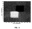
Figure 3 shows a diagram in which it is reproduced the phase map deformed by the electro-optical effect of a sample of transparent material, obtained by elaborating the interferometric signal; -
Figure 4 shows a diagram wherein it is reproduced the phase linear variation induced on the light radiation crossing the sample, in the event that the sample is nominally uniform in the electro-optical behaviour in the XY plane, as a function of the voltage applied to the sample; -
Figure 5 shows a diagram in which it is reproduced a two-dimensional mapping of the electro-optical properties of the sample relevant toFigure 4 ; -
Figure 6 shows a three-dimensional graph wherein it is plotted the two-dimensional mapping of the electro-optical properties of the sample relevant toFigures 4 and5 , treated beforehand. - The method described herein briefly comprises the following phases:
- a monochromatic, coherent light beam is produced, which is divided into two parts, a part crosses the sample whose electro-optical coefficient is to be measured (object beam O) and its phase is altered as a function of the electro-optical coefficient of the sample, the other part travels undisturbed (reference beam R) and provide the reference phase of the light radiation;
- the two beams are recomposed on a diffraction grating which represents the recombination element of the utilised interferometric system;
- by observing the interference signal, one deduces the phase variation, and therefore the wave front variation, of the radiation beam which has crossed the sample with respect to that of the undisturbed radiation; such a signal is recorded by an integrated, two-dimensional array of radiation detectors;
- such a phase variation is deduced for different values of the electrical field applied to the sample, afterwards one executes as many measurements as electrical field values are applied to the sample;
- knowing the applied voltage difference and the refraction index of the sample at the wavelength of the incident light, one deduces the contribution of the electro-optical effects of the material under examination by means of a two-dimensional mapping.
- For expository clarity, before going deeply into the matter of the analysis that leads to the calculation of the two-dimensional, electro-optical properties, it is illustrated an embodiment realising the apparatus which implements the method according to the Invention.
- With reference to
Figure 1 , all the parts which compose the apparatus according to a preferred embodiment are listed in the following: - 1 laser source,
- 2 system of fibre coupling,
- 3 single-mode, polarisation-maintaining fibre,
- 4 parabolic mirror,
- 5a diffraction grating,
- 5b flat mirror on stable and adjustable supports (tiltmeters),
- 6 cell for the sample to be analysed,
- 7 CCD camera for acquiring images,
- 8 signal generator and high-voltage amplifier,
- 9 electronic processing unit.
- A
coherent laser source 1 generates a laser beam, which is launched by means of the coupling means 2 in an optical single-mode fibre 3 which is suitable to maintain the polarisation. - The beam exits from the
optical fibre 3 with a highly diverging spherical wave front and is collimated by means of a parabolic mirror 4 (for example of the diameter of around 15 cm). - One part of the beam crosses the sample, the other travels undisturbed. The cell 6 containing the sample is suitable to provide a high-quality optical access thanks to two quartz optical windows. Further, thanks to two seal chambers, it allows to inject a liquid electrode which therefore is in contact with both sides of the sample and assures a uniform electrical field on the sample.
- The liquid electrode is in general constituted by any conductive solution, for example by water with an ion concentration ranging from the average aqueduct concentration (about 180 mg/l) to that of a lithium-clorure-water solution (about 21200 mg/l).
- When an electrical field is applied to the sample, the object beam O undergoes a phase variation.
- The electrical field applied to the sample corresponds to a high-voltage signal produced by the
amplifier 8 which is powered by a function generator. - The system comprising generator and amplifier is controlled by an
electronic processing unit 9, so as to predefine the type of field that one wishes to use for characterising the sample (constant, or linear-"ramp" signal or other type of signal), and in this way to adjust the emission of thesource 1. - The part O of the light beam crossing the sample arrives directly on the
diffraction grating 5a and is diffracted towards the CCD camera 7, the part R of the light beam travelling undisturbed is first reflected on aflat mirror 5b and subsequently diffracted by the grating 5a on the CCD camera, which is in general constituted by a two-dimensional integrated array of radiation detectors. - With a suitable choice of angles of incidence, both beams superimpose on grating 5a in order to generate an interference image which carries the information of deformation of the phase variation undergone by the wave front of the light beam O crossing the
sample 10 with respect to the wave front of the undisturbed beam R. - As it can be seen, the analysis of the wave front is made utilising a division-of-wave-
front interferometer 5 wherein therecombination element 5a is a diffraction grating (see also, for example, Patent Request N°RM96A000178 filed on 19th March 1996 - The digitised image detected by the device 7 is then stored in the processing
electronic unit 9. - The recorded interferometric image is analysed by means of an algorithm of digital holography, that is described in the following. This algorithm enables the two-dimensional reconstruction of the phase profile of the object beam which has undergone the variation (see also, for example, the article of S. De Nicola et al., Optics Letters, 26(13) 2001,974-876 and the Patent request N°
RM2003A000398 deposed the 13th August 2003 - In
figure 2 is reproduced a schematic representation of the cell that enables to apply an uniform electrical field and to assure the optical access to the material sample to be analysed. - The configuration of the cell 6 is of "longitudinal" type, i.e. the electrical field is directed in the same propagation direction of the light needed to measure the phase variation induced in the
crystal 10 under the effect of the electrical field. - One of the sample utilised for verifying the working of the apparatus according to the invention is composed by a crystal of lithium niobate of the thickness of about 0,5 mm in which are present two bordering regions characterised by different electro-optical behaviours.
- In the case of this sample, on which the electrical field is applied, the phase variation is mainly determined by the linear electro-optical and the piezoelectric effects.
- The sample could be thinner than the utilised one, since the apparatus according to the invention can appreciate phase variation, over optical paths, smaller than a micron.
- The sample is fixed by two
rings 12 which are made of rubber or every other type of material that assures the seal. The rubber rings 12 allows to form twowater seal chamber 14',14" wherein can be introduced a liquid electrode (generally a ion-rich water solution). In this manner, it is possible to apply to the sample an homogeneous electrical field. - Two
quartz windows 11',11" enable a high-quality optical access, in the sense that they introduce deformations of negligible magnitude in the wave front of the radiation crossing thesample 10. - The output cable of a high-
voltage amplifier 8 is connected directly to the liquid contained in the seal chambers in order to provide the sample with the necessary voltage. - The cell for use in the apparatus of the invention is therefore conceived so as to assure a high-quality optical access and at the same time to apply the necessary electrical field by means of
liquid electrodes 15',15": this expedience allows to avoid the deposition of transparent, solid electrodes which are expensive and further are invasive since their removal is possible only by means of chemical processes based on acids. - Coming now to the method of calculation of the electro-optical properties according to the invention, the effects of an electrical field on the propagation are properly expressed by the variations of the
refraction indexes 1/ni 2, with i = 1,...,6 and corresponding to the components x, y, z, xy, xz, yz, caused by the arbitrary electrical field E and defined by the following equation (1):
where the sum is made on the three components of the electrical field Ej and rij is the electro-optical tensor which has 18 independent elements and can be written as a 6 x 3 array. - The tensor is not null only for crystals which are not centre-symmetric.
- The form of the tensor rij can be deduced from the crystal's symmetry, that imposes which of the elements of the tensor are null and which relations exist between the remaining elements. In the case of the lithium niobate, for instance, the tensor is of the type given by the following expression (2):

- Where one sees that only 4 independent elements are necessary to describe the effect of electrical field.
- For example, to measure the term r13 one uses a "longitudinal" configuration: the uniaxial crystal, in the absence of applied electrical field, is placed in such a way that the optical axis is along the direction of light propagation and thus the applied electrical field as well. For such a type of alignment, the application of the electrical field does not change the polarisation state of the light, rather it varies the phase of the light radiation crossing the sample.
- Besides the variation of the refraction index due to the linear, electro-optical effect, there is a variation of the crystal thickness caused by the piezoelectric effect which depends on the components of the so-called "piezoelectric strain" tensor d33 in a way analogous to the dependence of the refraction index on the electro-optical tensor. In the end, the variation of the light radiation phase can be expressed by the following formula (3):

where with r'13 it is indicated the so-called electro-optical parameter corresponding to the overall contribution of the linear electro-optical effect and of the piezo-electric effect, r13 is the electro-optical coefficient expressed in m/V, n0 is the ordinary refraction index, V is the voltage difference in Volt and λ is the wavelength in metres. - In order to measure the r33 term, a so-called "transversal" configuration is used, in which the applied electrical field is perpendicular to the light propagation direction and the latter is perpendicular to the optical axis of the crystal. Other analogous configurations are possible in order to measure the remaining elements of the electro-optical tensor.
- In order to extract the phase profile of the wave front deformed by the sample due to the electro-optical effect, the interferometric signal is analysed by means of an algorithm called of digital holography and hereafter described.
- The interference image can be described in terms of two-dimensional distribution of intensity, according to the following formula (4):

where R, O, R* and O* are respectively the reference beam, the object beam and their complex conjugates. - When detected by the image-detecting device (CCD camera), the interferometric image is transformed in a digitised interferogram, composed by a number of signal intensity values.
- The image is acquired, digitised and stored on an electronic processing device. The digitised image is called "digital hologram" and is described by an array H(n·Δx,m·Δy) of N·M values, obtained by the two-dimensional spatial sampling of the interferogram H(x,y), where n and m are integers, Δx and Δy are the sampling intervals along x and y axis respectively, and (N·Δx)(M·Δy) is the area of the acquired hologram image.
- The process of numerical reconstruction of the wave front of the object beam is based on two steps.
- In the first step, the digitised hologram H(n,m) has to be multiplied by a digitised replica of the reference beam R(x,y), obtaining the following relation (5):

where the first two terms correspond to the zero order of diffraction, from the third and/or fourth terms being possile to deduce the image of the observed object. - The second step of the propagation process consists in the reconstructing of the image from the plane in which the array of radiation detectors is placed to the plane in which the object is put. Such a reconstruction can be made through numerical calculation of the diffraction integral in the Fresnel approximation.
- The advantages of such an approximation is based on the fact that its computation is simple and can be executed in a very rapid manner. In the case of the Fresnel approximation, the numerical reconstruction will be effectuated by means of a discrete formulation of the Fresnel integral expressed in terms of Fourier's transform, i.e. according to the following formula (6):

where λ is the wavelength of the source, A is a complex constant, n, m, l, k are integers (-N/2+1<n)<N/2 and -Ml2+ 1<m,k<M/2), DFT is the discrete Fourier transform, that can be calculated in a fast way making resort to the various algorithms of Fast Fourier Transform (FFT) reported in literature, Δx and Δy are the sampling intervals of the interferogram (therefore in the camera plane), d is the distance between the camera plane and the reconstruction plane, and finally Δξ and Δη represent the sampling spatial intervals in the reconstruction plane and are defined by: Δξ = λd/NΔx e Δη = λd/MΔy. - Once Ψ(lΔx,kΔy) has been calculated, it is possible to obtain both the intensity and the complex amplitude of the image. For our purposes, the phase is given by the following expression (7):

- The phase profile obtained by means of the analysis process of digital holography, for the above-mentioned lithium-niobate sample, is shown in
figure 3 , wherein the two orders of diffraction of the Fresnel integral are recognisable. - The just described analysis process of the interferometric image enables the numerical reconstruction of the image on the crystal plane and the focusing of the object with a direct correspondence between phase map and sample's coordinates.
- Other algorithms of analysis of interferometric images need the addition of lens in the experimental apparatus and relevant optical focusing, and do not assure the direct correspondence in dimensions of the sample and image.
- In
figure 4 the diagram of the phase variation induced on the light radiation crossing the lithium-niobate sample is reported, in the case in which the sample is nominally uniform, as a function of the voltage applied to the sample. - According to equation (3), the straight line best approximating experimental data has been plotted. Such a straight line has been deduced, in the specific example, using the least squares method that provides the best estimation of the straight line slope. From the latter and the knowledge of the ordinary refraction index under examination and of the light wavelength, one deduces the value of the electro-optical parameter r'13.
- The process just described that leads to the estimation of the electro-optical coefficient can be applied to any point individuated by the coordinates (x,y) or region of the phase map, shown in
figure 4 . In such a way, to each point in the plane xy of the sample under examination is associated an electro-optical coefficient's value. Such association is made contextually for all the points, thus by only one measure one obtains the electro-optical parameter of the sample. - Such result is shown in
figure 5 , wherein it is reported the two-dimensional mapping of the electro-optical parameter r'13 of the sample nominally uniform on the plane XY, on which the measurement procedure highlights different values of the electro-optical parameter itself, expressed in pmN (picometers/Volt). - The right-hand column of
figure 5 shows the distribution of the values obtained for the given sample: the average value of the electro-optical parameter obtained for this sample is 10 pmN. - The same procedure has been applied for an intentionally nonuniform sample, in which there is a structure with regions with different behaviour.
- The results is recognisable in
figure 6 , where it is reported the two-dimensional mapping of the electro-optical parameter of a lithium-niobate sample differently treated on two parts by means of the alignment or "poling" technique, with which two opposite ferromagnetic domains are created. The results show that in the sample are present two ferromagnetic domains oriented along opposite directions and having different behaviour under the action of the electrical field. - The apparatus according to the invention can have configurations which are different from the one described above and can be realised with optical components without compromising or changing the apparatus itself.
- To conclude, by means of the method and apparatus according to the invention, one has the possibility to determine with a single measurement operation the optical, two-dimensional behaviour of a sample of which one wishes to know the response to an applied electrical field. In particular, it can be extracted a two-dimensional mapping of the electro-optical behaviour of the sample using a single measure.
- Moreover, the sample does not undergo any type of invasive treatment and is thus unaltered after the effectuated investigation.
- The invention sets itself in the technical field of optics and in the applicative one of the materials' characterisation and manufacture of optical and photonic equipments. Its principal uses are in the measurement of electro-optical properties and in the characterisation of materials utilised in optics and photonics as electro-optical modulators.
- The method and apparatus according to the invention enables the estimation of the uniformity of the electro-optical characteristics of a sample under the effect of an applied electrical field. They enable also to analyse complex structures in which are present zones of different nature as ferroelectric domains with different orientation in birefrangent crystals.
- Further, the apparatus according to the invention presents particular characteristics of easiness of use, versatility and compactness.
- The preferred embodiments have been above described and some modifications of this invention have been suggested, but it should be understood that those skilled in the art can make variations and changes, without so departing from the related scope of protection, as defined by the following claims.
Claims (29)
- Method for measuring and two-dimensional mapping of the electro-optical properties of materials transparent to the electromagnetic radiation, the method using a Reflective Grating Interferometer (5) wherein a substantially coherent and monochromatic electromagnetic beam is projected onto the transparent material to be analysed, in such a way that the beam is enlarged as far as to have a two-dimensional cross section comparable with the dimensions of the material (10) to be analysed, and dividing said electromagnetic beam in two parts, in such a way that one part crosses the material (O), the other part travels undisturbed (R), the two beams (O,R) being recomposed on a diffraction grating (5a) representing the recombination element of the Reflective Grating Interferometer (5), the beam exiting from said Reflective Grating Interferometer (5) being detected by means of a device (7) suited to two-dimensionally detection of such beam characterised in that the transparent material to be analysed is subjected to an homogeneous electrical field, and the method further comprises the following subsequent steps:E. obtaining, by means of an algorithm of digital holography, from the detected electromagnetic beam, which is representative of a two-dimensional image, the phase variation Δφ (x,y) of the electromagnetic beam (O) which has crossed the material (10) with respect to that of the undisturbed electromagnetic beam (R);F. for a number of P times, varying the applied electrical field value and repeating the preceding detection steps;G. calculating, for each pixel, the two-dimensional electro-optical parameter r'13 (x, y) of the material (10) under examination, using the formula:where ΔΦ is the phase difference, V is the value of the voltage difference applied to the material (10) to be analysed, and n0 is the ordinary refraction index.

- Method according to claim 1, characterised in that said transparent material (10) to be analysed is a non-centre-symmetrical crystal.
- Method according to claim 1 or 2, characterised in that the dimension perpendicular to the surface of the material (10), of which one detects the two-dimensional electro-optical properties, have thickness of less than 5 mm.
- Method according to claim 3, characterised in that the dimension perpendicular to the surface of the material (10), of which one detects the two-dimensional electro-optical properties, have thickness of less than 0,5 mm.
- Method according to any claim 1 to 4, characterised in that the algorithm of digital holography utilises the numerical calculation of the diffraction integral in the Fresnel approximation, according to the following steps:- transforming the detected interferometric image into a digitised interferogram, composed by a number of Vr values of signal intensity, described by an array H(n·Δx,m·Δy) of N·M values, where n and m are integers, Δx and Δy are the sampling intervals along the x and y axis respectively and (N·Δx)(M·Δy) is the area of the acquired hologram;- multiplying the digitised hologram H(n·Δx,m·Δy) by a digitised replica of the reference beam R(n·Δx,m·Δy), whereby obtaining the relation:
 - reconstructing the image from the plane in which it has been detected to the plane in which the material to be analysed is put, by means of numerical calculation of the diffraction integral in the Fresnel approximation with the discrete formulation of the Fresnel integral expressed in terms of the Fourier transform, that is:where λ is the wavelength of the source, A is a complex constant, n, m, l, k are integers (-N/2+1<n,l<N/2 e -M/2+1<m,k<M/2), DFT is the discrete Fourier transform, Δx and Δy are the sampling intervals of the interferogram, d is the distance between the plane of the detection device and the observation plane, and, finally, Δξ and Δη represent the spatial sampling intervals in the observation plane and are defined by Δξ= λd/NΔx and Δη= λd/MΔy;
 - calculating the phase difference according to the formula:
- Method according to claim 5, characterised in that it comprises comprises a processing step of the digitised hologram array, and a step of reconstruction in the complex plane starting from the digitised hologram processed in the first step, in the reconstruction step being effectuated a discrete Fresnel transformation starting from an array of Ve values, comprising said Vr values of signal intensity values corresponding to as many elementary pixels of the holographic image, the pixel sizes being equal to the holographic image sampling intervals, as well as an integer number p = Ve - Vr > 0 of constant values equal to OS, corresponding to as many pixels of sizes equal to the ones of the others.
- Method according to claim 6, characterised in that said p constant values are null values (OS = 0).
- Method according to claim 6 or 7, characterised in that said p values are arranged externally to said array of Vr values.
- Method according to claim 8, characterised in that said p values are arranged in a symmetrical way.
- Method according to claim 9, characterised in that said p values are arranged in a non-symmetrical way.
- Method according to any preceding claim 6 to 10, characterised in that said number Ve of values is inversely proportional to the desired pixel size to be obtained for the reconstructed image.
- Method according to any preceding claim 6 to 11, characterised in that the digitised hologram is a square array of Vr = Nr·Mr values, each value corresponding to a square pixel of sizes Δx, Δy.
- Method according to claim 12, characterised in that the hologram reconstructed in the second step is represented by a square array of Ve = Ne·Me values, each value corresponding to a square pixel of sizes Δξ = (λdlNe Δx) and Δη = (λdlMe Δ y), λ being the wavelength of the wave beam striking the object of which the hologram is recorded, and d the distance between the detection device and the object of which the hologram is detected, Δξ and Δη being the reconstructed holographic image sampling intervals.
- Method according to claim 13, characterised in that Ne = (λd/Δx2), Me = (λd/Δy2), Δξ = Δx, Δη = Δy.
- Method according to any preceding claim 6 to 14, characterised in that, after the second step, if each holographic image sampling interval is not equal or less than a certain threshold, the number of values p added to the digitised hologram array is increased and the second step is carried out again.
- Method according to claim 15, characterised in that said threshold is a function of the signal-to-noise ratio of the holographic image.
- Apparatus for measuring and two-dimensional mapping of the electro-optical properties of transparent materials, comprising:- a source (1) of coherent and single-mode electromagnetic beam,- a system of transmission and projection (2,3,4) of said beam,- a Reflective Grating Interferometer (5) for the treatment of the projected electromagnetic beam,- a device (7) for detecting of the electromagnetic beam exiting from the interferometric system and a processing unit (9) for processing the information relevant to the detected electromagnetic beam,- a cell (6) wherein the material (10) to be analysed has to be placed, the cell (6) and said material (10) being crossable by at least a part of the projected electromagnetic beam, the cell (6) being suited to create an homogeneous electrical field in the material (10),- a diffraction grating (5a) on which impacts the part (O) of the electromagnetic beam which has crossed the material (10), wherebythe apparatus is adapted to implement the method according to any claim 1 to 16.
- Apparatus according to claim 17, characterised in that the electromagnetic beam is let from the source (1) in a single-mode, polarisation-maintaining fibre (3) through the fibre coupling system (2).
- Apparatus according to claim 17 or 18, characterised in that the electromagnetic beam is directed towards the Reflective Grating Interferometer (5) in such a way that at least a part of it crosses the cell (6).
- Apparatus according to claim 19, characterised in that the electromagnetic beam is emitted form an end of the single-mode, polarisation-maintaining fibre (3) towards a parabolic mirror (4), which directs said electromagnetic beam towards the Reflective Grating Interferometer (5), in such a way that a part (O) of the beam crosses the material (10) in the cell (6) and another part (R) arrives undisturbed at the interferometric system (5).
- Apparatus according to claim 20, characterised in that the parabolic mirror (4) is placed at a distance from the end (3') of the single-mode, polarisation-maintaining fibre (3) such that the electromagnetic beam is collimated and expanded to dimensions which are comparable to those of the material (10).
- Apparatus according to any claim 17 to 21, characterised in that the Reflective Grating Interferometer (5) comprises a wave front division interferometer.
- Apparatus according to any claim 19 to 22, characterised in that the Reflective Grating Interferometer (5) comprise a flat mirror (5b) mounted on adjustable supports on which impacts the part (R) of the electromagnetic beam which has not crossed the material (10).
- Apparatus according to claim 23, when depending on claim 26, characterised in that the mirror (5b) is controlled so that the electromagnetic beam is redirected towards the diffraction grating (5a).
- Apparatus according to claim 23 or 24, characterised in that the processing electronic unit (9) generates a signal suited to control said adjustable supports.
- Apparatus according to any claim 17 to 25, characterised in that the processing electronic unit (9) generates signals suited to control the emission of the coherent light by said source (1) and/or the electrical field applied to the material (10).
- Apparatus according to any claim 17 to 26, characterised in that the detection device (7) of the electromagnetic beam is a two-dimensional array of detectors of electromagnetic radiation.
- Apparatus according to claim 27, characterised in that the detection device (7) is a CCD camera,
- Apparatus according to any claim 17 to 28, characterised in that the processing unit (9) processes the data according to step E and/or G of the method according to any claim 1 to 16.
Applications Claiming Priority (2)
| Application Number | Priority Date | Filing Date | Title |
|---|---|---|---|
| IT000133A ITRM20040133A1 (en) | 2004-03-17 | 2004-03-17 | METHOD FOR THE TWO-DIMENSIONAL MAPPING OF THE ELECTRO-OPTICAL PROPERTIES OF OBJECTS, CELL TO BE USED IN SUCH METHOD FOR THE APPLICATION OF THE ELECTRIC FIELD TO OBJECTS, AND ITS APPARATUS. |
| PCT/IT2005/000135 WO2005088276A1 (en) | 2004-03-17 | 2005-03-11 | Method and apparatus for the two-dimensional mapping of the electro-optical coefficient |
Publications (2)
| Publication Number | Publication Date |
|---|---|
| EP1725856A1 EP1725856A1 (en) | 2006-11-29 |
| EP1725856B1 true EP1725856B1 (en) | 2009-06-17 |
Family
ID=34963043
Family Applications (1)
| Application Number | Title | Priority Date | Filing Date |
|---|---|---|---|
| EP05719035A Expired - Lifetime EP1725856B1 (en) | 2004-03-17 | 2005-03-11 | Method and apparatus for the two-dimensional mapping of the electro-optical coefficient |
Country Status (7)
| Country | Link |
|---|---|
| US (1) | US20070177158A1 (en) |
| EP (1) | EP1725856B1 (en) |
| JP (1) | JP2007529739A (en) |
| AT (1) | ATE434174T1 (en) |
| DE (1) | DE602005014946D1 (en) |
| IT (1) | ITRM20040133A1 (en) |
| WO (1) | WO2005088276A1 (en) |
Families Citing this family (2)
| Publication number | Priority date | Publication date | Assignee | Title |
|---|---|---|---|---|
| CN105424312A (en) * | 2015-11-25 | 2016-03-23 | 中国科学院长春光学精密机械与物理研究所 | Coaxial-paraboloid-based reflection type schlieren instrument optical system |
| KR102886247B1 (en) * | 2022-11-10 | 2025-11-17 | 한양대학교 산학협력단 | Optical Constant Measurement Devices and Methods for EUV Specimens |
Family Cites Families (5)
| Publication number | Priority date | Publication date | Assignee | Title |
|---|---|---|---|---|
| JP2649856B2 (en) * | 1990-04-13 | 1997-09-03 | 松下電器産業株式会社 | Nonlinear optical material |
| US6078392A (en) * | 1997-06-11 | 2000-06-20 | Lockheed Martin Energy Research Corp. | Direct-to-digital holography and holovision |
| US6525821B1 (en) * | 1997-06-11 | 2003-02-25 | Ut-Battelle, L.L.C. | Acquisition and replay systems for direct-to-digital holography and holovision |
| US6222632B1 (en) * | 1999-04-07 | 2001-04-24 | Luxtron Corporation | Polarization interferometer spectrometer with rotatable birefringent element |
| US6687010B1 (en) * | 1999-09-09 | 2004-02-03 | Olympus Corporation | Rapid depth scanning optical imaging device |
-
2004
- 2004-03-17 IT IT000133A patent/ITRM20040133A1/en unknown
-
2005
- 2005-03-11 AT AT05719035T patent/ATE434174T1/en not_active IP Right Cessation
- 2005-03-11 WO PCT/IT2005/000135 patent/WO2005088276A1/en not_active Ceased
- 2005-03-11 US US10/592,682 patent/US20070177158A1/en not_active Abandoned
- 2005-03-11 JP JP2007503499A patent/JP2007529739A/en active Pending
- 2005-03-11 EP EP05719035A patent/EP1725856B1/en not_active Expired - Lifetime
- 2005-03-11 DE DE602005014946T patent/DE602005014946D1/en not_active Expired - Lifetime
Also Published As
| Publication number | Publication date |
|---|---|
| WO2005088276A1 (en) | 2005-09-22 |
| ATE434174T1 (en) | 2009-07-15 |
| EP1725856A1 (en) | 2006-11-29 |
| JP2007529739A (en) | 2007-10-25 |
| DE602005014946D1 (en) | 2009-07-30 |
| US20070177158A1 (en) | 2007-08-02 |
| ITRM20040133A1 (en) | 2004-06-17 |
Similar Documents
| Publication | Publication Date | Title |
|---|---|---|
| US10883817B2 (en) | Method for full-field measurement using dynamic laser doppler imaging | |
| US6219142B1 (en) | Method and apparatus for determining wave characteristics from wave phenomena | |
| US11561081B2 (en) | Method for full-field measurement using dynamic laser doppler imaging | |
| Petrov et al. | Holography and phase retrieval in terahertz imaging | |
| Hotate | Application of synthesized coherence function to distributed optical sensing | |
| EP4407287A1 (en) | Polarimetric phase imaging | |
| De Angelis et al. | Liquid refractometer based on interferometric fringe projection | |
| Buse et al. | 3D imaging: wave front sensing utilizing a birefringent crystal | |
| US20070177158A1 (en) | Method and apparatus for the two-dimensional mapping of the electro-optical coefficient | |
| Barbosa | Holographic imaging with multimode, large free spectral range lasers in photorefractive sillenite crystals | |
| Trolinger | Ultrahigh resolution interferometry | |
| Zhao et al. | Digital speckle shearing interferometer using a liquid-crystal spatial light modulator | |
| Schake | Advanced theory of optical wave propagation and interferometric sensors for topography measurement | |
| Qu et al. | Digital holographic interferometry and the angular spectrum method applied to measuring the domain inversion in ferroelectric crystal | |
| JP3233723B2 (en) | Phase pattern difference discriminator | |
| Grilli et al. | Real-time phase-contrast analysis of domain switching in lithium niobate by digital holography | |
| De Nicola et al. | Characterization of microstructures in lithium niobate crystals by digital holography | |
| Oka et al. | Novel polarimetric technique exploring spatiotemporal birefringent response of an anti-ferroelectric liquid crystal cell | |
| Petrov et al. | Nonlinear interactions and scattering of space charge waves in sillenites | |
| RU2071047C1 (en) | Holographic method for determination of optical characteristics of transparent objects | |
| Wei-Juan et al. | Dynamic Phase-Mapping of Domain Nucleation in MgO: LiNbO3 Crystal by Digital Holographic Interferometry | |
| de Angelis et al. | Interferometric analysis of a lithium niobate with engineering reversed domains | |
| Vlad et al. | Real-time holographic interferometry in photorefractive BTO crystals using optical phase conjugation with a low power laser diode | |
| Lee et al. | Single-Shot Dual-Wavelength Digital Holography Using a Diffraction Grating | |
| Kikuta et al. | OPTICAL ENGINEERING FOR SENSING AND NANOTECHNOLOGY (ICOSN'01) 6-8 June 2001 Yokohama, Japan |
Legal Events
| Date | Code | Title | Description |
|---|---|---|---|
| PUAI | Public reference made under article 153(3) epc to a published international application that has entered the european phase |
Free format text: ORIGINAL CODE: 0009012 |
|
| 17P | Request for examination filed |
Effective date: 20060804 |
|
| AK | Designated contracting states |
Kind code of ref document: A1 Designated state(s): AT BE BG CH CY CZ DE DK EE ES FI FR GB GR HU IE IS IT LI LT LU MC NL PL PT RO SE SI SK TR |
|
| DAX | Request for extension of the european patent (deleted) | ||
| 17Q | First examination report despatched |
Effective date: 20070912 |
|
| GRAP | Despatch of communication of intention to grant a patent |
Free format text: ORIGINAL CODE: EPIDOSNIGR1 |
|
| GRAS | Grant fee paid |
Free format text: ORIGINAL CODE: EPIDOSNIGR3 |
|
| GRAA | (expected) grant |
Free format text: ORIGINAL CODE: 0009210 |
|
| AK | Designated contracting states |
Kind code of ref document: B1 Designated state(s): AT BE BG CH CY CZ DE DK EE ES FI FR GB GR HU IE IS IT LI LT LU MC NL PL PT RO SE SI SK TR |
|
| REG | Reference to a national code |
Ref country code: GB Ref legal event code: FG4D |
|
| REG | Reference to a national code |
Ref country code: CH Ref legal event code: EP |
|
| REG | Reference to a national code |
Ref country code: IE Ref legal event code: FG4D |
|
| REF | Corresponds to: |
Ref document number: 602005014946 Country of ref document: DE Date of ref document: 20090730 Kind code of ref document: P |
|
| PG25 | Lapsed in a contracting state [announced via postgrant information from national office to epo] |
Ref country code: FI Free format text: LAPSE BECAUSE OF FAILURE TO SUBMIT A TRANSLATION OF THE DESCRIPTION OR TO PAY THE FEE WITHIN THE PRESCRIBED TIME-LIMIT Effective date: 20090617 Ref country code: AT Free format text: LAPSE BECAUSE OF FAILURE TO SUBMIT A TRANSLATION OF THE DESCRIPTION OR TO PAY THE FEE WITHIN THE PRESCRIBED TIME-LIMIT Effective date: 20090617 Ref country code: LT Free format text: LAPSE BECAUSE OF FAILURE TO SUBMIT A TRANSLATION OF THE DESCRIPTION OR TO PAY THE FEE WITHIN THE PRESCRIBED TIME-LIMIT Effective date: 20090617 |
|
| PG25 | Lapsed in a contracting state [announced via postgrant information from national office to epo] |
Ref country code: SI Free format text: LAPSE BECAUSE OF FAILURE TO SUBMIT A TRANSLATION OF THE DESCRIPTION OR TO PAY THE FEE WITHIN THE PRESCRIBED TIME-LIMIT Effective date: 20090617 Ref country code: SE Free format text: LAPSE BECAUSE OF FAILURE TO SUBMIT A TRANSLATION OF THE DESCRIPTION OR TO PAY THE FEE WITHIN THE PRESCRIBED TIME-LIMIT Effective date: 20090917 Ref country code: PL Free format text: LAPSE BECAUSE OF FAILURE TO SUBMIT A TRANSLATION OF THE DESCRIPTION OR TO PAY THE FEE WITHIN THE PRESCRIBED TIME-LIMIT Effective date: 20090617 |
|
| NLV1 | Nl: lapsed or annulled due to failure to fulfill the requirements of art. 29p and 29m of the patents act | ||
| PG25 | Lapsed in a contracting state [announced via postgrant information from national office to epo] |
Ref country code: IS Free format text: LAPSE BECAUSE OF FAILURE TO SUBMIT A TRANSLATION OF THE DESCRIPTION OR TO PAY THE FEE WITHIN THE PRESCRIBED TIME-LIMIT Effective date: 20091017 Ref country code: RO Free format text: LAPSE BECAUSE OF FAILURE TO SUBMIT A TRANSLATION OF THE DESCRIPTION OR TO PAY THE FEE WITHIN THE PRESCRIBED TIME-LIMIT Effective date: 20090617 Ref country code: CZ Free format text: LAPSE BECAUSE OF FAILURE TO SUBMIT A TRANSLATION OF THE DESCRIPTION OR TO PAY THE FEE WITHIN THE PRESCRIBED TIME-LIMIT Effective date: 20090617 Ref country code: EE Free format text: LAPSE BECAUSE OF FAILURE TO SUBMIT A TRANSLATION OF THE DESCRIPTION OR TO PAY THE FEE WITHIN THE PRESCRIBED TIME-LIMIT Effective date: 20090617 Ref country code: ES Free format text: LAPSE BECAUSE OF FAILURE TO SUBMIT A TRANSLATION OF THE DESCRIPTION OR TO PAY THE FEE WITHIN THE PRESCRIBED TIME-LIMIT Effective date: 20090928 |
|
| PG25 | Lapsed in a contracting state [announced via postgrant information from national office to epo] |
Ref country code: BE Free format text: LAPSE BECAUSE OF FAILURE TO SUBMIT A TRANSLATION OF THE DESCRIPTION OR TO PAY THE FEE WITHIN THE PRESCRIBED TIME-LIMIT Effective date: 20090617 Ref country code: SK Free format text: LAPSE BECAUSE OF FAILURE TO SUBMIT A TRANSLATION OF THE DESCRIPTION OR TO PAY THE FEE WITHIN THE PRESCRIBED TIME-LIMIT Effective date: 20090617 Ref country code: NL Free format text: LAPSE BECAUSE OF FAILURE TO SUBMIT A TRANSLATION OF THE DESCRIPTION OR TO PAY THE FEE WITHIN THE PRESCRIBED TIME-LIMIT Effective date: 20090617 |
|
| PG25 | Lapsed in a contracting state [announced via postgrant information from national office to epo] |
Ref country code: BG Free format text: LAPSE BECAUSE OF FAILURE TO SUBMIT A TRANSLATION OF THE DESCRIPTION OR TO PAY THE FEE WITHIN THE PRESCRIBED TIME-LIMIT Effective date: 20090917 Ref country code: PT Free format text: LAPSE BECAUSE OF FAILURE TO SUBMIT A TRANSLATION OF THE DESCRIPTION OR TO PAY THE FEE WITHIN THE PRESCRIBED TIME-LIMIT Effective date: 20091017 |
|
| PLBE | No opposition filed within time limit |
Free format text: ORIGINAL CODE: 0009261 |
|
| STAA | Information on the status of an ep patent application or granted ep patent |
Free format text: STATUS: NO OPPOSITION FILED WITHIN TIME LIMIT |
|
| PG25 | Lapsed in a contracting state [announced via postgrant information from national office to epo] |
Ref country code: DK Free format text: LAPSE BECAUSE OF FAILURE TO SUBMIT A TRANSLATION OF THE DESCRIPTION OR TO PAY THE FEE WITHIN THE PRESCRIBED TIME-LIMIT Effective date: 20090617 |
|
| 26N | No opposition filed |
Effective date: 20100318 |
|
| PG25 | Lapsed in a contracting state [announced via postgrant information from national office to epo] |
Ref country code: GR Free format text: LAPSE BECAUSE OF FAILURE TO SUBMIT A TRANSLATION OF THE DESCRIPTION OR TO PAY THE FEE WITHIN THE PRESCRIBED TIME-LIMIT Effective date: 20090918 Ref country code: MC Free format text: LAPSE BECAUSE OF NON-PAYMENT OF DUE FEES Effective date: 20100331 |
|
| REG | Reference to a national code |
Ref country code: CH Ref legal event code: PL |
|
| PG25 | Lapsed in a contracting state [announced via postgrant information from national office to epo] |
Ref country code: IE Free format text: LAPSE BECAUSE OF NON-PAYMENT OF DUE FEES Effective date: 20100311 |
|
| PG25 | Lapsed in a contracting state [announced via postgrant information from national office to epo] |
Ref country code: CH Free format text: LAPSE BECAUSE OF NON-PAYMENT OF DUE FEES Effective date: 20100331 Ref country code: LI Free format text: LAPSE BECAUSE OF NON-PAYMENT OF DUE FEES Effective date: 20100331 |
|
| PGFP | Annual fee paid to national office [announced via postgrant information from national office to epo] |
Ref country code: IT Payment date: 20110305 Year of fee payment: 7 Ref country code: FR Payment date: 20110317 Year of fee payment: 7 |
|
| PGFP | Annual fee paid to national office [announced via postgrant information from national office to epo] |
Ref country code: GB Payment date: 20110309 Year of fee payment: 7 |
|
| PGFP | Annual fee paid to national office [announced via postgrant information from national office to epo] |
Ref country code: DE Payment date: 20110526 Year of fee payment: 7 |
|
| PG25 | Lapsed in a contracting state [announced via postgrant information from national office to epo] |
Ref country code: CY Free format text: LAPSE BECAUSE OF FAILURE TO SUBMIT A TRANSLATION OF THE DESCRIPTION OR TO PAY THE FEE WITHIN THE PRESCRIBED TIME-LIMIT Effective date: 20090617 |
|
| PG25 | Lapsed in a contracting state [announced via postgrant information from national office to epo] |
Ref country code: HU Free format text: LAPSE BECAUSE OF FAILURE TO SUBMIT A TRANSLATION OF THE DESCRIPTION OR TO PAY THE FEE WITHIN THE PRESCRIBED TIME-LIMIT Effective date: 20091218 Ref country code: LU Free format text: LAPSE BECAUSE OF NON-PAYMENT OF DUE FEES Effective date: 20100311 |
|
| PG25 | Lapsed in a contracting state [announced via postgrant information from national office to epo] |
Ref country code: TR Free format text: LAPSE BECAUSE OF FAILURE TO SUBMIT A TRANSLATION OF THE DESCRIPTION OR TO PAY THE FEE WITHIN THE PRESCRIBED TIME-LIMIT Effective date: 20090617 |
|
| GBPC | Gb: european patent ceased through non-payment of renewal fee |
Effective date: 20120311 |
|
| REG | Reference to a national code |
Ref country code: FR Ref legal event code: ST Effective date: 20121130 |
|
| PG25 | Lapsed in a contracting state [announced via postgrant information from national office to epo] |
Ref country code: FR Free format text: LAPSE BECAUSE OF NON-PAYMENT OF DUE FEES Effective date: 20120402 Ref country code: GB Free format text: LAPSE BECAUSE OF NON-PAYMENT OF DUE FEES Effective date: 20120311 |
|
| REG | Reference to a national code |
Ref country code: DE Ref legal event code: R119 Ref document number: 602005014946 Country of ref document: DE Effective date: 20121002 |
|
| PG25 | Lapsed in a contracting state [announced via postgrant information from national office to epo] |
Ref country code: IT Free format text: LAPSE BECAUSE OF NON-PAYMENT OF DUE FEES Effective date: 20120311 |
|
| PG25 | Lapsed in a contracting state [announced via postgrant information from national office to epo] |
Ref country code: DE Free format text: LAPSE BECAUSE OF NON-PAYMENT OF DUE FEES Effective date: 20121002 |