EP1724837A1 - Image sensor - Google Patents
Image sensor Download PDFInfo
- Publication number
- EP1724837A1 EP1724837A1 EP05253114A EP05253114A EP1724837A1 EP 1724837 A1 EP1724837 A1 EP 1724837A1 EP 05253114 A EP05253114 A EP 05253114A EP 05253114 A EP05253114 A EP 05253114A EP 1724837 A1 EP1724837 A1 EP 1724837A1
- Authority
- EP
- European Patent Office
- Prior art keywords
- image sensor
- column
- readout
- pixels
- additional
- Prior art date
- Legal status (The legal status is an assumption and is not a legal conclusion. Google has not performed a legal analysis and makes no representation as to the accuracy of the status listed.)
- Granted
Links
Images


Classifications
-
- H—ELECTRICITY
- H04—ELECTRIC COMMUNICATION TECHNIQUE
- H04N—PICTORIAL COMMUNICATION, e.g. TELEVISION
- H04N25/00—Circuitry of solid-state image sensors [SSIS]; Control thereof
-
- H—ELECTRICITY
- H04—ELECTRIC COMMUNICATION TECHNIQUE
- H04N—PICTORIAL COMMUNICATION, e.g. TELEVISION
- H04N25/00—Circuitry of solid-state image sensors [SSIS]; Control thereof
- H04N25/60—Noise processing, e.g. detecting, correcting, reducing or removing noise
- H04N25/68—Noise processing, e.g. detecting, correcting, reducing or removing noise applied to defects
-
- H—ELECTRICITY
- H10—SEMICONDUCTOR DEVICES; ELECTRIC SOLID-STATE DEVICES NOT OTHERWISE PROVIDED FOR
- H10F—INORGANIC SEMICONDUCTOR DEVICES SENSITIVE TO INFRARED RADIATION, LIGHT, ELECTROMAGNETIC RADIATION OF SHORTER WAVELENGTH OR CORPUSCULAR RADIATION
- H10F39/00—Integrated devices, or assemblies of multiple devices, comprising at least one element covered by group H10F30/00, e.g. radiation detectors comprising photodiode arrays
- H10F39/10—Integrated devices
- H10F39/12—Image sensors
- H10F39/18—Complementary metal-oxide-semiconductor [CMOS] image sensors; Photodiode array image sensors
-
- H—ELECTRICITY
- H10—SEMICONDUCTOR DEVICES; ELECTRIC SOLID-STATE DEVICES NOT OTHERWISE PROVIDED FOR
- H10F—INORGANIC SEMICONDUCTOR DEVICES SENSITIVE TO INFRARED RADIATION, LIGHT, ELECTROMAGNETIC RADIATION OF SHORTER WAVELENGTH OR CORPUSCULAR RADIATION
- H10F39/00—Integrated devices, or assemblies of multiple devices, comprising at least one element covered by group H10F30/00, e.g. radiation detectors comprising photodiode arrays
- H10F39/80—Constructional details of image sensors
- H10F39/802—Geometry or disposition of elements in pixels, e.g. address-lines or gate electrodes
-
- H—ELECTRICITY
- H10—SEMICONDUCTOR DEVICES; ELECTRIC SOLID-STATE DEVICES NOT OTHERWISE PROVIDED FOR
- H10F—INORGANIC SEMICONDUCTOR DEVICES SENSITIVE TO INFRARED RADIATION, LIGHT, ELECTROMAGNETIC RADIATION OF SHORTER WAVELENGTH OR CORPUSCULAR RADIATION
- H10F39/00—Integrated devices, or assemblies of multiple devices, comprising at least one element covered by group H10F30/00, e.g. radiation detectors comprising photodiode arrays
- H10F39/80—Constructional details of image sensors
- H10F39/803—Pixels having integrated switching, control, storage or amplification elements
Definitions
- the present invention relates to an image sensor and particularly to an image sensor with readout amplifier redundancy.
- Defects are caused during manufacture and are usually caused by dust particles obstructing the photolithography process. Resulting defects may be open circuit or short circuit connections.
- a defective pixel is usually the result.
- the defective pixel can be either ignored by the user or, if the defective pixel can be identified, corrected for by interpolating between neighbouring pixels.
- a series of pixels in the row or column may be defective, rather than a single pixel. In some cases, the entire row or column can be defective. Defects that disrupt the operation of more than one pixel are far more noticeable to a user and much harder to compensate for.
- a pixel array 100 has a matrix of pixels 102.
- Each column of pixels 102 in the pixel array 100 is connected by a common column bitline 104.
- Each row of pixels 102 is connected by a common row select 106.
- the row select 106 is activated (set to "high") by row drivers 108, the pixels 110 in that row are enabled for readout and the values of the pixels 102 are read out in parallel on to the column bitline 104 to readout amplifiers 110a, 110b, 100c.
- a horizontal scan 112 sends an "enable signal" along enable connection 114 to each readout amplifier 110 in turn.
- the amplified pixel value can then be read on an output bus 116.
- the readout amplifier 110 If the readout amplifier 110 is defective, the entire column of pixels cannot be readout correctly and, as such, a noticeable error occurs in the image.
- an image sensor having a plurality of pixels arranged in rows and columns to form a pixel array, each pixel column having a column bitline, the image sensor comprising a column readout for each column bitline and at least one additional column readout, wherein the at least one additional column readout may be selectively connected to one of the column bitlines.
- the at least one additional column readout may be selectively connected to one or more column bitlines by a first switch means.
- each column readout may be selectively disconnected from the respective column bitline by a second switch means.
- Switch means in this context, includes one-time on or off switches, such as fuses, as well as other types of switches which may be alternated between on and off.
- the first switch means and the second switch means are fuse links.
- the image sensor further comprises a configuration storage means and the first switch means is a first electronic device operable by the configuration storage means.
- the second switch means is a second electronic device operable by the configuration storage means.
- the configuration storage means is connected by a first connection to one of the first or second electronic devices and the other of the first or second electronic devices is connected to an inverter which is also connected to the first connection.
- the first and second electronic devices are transistors and further preferably the transistors are PMOS, NMOS or CMOS Field Effect Transistors (FETs).
- the transistors are PMOS, NMOS or CMOS Field Effect Transistors (FETs).
- CMOS FETs are defined as a combination of PMOS and NMOS transistors.
- an optical pointing device comprising an image sensor according to the first aspect of the invention.
- the optical pointing device is an optical mouse.
- a mobile device comprising an image sensor according to the first aspect of the invention.
- the mobile device is one or more of the following: a mobile cellular telephone; a camera; a portable computer; a Palm device; or a Web Cam.
- a X-ray detection device comprising an image sensor according to the first aspect of the invention.
- bitline problems connecting pixels in the readout
- defective column readout problems connecting pixels in the readout
- Column readout is used as a generic term to describe pixel readout circuitry, which is usually on a per column basis.
- the column readout may be a simple voltage or charge amplifier; with modern technology, it usually incorporates an analogue-digital converter (ADC).
- ADC analogue-digital converter
- the column readout usually also has other processing, such as CDS (correlated double sampling) or other fixed-pattern noise or offset reduction methods.
- CDS correlated double sampling
- the cost of the image sensor is at a premium and so the sensor is designed to be a small as possible.
- the size of a pixel is often limited by the size of the column circuitry, so in this case there is no possibility to make the column narrower.
- the width of the column circuitry is in the region of 2pm - 5 ⁇ m.
- the image sensors are large (for example 1/3 or 1/2 or 2/3 the 35mm format or larger). Pixels are also large to enable them to have a "large full well” and store a large number of electrons, thereby reducing photon shot noise.
- Photon shot noise is the most significant source of noise when the sensor is used on an illuminated scene. As dictated by quantum mechanics, the photons on the sensor follow a Poisson distribution. The Poisson distribution gives the variation in number (i.e. the noise in the signal) proportional to the square-root of the mean. Hence, the pixel's signal to noise ratio, which is the mean divided by the noise, is now proportional to the mean of the number of photons. Therefore, a less noisy pixel has a large capacity to store photons.
- Typical pixel width are 5 ⁇ m-30 ⁇ m.
- readout amplifiers as the column readout circuitry. It should be appreciated that additional, and alternative, readout circuitry components may be present, such as those described previously.
- a pixel array 200 has a matrix of pixels 202.
- Each column of pixels 202 in the pixel array 200 is connected by a common column bitline 204.
- Each row of pixels 202 is connected by a common row select 206.
- the row select 206 is activated (set to "high") by row drivers (not shown), the pixels 210 in that row are enabled for readout and the values of the pixels 202 are read out in parallel on to the column bitline 204 to readout amplifiers 210.
- a horizontal scan 212 sends an "enable signal" along a series of enable connections 214 to each readout amplifier 210 in turn.
- the amplified pixel value can then be read on an output bus 216.
- An additional readout amplifier 218 is connected to the bitlines 204 by first fuse links 220a, 220b, 220c. Furthermore, the enable connections 214 on each column have second fuse links 222a, 222b, 222c between the readout amplifiers 210 and the horizontal scan 212.
- the additional readout amplifier 218 has an additional enable connection 224 connected to the enable connections 214 by third fuse links 226a, 226b, 226c between the second fuse links 222a, 222b, 222c and the horizontal scan 212.
- the additional readout amplifier 218 is a "spare", which can be used if one of the other readout amplifiers 210 is defective.
- the image sensor 100 is illuminated and images are acquired. These images are then analyzed to determine if there are defective columns, which may highlight a defective readout amplifier.
- a defective column If a defective column is located, then it can be bypassed by modifying the first, second and third fuse links.
- fuse links There are various ways of achieving this, one requires making fuse links with machines such as "Focussed Ion Beams", but this tends to be rather slow and expensive.
- a more common technology is fusable links. These are fabricated as short-circuits during manufacture and can be programmed open by passing a high current which "blows the fuse". Another alternative would be to use short metal or polysilicon traces which are then cut by a high powered laser.
- column bitline 204b is disconnected from readout amplifier 210b and connected to the additional readout amplifier 218.
- the readout sequence is maintained as the enable connection 214b is also disconnected from the readout amplifier 210b and connected to the additional readout amplifier 218.
- a pixel array 300 has a matrix of pixels 302.
- Each column of pixels 302 in the pixel array 300 is connected by a common column bitline 304a, 304b, 304c.
- Each row of pixels 302 is connected by a common row select 306.
- the values of the pixels 302 are read out in parallel on to the column bitline 304a, 304b, 304c and, consequently, to readout amplifiers 310a, 310b, 310c.
- a horizontal scan 312 sends an "enable signal" along a series of enable connections 314a, 314b, 314c to each readout amplifier 310a, 310b, 310c in turn.
- the amplified pixel value can then be read on an output bus 316.
- An additional readout amplifier 318 is connected to the bitlines 304a, 304b, 304c by first fuse links 320a, 320b, 320c.
- each readout amplifier 310a, 310b, 310c has its own enable signal and are therefore independent. Furthermore, the second and third fuse links of Fig. 2 are not required. In this case, the address sequence of the readout amplifiers must be generated to suit the defectivity.
- the horizontal scan 312 enables the readout amplifiers in the following order: 310a, 310b then 310c.
- Fuse links 320a, 320b and 320c would be open.
- One method of enabling the horizontal scan 312 to modify the order in which it enables readout amplifiers is to have a RAM-based look-up table (LUT) incorporated into an address generator.
- Address generator circuitry is a normal component in an image sensor and therefore would only require slight modification.
- the address of defective columns would be stored in the RAM.
- the address generator would increment as normal, but if it reached a value stored in the LUT, then the address of the additional readout amplifier would be used. If the number of columns in the image sensor were a power-of-two, the additional readout amplifier address would have a constant value for the lower number of bits, simplifying the implementation of the counter.
- fuse links in the above embodiments are "one-time" fuse links, when testing for defective readout amplifiers, all the fuse links must be kept as short circuit during the sensor test. In the example in Fig. 2 and Fig. 3, keeping the fuse links as short circuit effectively puts three columns in parallel, degrading system performance by reducing the resolution of the system. In any case, the performance of the column amplifiers can still be assessed and the appropriate links blown.
- a pixel array 400 has a matrix of pixels 402.
- Each column of pixels 402 in the pixel array 400 is connected by a common column bitline 404a, 404b, 404c.
- Each row of pixels 402 is connected by a common row select 406.
- the values of the pixels 402 are read out in parallel on to the column bitline 404a, 404b, 404c and, consequently, to readout amplifiers 410a, 410b, 410c.
- a horizontal scan 412 sends an "enable signal" along a series of enable connections 414a, 414b, 414c to each readout amplifier 410a, 410b, 410c in turn.
- the amplified pixel value can then be read on an output bus 416.
- an additional readout amplifier 418 is connected to the bitlines 404a, 404b, 404c by switch means.
- the switch means are field effect transistors (FETs) 430a, 430b, 430c operated as switches.
- the FETs 430a, 430b, 430c are controlled by a configuration storage means 432 connected to their gate.
- the configuration storage means 432 is static RAM, which is uploaded to the image sensor during power-on. As RAM can be written to several times, it is possible to set the initial configuration to disable the additional readout amplifier 418 and enable the readout amplifiers 410a, 410b, 410c. If a defective readout amplifier were detected, then the RAM contents would be changed to disable the defective readout amplifier by allowing the respective FET to conduct and thereby enable the additional readout amplifier 418.
- the FETs 430a, 430b, 430c shown in Fig. 4 are NMOS FETs, a PMOS FET, or other suitable device may be used. For example, if there is a wide voltage swing, then a CMOS transmission gate (NMOS in parallel with PMOS, their gates connected to opposite polarity signals) is the most effective, but also most area consuming.
- the input to the defective column amplifier is connected in parallel to the additional readout amplifier 418. If the readout amplifier has a high input impedance then this is not a problem.
- a readout amplifier's input usually incorporates an active load to facilitate the operation of the pixel's source-follower. In this case, having two inputs in parallel will effectively double the current through the pixel's output, leading to mismatch and other undesirable effects.
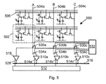
- a pixel array 500 has a matrix of pixels 502. Each column of pixels 502 in the pixel array 500 is connected by a common column bitline 504a, 504b, 504c. Each row of pixels 502 is connected by a common row select 506. The values of the pixels 502 are read out in parallel on to the column bitline 504a, 504b, 504c.
- a horizontal scan 512 sends an "enable signal" along a series of enable connections 514a, 514b, 514c to readout amplifiers 510a, 510b, 510c in turn. The amplified pixel value can then be read on an output bus 516.
- An additional readout amplifier 518 is connected to the bitlines 504a, 504b, 504c by first switch means, which in this example are first FETs 530a, 530b, 530c.
- a second switch means which in this example are second FETs 534a, 534b, 534c, connects the readout amplifiers 510a, 510b, 510c and the column bitlines 504a, 504b, 504c.
- a configuration storage means 532 is connected to each gate of the first and second FETs enabling control of the connection between drain and source. If a defective readout amplifier is detected, then the readout amplifier can be isolated from the bitline avoiding loading the pixel with both the defective amplifier and the additional readout amplifier.
- the configuration storage means 532 may be increased in size, from that of the configuration storage means 432, to accommodate the extra storage required to accommodate the first and second FETs.
- the second FET is switched "off", to disconnect the readout amplifier with the bitline.
- first FET 530a is siwtched "on” and second FET 534a is switched off.
- each second FET 534a, 534b, 534c will typically be switched as opposite to each first FET 530a, 530b, 504c.
- the configuration storage means 532 only requires to store the configuration of one set of FETs.
- a simple inverter can then be used to connect the configuration storage means 532 with the other set of FETs.
- the configuration storage means 532 is connected to the gate of first FET 530a and stores that the first FET 530a should be "off", or open, as the readout amplifier 510a is not defective.
- the gate of second FET 534a can then be connected to an inverter (not shown), which is then connected to the connection between the gate of the first FET 530a and the configuration storage means 532.
Landscapes
- Engineering & Computer Science (AREA)
- Multimedia (AREA)
- Signal Processing (AREA)
- Transforming Light Signals Into Electric Signals (AREA)
- Solid State Image Pick-Up Elements (AREA)
Abstract
Description
- The present invention relates to an image sensor and particularly to an image sensor with readout amplifier redundancy.
- There is an increasing tendency for larger number of pixels on image sensors used in devices such as digital still cameras, mobile phone cameras and mice sensors, for example. Consequently, sensors have either increased in size or pixels have been manufactured smaller, or often both. The use of finer geometry technologies increase the chance of defects occurring. Typically, the defectivity of an image sensor is proportional to the area.
- Defects are caused during manufacture and are usually caused by dust particles obstructing the photolithography process. Resulting defects may be open circuit or short circuit connections.
- If a defect occurs within a pixel during manufacture, a defective pixel is usually the result. The defective pixel can be either ignored by the user or, if the defective pixel can be identified, corrected for by interpolating between neighbouring pixels.
- If the defect occurs on a connection that is common to either a row or column of the pixel array, then a series of pixels in the row or column may be defective, rather than a single pixel. In some cases, the entire row or column can be defective. Defects that disrupt the operation of more than one pixel are far more noticeable to a user and much harder to compensate for.
- Typically, as shown in Fig. 1, a
pixel array 100 has a matrix ofpixels 102. Each column ofpixels 102 in thepixel array 100 is connected by a common column bitline 104. Each row ofpixels 102 is connected by acommon row select 106. When the row select 106 is activated (set to "high") byrow drivers 108, the pixels 110 in that row are enabled for readout and the values of thepixels 102 are read out in parallel on to the column bitline 104 to readoutamplifiers - A
horizontal scan 112 sends an "enable signal" along enable connection 114 to each readout amplifier 110 in turn. The amplified pixel value can then be read on anoutput bus 116. - If the readout amplifier 110 is defective, the entire column of pixels cannot be readout correctly and, as such, a noticeable error occurs in the image.
-
US 6,741,754 Hamilton, "Correcting for defects in a digital image taken by an image sensor caused by pre-existing defects in two pixels in adjacent columns of an image sensor", discloses a method for correcting for defects in a digital image taken by an image sensor when there.are pre-existing defects in two pixels in adjacent columns of the image sensor which causes two adjacent lines of pixels in the digital image to have corrupted data. -
US 5,436,659 , "Method and apparatus for determining defective pixel location", attempts to use digital timing techniques to identify defective pixels and store their locations for correction by an appropriate technique, such as substituting a neighbouring pixel value. -
US 5,291,293 , "Electronic imaging device with defect correction", utilizes redundant sensor elements for defect compensation by using a plurality of arrays and pixels in one sensor used to correct info on the other sensor. - According to the present invention there is provided an image sensor having a plurality of pixels arranged in rows and columns to form a pixel array, each pixel column having a column bitline, the image sensor comprising a column readout for each column bitline and at least one additional column readout, wherein the at least one additional column readout may be selectively connected to one of the column bitlines.
- Preferably, the at least one additional column readout may be selectively connected to one or more column bitlines by a first switch means.
- Preferably, each column readout may be selectively disconnected from the respective column bitline by a second switch means.
- Switch means, in this context, includes one-time on or off switches, such as fuses, as well as other types of switches which may be alternated between on and off.
- In one embodiment, the first switch means and the second switch means are fuse links.
- In an alternative embodiment, the image sensor further comprises a configuration storage means and the first switch means is a first electronic device operable by the configuration storage means.
- Preferably, the second switch means is a second electronic device operable by the configuration storage means.
- Preferably, the configuration storage means is connected by a first connection to one of the first or second electronic devices and the other of the first or second electronic devices is connected to an inverter which is also connected to the first connection.
- Preferably the first and second electronic devices are transistors and further preferably the transistors are PMOS, NMOS or CMOS Field Effect Transistors (FETs).
- CMOS FETs are defined as a combination of PMOS and NMOS transistors.
- According to a second aspect of the present invention there is provided an optical pointing device comprising an image sensor according to the first aspect of the invention.
- Preferably, the optical pointing device is an optical mouse.
- According to a third aspect of the present invention there is provided a mobile device comprising an image sensor according to the first aspect of the invention.
- Preferably, the mobile device is one or more of the following: a mobile cellular telephone; a camera; a portable computer; a Palm device; or a Web Cam.
- According to a fourth aspect of the present invention there is provided a X-ray detection device comprising an image sensor according to the first aspect of the invention.
- Embodiments of the present invention will now be described, by way of example only, with reference to the accompanying drawings, in which;
- Fig. 1 illustrates a prior art image sensor having an array of pixels and readout circuitry;
- Fig. 2 illustrates an image sensor, according to one embodiment of the present invention, having an array of pixels, an additional readout device and a first configuration of fusable links.
- Fig. 3 illustrates an image sensor, according to another embodiment of the present invention, having an array of pixels, an additional readout device and a second configuration of fusable links.
- Fig. 4 illustrates an image sensor, according to another embodiment of the present invention, having an array of pixels, an additional readout device, a readout selection means and a first configuration of transistor switching means; and
- Fig. 5 illustrates an image sensor, according to another embodiment of the present invention, having an array of pixels, an additional readout device, a readout selection means and a second configuration of transistor switching means.
- Typically, two types of issues cause pixel column faults: problems connecting pixels in the readout ("bitline"); and defective column readout.
- "Column readout" is used as a generic term to describe pixel readout circuitry, which is usually on a per column basis. The column readout may be a simple voltage or charge amplifier; with modern technology, it usually incorporates an analogue-digital converter (ADC). The column readout usually also has other processing, such as CDS (correlated double sampling) or other fixed-pattern noise or offset reduction methods. In the context of this invention, "column readout" includes any circuitry connected to a column bitline for reading pixel values.
- With prior-art sensors, if there is a defective column readout circuit, either the whole sensor is declared defective, or the system forced to use some digital correction, which is never 100% transparent and requires post-processing. Post-processing requires additional circuitry, which ultimately increases cost and power usage.
- With "low end" digital cameras, the cost of the image sensor is at a premium and so the sensor is designed to be a small as possible. The size of a pixel is often limited by the size of the column circuitry, so in this case there is no possibility to make the column narrower. Typically, the width of the column circuitry is in the region of 2pm - 5µm.
- In devices such as those found in the "prosumer" market, including digital SLR (single lens reflex) cameras and also professional cameras, the image sensors are large (for example 1/3 or 1/2 or 2/3 the 35mm format or larger). Pixels are also large to enable them to have a "large full well" and store a large number of electrons, thereby reducing photon shot noise. Photon shot noise is the most significant source of noise when the sensor is used on an illuminated scene. As dictated by quantum mechanics, the photons on the sensor follow a Poisson distribution. The Poisson distribution gives the variation in number (i.e. the noise in the signal) proportional to the square-root of the mean. Hence, the pixel's signal to noise ratio, which is the mean divided by the noise, is now proportional to the mean of the number of photons. Therefore, a less noisy pixel has a large capacity to store photons.
- Increasing the full well results in pixels greater than the minimum column readout circuitry, usually a column amplifier, pitch. As these sensors are also large, they are expensive and yield enhancement techniques are especially desirable. Typical pixel width are 5µm-30µm.
- Column readout circuitry, and specifically the readout amplifier, due to its complexity and demanding specification, is unfortunately an area which has a high probability of defectivity.
- The following embodiments are described with reference to readout amplifiers as the column readout circuitry. It should be appreciated that additional, and alternative, readout circuitry components may be present, such as those described previously.
- With prior-art sensors, a defective readout amplifier results in a defective column and hence a large number of defective pixels. Even more problematic, is that the defective pixels are grouped together, which produces a more noticeable error in a final image.
- Referring to Fig. 2, in an embodiment of the invention, a
pixel array 200 has a matrix ofpixels 202. Each column ofpixels 202 in thepixel array 200 is connected by a common column bitline 204. Each row ofpixels 202 is connected by a common row select 206. When the row select 206 is activated (set to "high") by row drivers (not shown), the pixels 210 in that row are enabled for readout and the values of thepixels 202 are read out in parallel on to the column bitline 204 to readout amplifiers 210. - A
horizontal scan 212 sends an "enable signal" along a series of enable connections 214 to each readout amplifier 210 in turn. The amplified pixel value can then be read on anoutput bus 216. - An
additional readout amplifier 218 is connected to the bitlines 204 byfirst fuse links second fuse links horizontal scan 212. Theadditional readout amplifier 218 has an additional enable connection 224 connected to the enable connections 214 bythird fuse links second fuse links horizontal scan 212. - The
additional readout amplifier 218 is a "spare", which can be used if one of the other readout amplifiers 210 is defective. - During a programming phase, typically performed during a manufacturing test phase of the image sensor fabrication, the
image sensor 100 is illuminated and images are acquired. These images are then analyzed to determine if there are defective columns, which may highlight a defective readout amplifier. - If a defective column is located, then it can be bypassed by modifying the first, second and third fuse links. There are various ways of achieving this, one requires making fuse links with machines such as "Focussed Ion Beams", but this tends to be rather slow and expensive. A more common technology is fusable links. These are fabricated as short-circuits during manufacture and can be programmed open by passing a high current which "blows the fuse". Another alternative would be to use short metal or polysilicon traces which are then cut by a high powered laser.
- If, during the test phase, all the columns on the image sensor are found to be operational, then the links are set as shown in Table 1.
Table 1: Link settings where readout amplifiers are not defective LINK OPEN/ SHORT 220a OPEN 220b OPEN 220c OPEN 222a SHORT 222b SHORT 222c SHORT 226a OPEN 226b OPEN 226c OPEN - If, for example, readout amplifier 210b is defective, then the fuse links would be set as in Table 2.
Table 2 : Link settings where column B readout amplifier 210b is defective LINK OPEN/ SHORT 220a OPEN 220b SHORT 220c OPEN 222a SHORT 222b OPEN 222c SHORT 226a OPEN 226b SHORT 226c OPEN - With this pattern of link settings,
column bitline 204b is disconnected from readout amplifier 210b and connected to theadditional readout amplifier 218. - The readout sequence is maintained as the enable
connection 214b is also disconnected from the readout amplifier 210b and connected to theadditional readout amplifier 218. - An alternative embodiment of the invention is shown in Fig 3. Once again, a
pixel array 300 has a matrix ofpixels 302. Each column ofpixels 302 in thepixel array 300 is connected by acommon column bitline pixels 302 is connected by a common row select 306. The values of thepixels 302 are read out in parallel on to thecolumn bitline readout amplifiers horizontal scan 312 sends an "enable signal" along a series of enableconnections readout amplifier output bus 316. Anadditional readout amplifier 318 is connected to the bitlines 304a, 304b, 304c byfirst fuse links - In this embodiment of the invention, there is an additional enable
connection 328 from thehorizontal scan 312. Consequently, eachreadout amplifier - If there are no defects in the
readout amplifiers horizontal scan 312 enables the readout amplifiers in the following order: 310a, 310b then 310c.Fuse links - If there is a defect in
readout amplifier 310b, then thehorizontal scan 312 enables the readout amplifiers in the following order: 310a, 318 then 310c.Fuse links - One method of enabling the
horizontal scan 312 to modify the order in which it enables readout amplifiers is to have a RAM-based look-up table (LUT) incorporated into an address generator. Address generator circuitry is a normal component in an image sensor and therefore would only require slight modification. The address of defective columns would be stored in the RAM. The address generator would increment as normal, but if it reached a value stored in the LUT, then the address of the additional readout amplifier would be used. If the number of columns in the image sensor were a power-of-two, the additional readout amplifier address would have a constant value for the lower number of bits, simplifying the implementation of the counter. - Other methods of enabling the
horizontal scan 312 to modify the order in which it enables readout would be apparent to those skilled in the art. - If the fuse links in the above embodiments are "one-time" fuse links, when testing for defective readout amplifiers, all the fuse links must be kept as short circuit during the sensor test. In the example in Fig. 2 and Fig. 3, keeping the fuse links as short circuit effectively puts three columns in parallel, degrading system performance by reducing the resolution of the system. In any case, the performance of the column amplifiers can still be assessed and the appropriate links blown.
- An alternative embodiment is shown in Figure 4. As before, a
pixel array 400 has a matrix ofpixels 402. Each column ofpixels 402 in thepixel array 400 is connected by acommon column bitline pixels 402 is connected by a common row select 406. The values of thepixels 402 are read out in parallel on to thecolumn bitline readout amplifiers horizontal scan 412 sends an "enable signal" along a series of enableconnections readout amplifier output bus 416. - In this embodiment, an
additional readout amplifier 418 is connected to the bitlines 404a, 404b, 404c by switch means. In this case, the switch means are field effect transistors (FETs) 430a, 430b, 430c operated as switches. - The
FETs additional readout amplifier 418 and enable thereadout amplifiers additional readout amplifier 418. Although theFETs - If a defect is found and the
additional readout amplifier 418 is used, then the input to the defective column amplifier is connected in parallel to theadditional readout amplifier 418. If the readout amplifier has a high input impedance then this is not a problem. However, a readout amplifier's input usually incorporates an active load to facilitate the operation of the pixel's source-follower. In this case, having two inputs in parallel will effectively double the current through the pixel's output, leading to mismatch and other undesirable effects. - An alternative embodiment is shown in Fig. 5. As before, a
pixel array 500 has a matrix ofpixels 502. Each column ofpixels 502 in thepixel array 500 is connected by acommon column bitline pixels 502 is connected by a common row select 506. The values of thepixels 502 are read out in parallel on to thecolumn bitline horizontal scan 512 sends an "enable signal" along a series of enableconnections readout amplifiers output bus 516. - An
additional readout amplifier 518 is connected to the bitlines 504a, 504b, 504c by first switch means, which in this example arefirst FETs - A second switch means, which in this example are
second FETs readout amplifiers - The configuration storage means 532 may be increased in size, from that of the configuration storage means 432, to accommodate the extra storage required to accommodate the first and second FETs. In this configuration, when a first FET is switched "on", to connect a bitline with the
additional readout amplifer 518, the second FET is switched "off", to disconnect the readout amplifier with the bitline. For example, ifreadout amplifier 510a is defective,first FET 530a is siwtched "on" andsecond FET 534a is switched off. Furthermore, it holds true that eachsecond FET first FET - As such, the configuration storage means 532 only requires to store the configuration of one set of FETs. A simple inverter can then be used to connect the configuration storage means 532 with the other set of FETs. For example, the configuration storage means 532 is connected to the gate of
first FET 530a and stores that thefirst FET 530a should be "off", or open, as thereadout amplifier 510a is not defective. The gate ofsecond FET 534a can then be connected to an inverter (not shown), which is then connected to the connection between the gate of thefirst FET 530a and the configuration storage means 532. - In the embodiments described herein, three columns of pixels are shown in each case with one additional readout amplifier providing redundancy if a readout amplifier is defective. It should be appreciated that the invention allows for any combination of number of additional readout amplifiers to columns of pixels. Typically, this is dictated by the available space in the pixel array and relates to the width of the pixel in relation to the width of the readout amplifier. The present invention would also cover the situation where additional readout amplifiers where provided external to the pixel array.
- Improvements and modifications may be incorporated without departing from the scope of the present invention.
Claims (17)
- An image sensor having a plurality of pixels arranged in rows and columns to form a pixel array, each pixel column having a column bitline, the image sensor comprising a column readout for each column bitline and at least one additional column readout, wherein the at least one additional column readout may be selectively connected to one of the column bitlines.
- An image sensor as claimed in claim 1, wherein the at least one additional column readout may be selectively connected to one or more column bitlines by a first switch means.
- An image sensor as claimed in claim 1 or claim 2, wherein each column readout may be selectively disconnected from the respective column bitline by a second switch means.
- An image sensor as claimed in claim 2 or claim 3, further comprising a configuration storage means and the first switch means is a first electronic device operable by the configuration storage means.
- An image sensor as claimed in claim 3 or claim 4, wherein the second switch means is a second electronic device operable by the configuration storage means.
- An image sensor as claimed in claim 5, wherein the configuration storage means is connected by a first connection to one of the first or second electronic devices and the other of the first or second electronic devices is connected to an inverter which is also connected to the first connection.
- An image sensor as claimed in claim 4, wherein the first electronic device is a transistor.
- An image sensor as claimed in claim 5, wherein the second electronic device is a transistor.
- An image sensor as claimed in claim 7 or claim 8, wherein the transistors are PMOS, NMOS or CMOS Field Effect Transistors (FETs).
- An image sensor as claimed in claim 2, wherein the first switch means are one or more fuse links.
- An image sensor as claimed in claim 3, wherein the second switch means are one or more fuse links.
- An image sensor as claimed in any preceding claim, wherein the column readout comprises one or more of the following: a readout amplifier, an analogue-to-digital converter, fixed pattern noise reduction means, offset reduction means.
- An optical pointing device comprising an image sensor according to any of claims 1 to 12.
- An optical pointing device as claimed in claim 13, wherein the optical pointing device is an optical mouse.
- A mobile device comprising an image sensor according to any of claims 1 to 12.
- A mobile device as claimed in claim 15, wherein the mobile device is one or more of the following: a mobile cellular telephone; a camera; a portable computer; a Palm device; or a Web Cam.
- An X-ray detection device comprising an image sensor according to any of claims 1 to 12.
Priority Applications (3)
| Application Number | Priority Date | Filing Date | Title |
|---|---|---|---|
| DE602005016374T DE602005016374D1 (en) | 2005-05-19 | 2005-05-19 | image sensor |
| EP05253114A EP1724837B1 (en) | 2005-05-19 | 2005-05-19 | Image sensor |
| US11/419,044 US7473881B2 (en) | 2005-05-19 | 2006-05-18 | Image sensor |
Applications Claiming Priority (1)
| Application Number | Priority Date | Filing Date | Title |
|---|---|---|---|
| EP05253114A EP1724837B1 (en) | 2005-05-19 | 2005-05-19 | Image sensor |
Publications (2)
| Publication Number | Publication Date |
|---|---|
| EP1724837A1 true EP1724837A1 (en) | 2006-11-22 |
| EP1724837B1 EP1724837B1 (en) | 2009-09-02 |
Family
ID=35106880
Family Applications (1)
| Application Number | Title | Priority Date | Filing Date |
|---|---|---|---|
| EP05253114A Expired - Lifetime EP1724837B1 (en) | 2005-05-19 | 2005-05-19 | Image sensor |
Country Status (3)
| Country | Link |
|---|---|
| US (1) | US7473881B2 (en) |
| EP (1) | EP1724837B1 (en) |
| DE (1) | DE602005016374D1 (en) |
Cited By (2)
| Publication number | Priority date | Publication date | Assignee | Title |
|---|---|---|---|---|
| DE102007058973A1 (en) * | 2007-12-07 | 2009-06-18 | Arnold & Richter Cine Technik Gmbh & Co. Betriebs Kg | image sensor |
| EP1825667A4 (en) * | 2004-12-14 | 2010-07-28 | Bae Systems Information | SUBSTITUTION OF FAULTY READING CIRCUITS OF IMAGING SYSTEMS |
Families Citing this family (10)
| Publication number | Priority date | Publication date | Assignee | Title |
|---|---|---|---|---|
| CN101355659A (en) * | 2007-07-27 | 2009-01-28 | 鸿富锦精密工业(深圳)有限公司 | Solid State Image Sensor |
| TWI349366B (en) * | 2007-10-25 | 2011-09-21 | Novatek Microelectronics Corp | Image sensor and related method with functions of repairing column readout circuits |
| US20100002115A1 (en) * | 2008-07-03 | 2010-01-07 | Xinqiao Liu | Method for Fabricating Large Photo-Diode Arrays |
| US9055249B2 (en) * | 2011-03-28 | 2015-06-09 | Semiconductor Components Industries, Llc | CMOS image sensor with built in correction for column failure |
| US9918029B2 (en) * | 2013-03-14 | 2018-03-13 | Semiconductor Components Industries, Llc | Imaging systems with switchable column power control |
| US9605950B2 (en) * | 2013-05-22 | 2017-03-28 | Cognex Corporation | System and method for efficient surface measurement using a laser displacement sensor |
| DE102014107143B4 (en) * | 2013-05-22 | 2021-03-04 | Cognex Corp. | System and method for measuring the displacement of an object surface |
| JP6184761B2 (en) * | 2013-06-11 | 2017-08-23 | 浜松ホトニクス株式会社 | Solid-state imaging device |
| EP3739872B1 (en) | 2019-05-17 | 2022-02-23 | Teledyne Innovaciones Microelectrónicas, SLU | Cmos optical sensor with a scalable repairing scheme to repair defective readout channels providing a further function of row noise suppression and corresponding row noise suppression method |
| CN111757033A (en) * | 2020-06-30 | 2020-10-09 | 西安微电子技术研究所 | Column readout circuit calibration system and method for CMOS image sensor |
Citations (5)
| Publication number | Priority date | Publication date | Assignee | Title |
|---|---|---|---|---|
| US5291293A (en) | 1992-06-01 | 1994-03-01 | Eastman Kodak Company | Electronic imaging device with defect correction |
| US5436659A (en) | 1991-05-10 | 1995-07-25 | Eastman Kodak Company | Method and apparatus for determining defective pixel location |
| WO1999016238A1 (en) * | 1997-09-22 | 1999-04-01 | Interuniversitair Micro-Elektronica Centrum | Devices and methods for improving the image quality in an image sensor |
| US20020017666A1 (en) * | 2000-06-15 | 2002-02-14 | Takamasa Ishii | Semiconductor device, radiation detection device, and radiation detection system |
| US6741754B2 (en) | 2001-02-19 | 2004-05-25 | Eastman Kodak Company | Correcting for defects in a digital image taken by an image sensor caused by pre-existing defects in two pixels in adjacent columns of an image sensor |
Family Cites Families (4)
| Publication number | Priority date | Publication date | Assignee | Title |
|---|---|---|---|---|
| US6423582B1 (en) * | 1999-02-25 | 2002-07-23 | Micron Technology, Inc. | Use of DAR coating to modulate the efficiency of laser fuse blows |
| US6215113B1 (en) | 1999-04-22 | 2001-04-10 | National Science Council | CMOS active pixel sensor |
| US7385166B2 (en) * | 2003-10-30 | 2008-06-10 | Micron Technology, Inc. | In-pixel kTC noise suppression using circuit techniques |
| US7619669B2 (en) * | 2003-12-29 | 2009-11-17 | Micron Technologies, Inc. | Power savings with multiple readout circuits |
-
2005
- 2005-05-19 EP EP05253114A patent/EP1724837B1/en not_active Expired - Lifetime
- 2005-05-19 DE DE602005016374T patent/DE602005016374D1/en not_active Expired - Lifetime
-
2006
- 2006-05-18 US US11/419,044 patent/US7473881B2/en active Active
Patent Citations (5)
| Publication number | Priority date | Publication date | Assignee | Title |
|---|---|---|---|---|
| US5436659A (en) | 1991-05-10 | 1995-07-25 | Eastman Kodak Company | Method and apparatus for determining defective pixel location |
| US5291293A (en) | 1992-06-01 | 1994-03-01 | Eastman Kodak Company | Electronic imaging device with defect correction |
| WO1999016238A1 (en) * | 1997-09-22 | 1999-04-01 | Interuniversitair Micro-Elektronica Centrum | Devices and methods for improving the image quality in an image sensor |
| US20020017666A1 (en) * | 2000-06-15 | 2002-02-14 | Takamasa Ishii | Semiconductor device, radiation detection device, and radiation detection system |
| US6741754B2 (en) | 2001-02-19 | 2004-05-25 | Eastman Kodak Company | Correcting for defects in a digital image taken by an image sensor caused by pre-existing defects in two pixels in adjacent columns of an image sensor |
Cited By (3)
| Publication number | Priority date | Publication date | Assignee | Title |
|---|---|---|---|---|
| EP1825667A4 (en) * | 2004-12-14 | 2010-07-28 | Bae Systems Information | SUBSTITUTION OF FAULTY READING CIRCUITS OF IMAGING SYSTEMS |
| DE102007058973A1 (en) * | 2007-12-07 | 2009-06-18 | Arnold & Richter Cine Technik Gmbh & Co. Betriebs Kg | image sensor |
| US8154637B2 (en) | 2007-12-07 | 2012-04-10 | Arnold & Richter Cine Technik Gmbh & Co. Betriebs Kg | Image sensor |
Also Published As
| Publication number | Publication date |
|---|---|
| EP1724837B1 (en) | 2009-09-02 |
| DE602005016374D1 (en) | 2009-10-15 |
| US20060261255A1 (en) | 2006-11-23 |
| US7473881B2 (en) | 2009-01-06 |
Similar Documents
| Publication | Publication Date | Title |
|---|---|---|
| EP1724837B1 (en) | Image sensor | |
| US8400546B2 (en) | Image capturing device, image capturing system, and method of driving image capturing device | |
| JP4247514B2 (en) | Method and system for correcting defective pixels | |
| CN100393109C (en) | Signal processing device and method | |
| US7872645B2 (en) | On-chip test system and method for active pixel sensor arrays | |
| JP4931238B2 (en) | Imaging apparatus and driving method thereof | |
| US20120001057A1 (en) | Solid-state imaging apparatus and imaging apparatus | |
| JP2008199254A (en) | Solid-state imaging device, driving method thereof, and imaging device | |
| JP2005217771A (en) | Imaging device | |
| US20090278963A1 (en) | Apparatus and method for column fixed pattern noise (FPN) correction | |
| EP3598740A1 (en) | Image sensor and output compensation circuit of image sensor | |
| US20040012697A1 (en) | Varying capacitance that receives signals from sensing elements | |
| US7443436B2 (en) | Image pickup system for preventing image darkening due to the entrance of intense light | |
| US20190379852A1 (en) | Imaging device and camera | |
| US20090295966A1 (en) | Solid-state imaging device and camera | |
| US20170054926A1 (en) | Imaging apparatus and imaging system | |
| KR100874935B1 (en) | White point defect correction circuit and image sensor using this white point defect correction circuit | |
| CN117529932A (en) | Solid-state imaging device and imaging device | |
| JP4018644B2 (en) | Photoelectric conversion device and imaging system using the same | |
| EP0940031A1 (en) | Devices and methods for improving the image quality in an image sensor | |
| US20070076101A1 (en) | Self-calibrating and/or self-testing camera module | |
| CN106375686A (en) | Method and apparatus for reducing fixed pattern noise in an image sensor in the digital domain | |
| US10484636B2 (en) | Redundancy in active pixel sensors | |
| US20100092027A1 (en) | Image sensor and method | |
| US20030226984A1 (en) | Method of and apparatus for reading out image and method of and apparatus for outputting correction information |
Legal Events
| Date | Code | Title | Description |
|---|---|---|---|
| PUAI | Public reference made under article 153(3) epc to a published international application that has entered the european phase |
Free format text: ORIGINAL CODE: 0009012 |
|
| AK | Designated contracting states |
Kind code of ref document: A1 Designated state(s): AT BE BG CH CY CZ DE DK EE ES FI FR GB GR HU IE IS IT LI LT LU MC NL PL PT RO SE SI SK TR |
|
| AX | Request for extension of the european patent |
Extension state: AL BA HR LV MK YU |
|
| 17P | Request for examination filed |
Effective date: 20070510 |
|
| 17Q | First examination report despatched |
Effective date: 20070608 |
|
| AKX | Designation fees paid |
Designated state(s): DE FR GB IT |
|
| GRAP | Despatch of communication of intention to grant a patent |
Free format text: ORIGINAL CODE: EPIDOSNIGR1 |
|
| GRAS | Grant fee paid |
Free format text: ORIGINAL CODE: EPIDOSNIGR3 |
|
| GRAA | (expected) grant |
Free format text: ORIGINAL CODE: 0009210 |
|
| AK | Designated contracting states |
Kind code of ref document: B1 Designated state(s): DE FR GB IT |
|
| REF | Corresponds to: |
Ref document number: 602005016374 Country of ref document: DE Date of ref document: 20091015 Kind code of ref document: P |
|
| PLBE | No opposition filed within time limit |
Free format text: ORIGINAL CODE: 0009261 |
|
| STAA | Information on the status of an ep patent application or granted ep patent |
Free format text: STATUS: NO OPPOSITION FILED WITHIN TIME LIMIT |
|
| 26N | No opposition filed |
Effective date: 20100603 |
|
| PG25 | Lapsed in a contracting state [announced via postgrant information from national office to epo] |
Ref country code: IT Free format text: LAPSE BECAUSE OF FAILURE TO SUBMIT A TRANSLATION OF THE DESCRIPTION OR TO PAY THE FEE WITHIN THE PRESCRIBED TIME-LIMIT Effective date: 20090902 |
|
| REG | Reference to a national code |
Ref country code: FR Ref legal event code: PLFP Year of fee payment: 12 |
|
| REG | Reference to a national code |
Ref country code: FR Ref legal event code: PLFP Year of fee payment: 13 |
|
| REG | Reference to a national code |
Ref country code: FR Ref legal event code: PLFP Year of fee payment: 14 |
|
| PGFP | Annual fee paid to national office [announced via postgrant information from national office to epo] |
Ref country code: GB Payment date: 20240419 Year of fee payment: 20 |
|
| PGFP | Annual fee paid to national office [announced via postgrant information from national office to epo] |
Ref country code: DE Payment date: 20240418 Year of fee payment: 20 |
|
| PGFP | Annual fee paid to national office [announced via postgrant information from national office to epo] |
Ref country code: FR Payment date: 20240418 Year of fee payment: 20 |
|
| REG | Reference to a national code |
Ref country code: DE Ref legal event code: R079 Ref document number: 602005016374 Country of ref document: DE Free format text: PREVIOUS MAIN CLASS: H01L0027146000 Ipc: H10F0039180000 |
|
| REG | Reference to a national code |
Ref country code: DE Ref legal event code: R071 Ref document number: 602005016374 Country of ref document: DE |
|
| REG | Reference to a national code |
Ref country code: GB Ref legal event code: PE20 Expiry date: 20250518 |
|
| PG25 | Lapsed in a contracting state [announced via postgrant information from national office to epo] |
Ref country code: GB Free format text: LAPSE BECAUSE OF EXPIRATION OF PROTECTION Effective date: 20250518 |