EP1722617A1 - Electronic device - Google Patents
Electronic device Download PDFInfo
- Publication number
- EP1722617A1 EP1722617A1 EP05010296A EP05010296A EP1722617A1 EP 1722617 A1 EP1722617 A1 EP 1722617A1 EP 05010296 A EP05010296 A EP 05010296A EP 05010296 A EP05010296 A EP 05010296A EP 1722617 A1 EP1722617 A1 EP 1722617A1
- Authority
- EP
- European Patent Office
- Prior art keywords
- circuit board
- main circuit
- connector
- electronic device
- contact surfaces
- Prior art date
- Legal status (The legal status is an assumption and is not a legal conclusion. Google has not performed a legal analysis and makes no representation as to the accuracy of the status listed.)
- Granted
Links
- 230000013011 mating Effects 0.000 claims abstract description 21
- 238000000034 method Methods 0.000 claims description 4
- 238000004519 manufacturing process Methods 0.000 description 2
- 239000002390 adhesive tape Substances 0.000 description 1
- 230000000295 complement effect Effects 0.000 description 1
- 230000001419 dependent effect Effects 0.000 description 1
Images




Classifications
-
- H—ELECTRICITY
- H05—ELECTRIC TECHNIQUES NOT OTHERWISE PROVIDED FOR
- H05K—PRINTED CIRCUITS; CASINGS OR CONSTRUCTIONAL DETAILS OF ELECTRIC APPARATUS; MANUFACTURE OF ASSEMBLAGES OF ELECTRICAL COMPONENTS
- H05K1/00—Printed circuits
- H05K1/02—Details
- H05K1/11—Printed elements for providing electric connections to or between printed circuits
- H05K1/117—Pads along the edge of rigid circuit boards, e.g. for pluggable connectors
-
- H—ELECTRICITY
- H05—ELECTRIC TECHNIQUES NOT OTHERWISE PROVIDED FOR
- H05K—PRINTED CIRCUITS; CASINGS OR CONSTRUCTIONAL DETAILS OF ELECTRIC APPARATUS; MANUFACTURE OF ASSEMBLAGES OF ELECTRICAL COMPONENTS
- H05K5/00—Casings, cabinets or drawers for electric apparatus
- H05K5/0026—Casings, cabinets or drawers for electric apparatus provided with connectors and printed circuit boards [PCB], e.g. automotive electronic control units
-
- H—ELECTRICITY
- H05—ELECTRIC TECHNIQUES NOT OTHERWISE PROVIDED FOR
- H05K—PRINTED CIRCUITS; CASINGS OR CONSTRUCTIONAL DETAILS OF ELECTRIC APPARATUS; MANUFACTURE OF ASSEMBLAGES OF ELECTRICAL COMPONENTS
- H05K2201/00—Indexing scheme relating to printed circuits covered by H05K1/00
- H05K2201/09—Shape and layout
- H05K2201/09145—Edge details
-
- H—ELECTRICITY
- H05—ELECTRIC TECHNIQUES NOT OTHERWISE PROVIDED FOR
- H05K—PRINTED CIRCUITS; CASINGS OR CONSTRUCTIONAL DETAILS OF ELECTRIC APPARATUS; MANUFACTURE OF ASSEMBLAGES OF ELECTRICAL COMPONENTS
- H05K2201/00—Indexing scheme relating to printed circuits covered by H05K1/00
- H05K2201/10—Details of components or other objects attached to or integrated in a printed circuit board
- H05K2201/10007—Types of components
- H05K2201/10189—Non-printed connector
-
- H—ELECTRICITY
- H05—ELECTRIC TECHNIQUES NOT OTHERWISE PROVIDED FOR
- H05K—PRINTED CIRCUITS; CASINGS OR CONSTRUCTIONAL DETAILS OF ELECTRIC APPARATUS; MANUFACTURE OF ASSEMBLAGES OF ELECTRICAL COMPONENTS
- H05K2201/00—Indexing scheme relating to printed circuits covered by H05K1/00
- H05K2201/10—Details of components or other objects attached to or integrated in a printed circuit board
- H05K2201/10007—Types of components
- H05K2201/10212—Programmable component
-
- H—ELECTRICITY
- H05—ELECTRIC TECHNIQUES NOT OTHERWISE PROVIDED FOR
- H05K—PRINTED CIRCUITS; CASINGS OR CONSTRUCTIONAL DETAILS OF ELECTRIC APPARATUS; MANUFACTURE OF ASSEMBLAGES OF ELECTRICAL COMPONENTS
- H05K2203/00—Indexing scheme relating to apparatus or processes for manufacturing printed circuits covered by H05K3/00
- H05K2203/16—Inspection; Monitoring; Aligning
- H05K2203/168—Wrong mounting prevention
Definitions
- This invention relates to an electronic device, to an update connector adapter and to a system and a method for programming a control unit.
- the invention relates especially to an electronic device which is built in a passenger compartment of a vehicle.
- electronic devices comprising a main circuit board and a housing in which the main circuit board is fixedly arranged.
- These electronic devices are incorporated into a dashboard of a vehicle and are often part of a multimedia system incorporated into the vehicle.
- These multimedia systems often comprise a navigation module for guiding the user to a predetermined destination location, an audio module for reproducing audio data such as CDs, a radio module and/or a telecommunication module.
- These electronic devices normally comprise one main circuit board having one or two main control units for controlling the functioning of the different modules. During the design of these electronic devices and also at the later stage, it is often necessary to transmit a new software to the electronic device.
- a prior art electronic device is shown.
- the electronic device of the prior art comprises a main circuit board 100 and a first control unit and a second control unit 110, 120.
- These microprocessors 110, 120 control the functioning of the different operating modes of the electronic device.
- two update connectors 130, 140 were provided on the main board 100 for connecting a debug interface or any other programming unit providing new data for the two electronic control units 110, 120.
- the electronic device comprising the main board 100 was incorporated into the dashboard of a vehicle, this meant that the electronic build-in device had to be removed from the dashboard, and the housing around the main board (not shown) had to be opened in order to access the two update connectors 130, 140. This made the update of the electronic device complicated.
- an electronic device comprising a main circuit board and a housing in which the main circuit board is fixedly arranged.
- the main circuit board further comprises contact surfaces located on the main circuit board at an edge thereof, wherein the housing further comprises a recess through which a mating connect is connectable to the contact surfaces of the main circuit board by inserting the mating connector into the housing from the outside.
- the arrangement of the contact surfaces located at an edge of the circuit board relative to the recess helps to facilitate the access to the main circuit board.
- the contact surfaces are arranged next to the recess provided in the housing, so that the contact surfaces are accessible by a mating connector which is inserted into the housing from the outside.
- the main board is accessible from the outside by a mating connector so that the housing has not to be opened for accessing the main board or for accessing any electronic device provided on the main board. Additionally, there is no need any more to provide the update connectors on the main board provided in the prior art as shown in Fig. 1, as the contact surfaces of the update connectors are now provided directly on the surface of the main board. This helps to cut down the costs during the manufacturing of the electronic device, as these update connectors need not to be provided on the main circuit board any more. Additionally, the space needed for the connectors provided on the main circuit board need not to be provided either.
- the electronic device can be accessed more easily through the recess provided in the housing, so that the electronic device needs not to be removed from a support structure (e.g. the dashboard of a passenger compartment of a vehicle) in which the electronic device may be incorporated.
- the main circuit board and the electronic device provided on the main circuit board can be addressed by connecting a mating connector through the recess from the outside of the housing.
- At least one control unit for controlling the operating mode of the electronic device is provided on the main circuit board.
- the control unit further comprises at least one contact area through which the control unit can be programmed.
- the control unit needs to have a possibility to upload data to the control unit. These data may comprise a software update or may comprise any other information needed for the functioning of the control unit.
- the contact area of the control unit is one of the contact surfaces located at the edge of the main circuit board, so that the control unit is programmable by connecting the mating connector to the contact surfaces from the outside of the housing and by transmitting programming data to the control unit.
- the design of the main circuit board and the contact surfaces provided on the main circuit board is such that the contact surfaces located at the edge of the main board can be used for directly accessing said at least one control unit provided on the main board for a software update or even for the case no programming software at all is provided in the control unit.
- the new data can be transmitted to the control unit just by connecting the mating connector from the outside to the contact surfaces.
- the opening of the housing and the removing of the electronic device from the support structure is not necessary any more for connecting a programming unit to the main board.
- the electronic device further comprises an operating module on a front surface of the device for operating the electronic device.
- the recess is provided on the front surface on which the operating module is also provided.
- the main circuit board and the recess are located relative to each other in such a way that the housing is a polarizing element preventing the wrong connection of the mating connector to the contact surfaces of the main circuit board.
- the contact surfaces are arranged relative to the housing in such a way that the mating connector coming from the outside can only be connected to the main board in one orientation. The connecting of the mating connector in other orientations is prevented and blocked by the housing of the electronic device.
- the contact surfaces located at the edge of the main board are directly located on a main surface of the main circuit board.
- a support structure such as a connector housing, need not to be provided on the main board.
- the contact surfaces are provided on both sides of the main circuit board, i.e. on the upper and the lower side of the circuit board. This helps to provide as many contact surfaces as possible on a predetermined small amount of space of the main circuit board. These contact surfaces can be used for accessing any modules provided on the main circuit board.
- the main circuit board is designed in such a way that the conductive tracks leading from the contact surfaces of the edge of the main board connect all the important components of the main board to the contact surfaces, so that these components can be addressed through the contact surfaces at the edge of the main board.
- the invention further relates to an update connector adapter comprising an edge connector for contacting contact surfaces provided at an edge of a main circuit board, the adapter further comprising a support structure on which the edge connector is mounted.
- the adapter further comprises at least another connector mounted to the support structure to which a programming unit is connectable for programming the main circuit board.
- the edge connector is the mating connector mentioned above, which is inserted in the housing of the electronic device through the recess and which contacts the contact surfaces provided at the edge of the main circuit board.
- the adapter may further comprise a second connector mounted to the support structure.
- the update connector adapter comprises the edge connector and two other connectors. Preferably, these two other connectors are used for connecting update or debug units to the update connector adapter.
- the support structure further comprises a latch on which the edge connector is provided.
- the latch is preferably designed in such a way that it fits into the recess of the housing of the electronic device. By inserting the latch into the recess, the edge connector contacts the contact surfaces of the main circuit board.
- the invention further relates to a system for programming or updating a control unit of a main circuit board comprising an electronic device as mentioned above and comprising further an update connector adapter as mentioned above, the edge connector being connected to the contact surfaces provided at the edge of the main circuit board.
- the control unit or microprocessor provided on the main board of the electronic device can be updated in a cost-effective way.
- the electronic device can be updated in the mounted state.
- the housing needs not to be opened to access the control unit.
- update connectors need not to be provided on the main circuit board itself.
- a programming unit may be connected to at least one of the connectors of the update connector adapter, the programming data being transmitted from the programming unit through one of the connectors of the update connector module to the edge connector of the update connector adapter and finally to the control unit.
- the invention further relates to a method for programming a control unit of an electronic device comprising the steps of connecting the programming unit to a first connector of an update connector adapter, inserting the update connector adapter into a recess of a housing of the electronic device, connecting an edge connector provided on the update connector adapter to contact surfaces provided at an edge of a main circuit board of the electronic device, the contact surfaces facing the recess.
- the programming data are transmitted from the programming unit via the update connector adapter to the control unit.
- Fig. 1 shows a main circuit board of an electronic device (not shown) of the prior art.
- the update connectors 130 and 140 are provided on the main circuit board 100 for updating the control units 110 and 120.
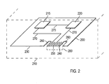
- a main circuit board 200 of an electronic device is shown according to the invention.
- the electronic device comprises a housing 210 which is shown in phantom lines.
- the electronic device may be incorporated into a vehicle or may be incorporated into any other support structure supporting the housing of the electronic device.
- the main circuit board 200 comprises a first control unit 215 connected to the main board 200 and a second control unit 220 connected to the main board 200. It should be understood that the main board 200 can comprise many other electronic components, but they were omitted for the sake of clarity.
- the main circuit board 200 comprises at one of its edges 230 a cantilevered portion or blade 240 on which contact surfaces 250 are provided. At its front end, the blade 240 is separated from the rest of the main board 200 by two cut-outs 260 which receive a mating connector, as will be explained in detail later on.
- circuit board tracks 270 are provided which connect the contact surfaces 250 to the control units 215 and 220.
- a recess 280 is provided in the housing 210 of the electronic device, so that a mating connector (as shown in Fig. 4) may be introduced into the housing for contacting the contact surfaces 250.
- the contact surfaces 250 are provided on the main board and are connected to the control units 115 and 120 in such a way that programming data such as a new software for the control units 110, 120 can be uploaded. Additionally, a debugging unit may be connected to the two control units 110, 120 via the contact surfaces 250 to find a protocol of a faulty operation of the electronic device.
- the two update connectors 130, 140 need not to be provided on the main board 200 any more, this leaving more free space for other electronic components, this also contributing to a cost-effective manufacturing of the electronic device, as the two connectors can be omitted.
- the main circuit board 200 is shown, the housing of the electronic device being omitted for the sake of clarity.
- the main circuit board is shown together with a frame 310 which is provided in the electronic device which helps to support the different electronic modules provided in the electronic device relative to each other.
- the electronic device may be a head unit of a vehicle, comprising different electronic modules such as a navigation module, an audio module, a telecommunication module and/or a radio module. All of these modules are controlled by the main circuit board 200.
- the frame 310 comprises above the contact surfaces 250 a cutout section 320 in order to facilitate the inserting of a mating connector.
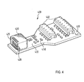
- the adapter 400 comprises a support structure on which an edge connector 420 is provided on a latch 430 of the support structure 410.
- the edge connector 420 is a connector socket having a large opening 425 for receiving the cantilevered part 240 of the main circuit board 200.
- contact terminals 428 are provided in the edge connector contacting the contact surfaces 250.
- the contact terminals 428 may be provided on the upper and the lower part of the housing of the edge connector 420, so that contact surfaces 250 provided on both surfaces of the main circuit board can be contacted.
- update connectors 440 may correspond to the update connectors 130, 140 provided directly on the main circuit board of the prior art. However, any other update connectors may be used. These update connectors can be used for connecting a programming unit such as a user debug interface or any device for uploading data to the control units 215, 220. Connectors such as the two connectors 440 are known in the art, so that a detailed description of the connectors is omitted. Additionally, on the support structure 410, resistors 450 may be provided for adapting the voltage from a programming unit to the voltage supplied to the control unit on the main circuit board 200.
- the update connector adaptor 400 tracks (not shown) are provided for connecting the contact terminals of the two update connectors 440 to the contact terminals of the edge connector 420.
- the two update connectors need only to be provided on the update connector adapter, but they need not to be provided on the main circuit board itself.
- the update connector adapter 400 is shown in its connected state, when it is connected to the contact surfaces 250 of the main circuit board 200.
- the update connector adapter 400 is in a position with the support structure 410 on the upper side, the two update connectors 440 being on the lower side.
- a complementary connector 510 is shown connected to one of the update connectors 440 and the edge connector 420 is slided onto the cantilevered part 240 of the main circuit board 200, the contact elements 428 of the edge connector 420 contacting the contact surfaces 250 provided either on one of the surfaces or on both of the surfaces of the main circuit board 200.
- programming data can be transmitted from a programming unit (not shown) via the ribbon cable 520 through one of the update connectors 440, through the edge connector 420 and the contact surfaces 250 to the control units 215, 220.
- a tuner circuit board 530 is connected to the frame 310 indicating that the electronic device may comprise different electronic modules.
- the housing 210 of the electronic device is shown in a perspective view.
- the electronic device may be incorporated into a support structure such as a dashboard of a vehicle using mounting pegs 610, which are arranged at the side surfaces of the housing.
- an operating module 620 may be provided comprising different operating buttons 630 which can be used for the different operating modes of the electronic device.
- the front surface 650 faces the passenger compartment of the vehicle, when the housing is incorporated into a support structure.
- the recess 280 is also provided on the front surface 650 of the housing, allowing an easy access of the update connector adapter 400, shown in Figs. 4 and 5, even in the mounted state of the housing.
- control units of the device can be configured or updated in an easy way
- a programming unit can be connected to one of the connectors of the update connector adapter
- the update connector adapter can be inserted into the recess 280 of the housing
- the edge connector provided on the update connector adapter can be connected to the contact surfaces provided on the main circuit board.
- the recess 280 is shown covered by a plate 640. If the recess is not used, the opening of the recess 280 should be covered for shielding the electronic device. If programming data need to be transmitted to the control unit, the plate may be removed or bend in such a way that the edge connector 230 can be inserted through the recess 280. When the update connector adapter is removed, the plate 640 should again cover the recess. It is also possible to use an adhesive tape having shielding properties to protect the recess when the latter is not is use.
- the invention provides a possibility for programming a control unit provided in an electronic device in an easy way. Even if the electronic device does not work at all, by way of example, if no software at all is provided in the electronic device for running the latter, this software can be transmitted to the contact surfaces through the recess provided in the housing. Additionally, the main circuit board of the electronic device need not to provide space for accommodating the update connectors, which are moved to the outside and which are provided on the update connector adapter.
Landscapes
- Engineering & Computer Science (AREA)
- Microelectronics & Electronic Packaging (AREA)
- Coupling Device And Connection With Printed Circuit (AREA)
- Combinations Of Printed Boards (AREA)
- Casings For Electric Apparatus (AREA)
Abstract
Description
- This invention relates to an electronic device, to an update connector adapter and to a system and a method for programming a control unit. The invention relates especially to an electronic device which is built in a passenger compartment of a vehicle.
- In the art, electronic devices are known comprising a main circuit board and a housing in which the main circuit board is fixedly arranged. These electronic devices are incorporated into a dashboard of a vehicle and are often part of a multimedia system incorporated into the vehicle. These multimedia systems often comprise a navigation module for guiding the user to a predetermined destination location, an audio module for reproducing audio data such as CDs, a radio module and/or a telecommunication module. These electronic devices normally comprise one main circuit board having one or two main control units for controlling the functioning of the different modules. During the design of these electronic devices and also at the later stage, it is often necessary to transmit a new software to the electronic device.
- In Fig. 1 a prior art electronic device is shown. The electronic device of the prior art comprises a
main circuit board 100 and a first control unit and asecond control unit microprocessors update connectors main board 100 for connecting a debug interface or any other programming unit providing new data for the twoelectronic control units main board 100 was incorporated into the dashboard of a vehicle, this meant that the electronic build-in device had to be removed from the dashboard, and the housing around the main board (not shown) had to be opened in order to access the twoupdate connectors - As a consequence, there is a need to provide a possibility to easily access a main circuit board of an electronic device.
- This need is met by a system and a method as mentioned in the independent claims. In the dependent claims, preferred embodiments of the invention are described.
- According to a first aspect of the invention, an electronic device is provided comprising a main circuit board and a housing in which the main circuit board is fixedly arranged. The main circuit board further comprises contact surfaces located on the main circuit board at an edge thereof, wherein the housing further comprises a recess through which a mating connect is connectable to the contact surfaces of the main circuit board by inserting the mating connector into the housing from the outside. The arrangement of the contact surfaces located at an edge of the circuit board relative to the recess helps to facilitate the access to the main circuit board. The contact surfaces are arranged next to the recess provided in the housing, so that the contact surfaces are accessible by a mating connector which is inserted into the housing from the outside. This arrangement of the contact surfaces located on the main board together with the recess in the housing has several advantages: First of all, the main board is accessible from the outside by a mating connector so that the housing has not to be opened for accessing the main board or for accessing any electronic device provided on the main board. Additionally, there is no need any more to provide the update connectors on the main board provided in the prior art as shown in Fig. 1, as the contact surfaces of the update connectors are now provided directly on the surface of the main board. This helps to cut down the costs during the manufacturing of the electronic device, as these update connectors need not to be provided on the main circuit board any more. Additionally, the space needed for the connectors provided on the main circuit board need not to be provided either. The electronic device can be accessed more easily through the recess provided in the housing, so that the electronic device needs not to be removed from a support structure (e.g. the dashboard of a passenger compartment of a vehicle) in which the electronic device may be incorporated. The main circuit board and the electronic device provided on the main circuit board can be addressed by connecting a mating connector through the recess from the outside of the housing.
- Preferably, at least one control unit for controlling the operating mode of the electronic device is provided on the main circuit board. The control unit further comprises at least one contact area through which the control unit can be programmed. The control unit needs to have a possibility to upload data to the control unit. These data may comprise a software update or may comprise any other information needed for the functioning of the control unit. According to the invention, the contact area of the control unit is one of the contact surfaces located at the edge of the main circuit board, so that the control unit is programmable by connecting the mating connector to the contact surfaces from the outside of the housing and by transmitting programming data to the control unit. The design of the main circuit board and the contact surfaces provided on the main circuit board is such that the contact surfaces located at the edge of the main board can be used for directly accessing said at least one control unit provided on the main board for a software update or even for the case no programming software at all is provided in the control unit. The new data can be transmitted to the control unit just by connecting the mating connector from the outside to the contact surfaces. The opening of the housing and the removing of the electronic device from the support structure is not necessary any more for connecting a programming unit to the main board.
- Preferably, the electronic device further comprises an operating module on a front surface of the device for operating the electronic device. Preferably, the recess is provided on the front surface on which the operating module is also provided. By providing the recess on the same surface as the operating module, it can be assured that the recess can be accessed in all cases, as the operating module for operating the electronic device is normally always accessible to the user of the electronic device. If the operating module is accessible, the recess is also accessible, so that through the recess a meting connector can contact the contact surfaces located at the edge of the main board. The rest of the surfaces of the housing of the electronic device could be hidden by the support structure in which the housing may be arranged.
- Preferably, the main circuit board and the recess are located relative to each other in such a way that the housing is a polarizing element preventing the wrong connection of the mating connector to the contact surfaces of the main circuit board. In this embodiment, the contact surfaces are arranged relative to the housing in such a way that the mating connector coming from the outside can only be connected to the main board in one orientation. The connecting of the mating connector in other orientations is prevented and blocked by the housing of the electronic device.
- According to one embodiment of the invention, the contact surfaces located at the edge of the main board are directly located on a main surface of the main circuit board. By providing the contact surfaces directly on the main surface, a support structure, such as a connector housing, need not to be provided on the main board.
- According to another embodiment of the invention, the contact surfaces are provided on both sides of the main circuit board, i.e. on the upper and the lower side of the circuit board. This helps to provide as many contact surfaces as possible on a predetermined small amount of space of the main circuit board. These contact surfaces can be used for accessing any modules provided on the main circuit board. Preferably, the main circuit board is designed in such a way that the conductive tracks leading from the contact surfaces of the edge of the main board connect all the important components of the main board to the contact surfaces, so that these components can be addressed through the contact surfaces at the edge of the main board.
- The invention further relates to an update connector adapter comprising an edge connector for contacting contact surfaces provided at an edge of a main circuit board, the adapter further comprising a support structure on which the edge connector is mounted. The adapter further comprises at least another connector mounted to the support structure to which a programming unit is connectable for programming the main circuit board. Preferably, the edge connector is the mating connector mentioned above, which is inserted in the housing of the electronic device through the recess and which contacts the contact surfaces provided at the edge of the main circuit board.
- The adapter may further comprise a second connector mounted to the support structure. In this case, the update connector adapter comprises the edge connector and two other connectors. Preferably, these two other connectors are used for connecting update or debug units to the update connector adapter.
- Preferably, the support structure further comprises a latch on which the edge connector is provided. The latch is preferably designed in such a way that it fits into the recess of the housing of the electronic device. By inserting the latch into the recess, the edge connector contacts the contact surfaces of the main circuit board.
- The invention further relates to a system for programming or updating a control unit of a main circuit board comprising an electronic device as mentioned above and comprising further an update connector adapter as mentioned above, the edge connector being connected to the contact surfaces provided at the edge of the main circuit board. Using this system, the control unit or microprocessor provided on the main board of the electronic device can be updated in a cost-effective way. As new data can be transmitted to the control unit without the need of removing the electronic device from a support structure such as a dashboard, the electronic device can be updated in the mounted state. Furthermore, the housing needs not to be opened to access the control unit. Additionally, update connectors need not to be provided on the main circuit board itself. For programming the control unit of the main circuit board, a programming unit may be connected to at least one of the connectors of the update connector adapter, the programming data being transmitted from the programming unit through one of the connectors of the update connector module to the edge connector of the update connector adapter and finally to the control unit.
- The invention further relates to a method for programming a control unit of an electronic device comprising the steps of connecting the programming unit to a first connector of an update connector adapter, inserting the update connector adapter into a recess of a housing of the electronic device, connecting an edge connector provided on the update connector adapter to contact surfaces provided at an edge of a main circuit board of the electronic device, the contact surfaces facing the recess. Last but not least, the programming data are transmitted from the programming unit via the update connector adapter to the control unit.
- Further embodiments of the invention will now be described in more detail with reference to the accompanying drawings, in which
- Fig. 1
- is a schematic view of a main circuit board of the prior art,
- Fig. 2
- is a schematic view of a main circuit board which can be used in an electronic device of the invention,
- Fig. 3
- shows a part of a main circuit board and the contact surfaces provided at an edge thereof,
- Fig. 4
- shows a schematic view of an update connector adapter,
- Fig. 5
- shows the update connector adapter of Fig. 4 in connection to the main circuit board, and
- Fig. 6
- shows a perspective view of an electronic device having a recess for connecting the update connector adapter.
- As already explained in the introductory part of the description, Fig. 1 shows a main circuit board of an electronic device (not shown) of the prior art. In Fig. 1; the
update connectors main circuit board 100 for updating thecontrol units - In Fig. 2, a
main circuit board 200 of an electronic device is shown according to the invention. The electronic device comprises ahousing 210 which is shown in phantom lines. The electronic device may be incorporated into a vehicle or may be incorporated into any other support structure supporting the housing of the electronic device. Themain circuit board 200 comprises afirst control unit 215 connected to themain board 200 and asecond control unit 220 connected to themain board 200. It should be understood that themain board 200 can comprise many other electronic components, but they were omitted for the sake of clarity. - The
main circuit board 200 comprises at one of its edges 230 a cantilevered portion orblade 240 on which contact surfaces 250 are provided. At its front end, theblade 240 is separated from the rest of themain board 200 by two cut-outs 260 which receive a mating connector, as will be explained in detail later on. - On the main board, circuit board tracks 270 are provided which connect the contact surfaces 250 to the
control units housing 210 of the electronic device, arecess 280 is provided at a location facing the contact surfaces 250, so that a mating connector (as shown in Fig. 4) may be introduced into the housing for contacting the contact surfaces 250. - The contact surfaces 250 are provided on the main board and are connected to the
control units 115 and 120 in such a way that programming data such as a new software for thecontrol units control units - When comparing Fig. 1 to Fig. 2, it can be noted that the two
update connectors main board 200 any more, this leaving more free space for other electronic components, this also contributing to a cost-effective manufacturing of the electronic device, as the two connectors can be omitted. - In Fig. 3, part of the
main circuit board 200 is shown, the housing of the electronic device being omitted for the sake of clarity. In the embodiment of Fig. 3, the main circuit board is shown together with aframe 310 which is provided in the electronic device which helps to support the different electronic modules provided in the electronic device relative to each other. The electronic device may be a head unit of a vehicle, comprising different electronic modules such as a navigation module, an audio module, a telecommunication module and/or a radio module. All of these modules are controlled by themain circuit board 200. Theframe 310 comprises above the contact surfaces 250 acutout section 320 in order to facilitate the inserting of a mating connector. - In Fig. 4, an
update connector adapter 400 is shown. Theadapter 400 comprises a support structure on which anedge connector 420 is provided on alatch 430 of thesupport structure 410. Theedge connector 420 is a connector socket having alarge opening 425 for receiving thecantilevered part 240 of themain circuit board 200. Additionally,contact terminals 428 are provided in the edge connector contacting the contact surfaces 250. Thecontact terminals 428 may be provided on the upper and the lower part of the housing of theedge connector 420, so that contact surfaces 250 provided on both surfaces of the main circuit board can be contacted. These edge connectors are known to the person skilled in the art, so that a detailed description of the edge connector can be omitted. - Additionally, on the support structure there are provided two
update connectors 440. These update connectors may correspond to theupdate connectors control units connectors 440 are known in the art, so that a detailed description of the connectors is omitted. Additionally, on thesupport structure 410,resistors 450 may be provided for adapting the voltage from a programming unit to the voltage supplied to the control unit on themain circuit board 200. In theupdate connector adaptor 400 tracks (not shown) are provided for connecting the contact terminals of the twoupdate connectors 440 to the contact terminals of theedge connector 420. As can be seen in Fig. 4, the two update connectors need only to be provided on the update connector adapter, but they need not to be provided on the main circuit board itself. - In Fig. 5, the
update connector adapter 400 is shown in its connected state, when it is connected to the contact surfaces 250 of themain circuit board 200. In the embodiment shown, theupdate connector adapter 400 is in a position with thesupport structure 410 on the upper side, the twoupdate connectors 440 being on the lower side. Additionally, acomplementary connector 510 is shown connected to one of theupdate connectors 440 and theedge connector 420 is slided onto thecantilevered part 240 of themain circuit board 200, thecontact elements 428 of theedge connector 420 contacting the contact surfaces 250 provided either on one of the surfaces or on both of the surfaces of themain circuit board 200. In the connected state shown in Fig. 5, programming data can be transmitted from a programming unit (not shown) via theribbon cable 520 through one of theupdate connectors 440, through theedge connector 420 and the contact surfaces 250 to thecontrol units - In the embodiment shown in Fig. 5, a
tuner circuit board 530 is connected to theframe 310 indicating that the electronic device may comprise different electronic modules. - In Fig. 6, the
housing 210 of the electronic device is shown in a perspective view. The electronic device may be incorporated into a support structure such as a dashboard of a vehicle using mountingpegs 610, which are arranged at the side surfaces of the housing. On the front part of thehousing 210, anoperating module 620 may be provided comprisingdifferent operating buttons 630 which can be used for the different operating modes of the electronic device. Thefront surface 650 faces the passenger compartment of the vehicle, when the housing is incorporated into a support structure. Therecess 280 is also provided on thefront surface 650 of the housing, allowing an easy access of theupdate connector adapter 400, shown in Figs. 4 and 5, even in the mounted state of the housing. - In the mounted state of the housing, the control units of the device can be configured or updated in an easy way, a programming unit can be connected to one of the connectors of the update connector adapter, the update connector adapter can be inserted into the
recess 280 of the housing, and the edge connector provided on the update connector adapter can be connected to the contact surfaces provided on the main circuit board. - In the embodiment shown in Fig. 6, the
recess 280 is shown covered by a plate 640. If the recess is not used, the opening of therecess 280 should be covered for shielding the electronic device. If programming data need to be transmitted to the control unit, the plate may be removed or bend in such a way that theedge connector 230 can be inserted through therecess 280. When the update connector adapter is removed, the plate 640 should again cover the recess. It is also possible to use an adhesive tape having shielding properties to protect the recess when the latter is not is use. - In conclusion, the invention provides a possibility for programming a control unit provided in an electronic device in an easy way. Even if the electronic device does not work at all, by way of example, if no software at all is provided in the electronic device for running the latter, this software can be transmitted to the contact surfaces through the recess provided in the housing. Additionally, the main circuit board of the electronic device need not to provide space for accommodating the update connectors, which are moved to the outside and which are provided on the update connector adapter.
Claims (14)
- Electronic device comprising a main circuit board (200) and a housing (210) in which the main circuit board is fixedly arranged, the main circuit board further comprising contact surfaces (250) located on the main circuit board at an edge thereof, wherein the housing further comprises a recess (280) through which a mating connector (420) is connectable to the contact surfaces (250) of the main circuit board by inserting the mating connector into the housing from the outside.
- Device according to claim 1, characterized in that at least one control unit (215, 220) for controlling the operating mode of the electronic device is provided on said main circuit board (200), the control unit having at least one contact area through which the control unit can be programmed, wherein the contact area is one of the contact surfaces (250) located at the edge of the main circuit board, so that the control unit (215, 220) is programmable by connecting the mating connector (420) to the contact surfaces and by transmitting programming data to the control unit from the outside of the housing.
- Device according to claim 1 or 2, characterized by further comprising an operating module (620) on a front surface (630) of the device for operating the electronic device, wherein the recess (280) is provided on the front surface.
- Device according to any of the preceding claims, characterized in that the main circuit board (200) and the recess (280) are located relative to each other in such a way, that the housing (210) is a polarizing element preventing the wrong connection of the mating connector (420) to the contact surfaces of the main circuit board.
- Device according to any of the preceding claims, characterized in that the contact surfaces (250) are directly located on a main surface of the main circuit board (200).
- Device according to any of the preceding claims, characterized in that the contact surfaces (250) are directly located on opposite surfaces of the main circuit board (200).
- Update connector adapter (400) comprising an edge connector (420) for contacting contact surfaces provided at the edge of a main circuit board, a support structure (410) on which the edge connector is mounted, the adapter further comprising at least another connector (440) mounted to the support structure to which a programming unit is connectable for programming the main circuit board.
- Adapter (400) according to claim 7, characterized by further comprising a second connector (440) mounted to the support structure.
- Adapter (400) according to claim 7 or 8, characterized in that the support structure (410) comprises a latch on which the edge connector (420) is provided.
- Adapter according to any of claims 9, wherein the latch is inserted in the recess of the housing of the electronic device as mentioned in any of claims 1 to 6, the edge connector contacting the contact surfaces of the main circuit board.
- System for programming a control unit of a main circuit board, comprising an electronic device as claimed in any of claims 1 to 6, an update connector adapter (400) as mentioned in any of claims 7 to 10, wherein the edge connector (420) is connected to the contact surfaces (250) at the edge of the main circuit board (200).
- System according to claim 11, characterized in that a programming unit is connected to said at least one connector of the update connector adapter for programming the control unit on the main circuit board.
- Method for programming a control unit of an electronic device comprising the following steps:- connecting a programming unit to a first connector of an update connector adapter,- inserting the update connector adapter (400) into a recess (280) of a housing (210) of the electronic device,- connecting an edge connector (420) provided on the update connector adapter to contact surfaces (250) provided on a main circuit board of the electronic device, the contact surfaces facing the recess, and- transmitting the programming data from the programming unit via the update connector adapter to the control unit.
- Device according to any one of claims 1 to 6, characterized in that the electronic device is a built-in electronic device for a vehicle mountable on a passenger compartment of the vehicle, wherein the recess for introducing the mating connector faces the passenger compartment.
Priority Applications (3)
| Application Number | Priority Date | Filing Date | Title |
|---|---|---|---|
| EP05010296A EP1722617B1 (en) | 2005-05-12 | 2005-05-12 | Electronic device |
| DE602005003455T DE602005003455T2 (en) | 2005-05-12 | 2005-05-12 | Electronic device |
| US11/433,054 US8208263B2 (en) | 2005-05-12 | 2006-05-12 | Electronic device |
Applications Claiming Priority (1)
| Application Number | Priority Date | Filing Date | Title |
|---|---|---|---|
| EP05010296A EP1722617B1 (en) | 2005-05-12 | 2005-05-12 | Electronic device |
Publications (2)
| Publication Number | Publication Date |
|---|---|
| EP1722617A1 true EP1722617A1 (en) | 2006-11-15 |
| EP1722617B1 EP1722617B1 (en) | 2007-11-21 |
Family
ID=35734042
Family Applications (1)
| Application Number | Title | Priority Date | Filing Date |
|---|---|---|---|
| EP05010296A Expired - Lifetime EP1722617B1 (en) | 2005-05-12 | 2005-05-12 | Electronic device |
Country Status (3)
| Country | Link |
|---|---|
| US (1) | US8208263B2 (en) |
| EP (1) | EP1722617B1 (en) |
| DE (1) | DE602005003455T2 (en) |
Cited By (2)
| Publication number | Priority date | Publication date | Assignee | Title |
|---|---|---|---|---|
| ITTO20110059A1 (en) * | 2011-01-25 | 2012-07-26 | Gate Srl | VOLTAGE REGULATOR DEVICE, PARTICULARLY FOR A FANS ASSOCIATED WITH A HEAT EXCHANGER OF A MOTOR VEHICLE |
| EP2927702A1 (en) * | 2014-03-31 | 2015-10-07 | Shinko Electric Industries Co., Ltd. | Semiconductor device with removable wiring board portion for evaluation and corresponding method of manufacturing |
Families Citing this family (1)
| Publication number | Priority date | Publication date | Assignee | Title |
|---|---|---|---|---|
| US9343861B2 (en) * | 2013-01-25 | 2016-05-17 | Tyco Electronics Corporation | Communication module adaptor |
Citations (8)
| Publication number | Priority date | Publication date | Assignee | Title |
|---|---|---|---|---|
| US4152750A (en) * | 1977-04-25 | 1979-05-01 | Allen-Bradley Company | I/O interface rack for solid state control system |
| GB2115989A (en) * | 1982-02-12 | 1983-09-14 | Voltmace Limited | Programmed cartridge/video machine adaptor |
| US4480835A (en) * | 1983-03-02 | 1984-11-06 | Williams Theodore R | Cartridge adapter for programmable video games |
| EP0434192A2 (en) * | 1989-10-24 | 1991-06-26 | International Business Machines Corporation | Offset basecard |
| EP0591657A1 (en) * | 1992-09-30 | 1994-04-13 | International Business Machines Corporation | A common adapter card which is pluggable into computers having different bus architectures |
| EP0654960A1 (en) * | 1993-11-12 | 1995-05-24 | ELCON INSTRUMENTS S.r.l. | A circuit interconnecting device, for use in industrial applications |
| EP0950570A2 (en) * | 1998-03-24 | 1999-10-20 | CLARION Co., Ltd. | Automotive information system, automotive computer system, and method of controlling the automotive information system |
| US20020050384A1 (en) * | 2000-05-18 | 2002-05-02 | Harald Schopp | Multimedia system with a housing that operationally stores a plurality of multimedia modules |
Family Cites Families (16)
| Publication number | Priority date | Publication date | Assignee | Title |
|---|---|---|---|---|
| US5660568A (en) * | 1995-01-04 | 1997-08-26 | Simple Technology, Inc. | Communications card with integral transmission media line adaptor |
| CA2265820A1 (en) * | 1996-09-18 | 1998-03-26 | Craig S. Wood | Gps power/data cable system |
| JPH118025A (en) * | 1997-06-16 | 1999-01-12 | Amp Japan Ltd | Circuit device |
| US6417786B2 (en) * | 1998-11-23 | 2002-07-09 | Lear Automotive Dearborn, Inc. | Vehicle navigation system with removable positioning receiver |
| US6283789B1 (en) * | 2000-03-16 | 2001-09-04 | Shui Chuan Tsai | Data and power transmitting cable system |
| US6909907B1 (en) * | 2000-11-10 | 2005-06-21 | Pharos Science & Applications, Inc. | Integrated connection assembly for global positioning system (GPS) receiver and personal digital assistance (PDA) device or cellular phones |
| JP4963762B2 (en) * | 2001-08-22 | 2012-06-27 | 任天堂株式会社 | Cartridge for game console |
| JP3901501B2 (en) * | 2001-12-12 | 2007-04-04 | アルプス電気株式会社 | Electronic circuit unit mounting structure |
| US6795770B1 (en) * | 2002-04-02 | 2004-09-21 | Garmin Ltd. | Portable navigation device with instant on configuration on navigational display |
| US7440845B1 (en) * | 2003-03-26 | 2008-10-21 | Garmin Ltd. | Navigational device for installation in a vehicle and a method for doing same |
| US6855003B1 (en) * | 2003-10-14 | 2005-02-15 | Brunswick Corporation | Multiple use connector for a GPS system on a marine vessel |
| US7215279B1 (en) * | 2004-06-02 | 2007-05-08 | Garmin Ltd. | Portable navigational device with a remote control, an internal memory, and an internal heating element |
| KR100671302B1 (en) * | 2005-03-08 | 2007-01-19 | 삼성전자주식회사 | Mobile display device |
| US7468692B1 (en) * | 2005-03-15 | 2008-12-23 | Garmin Ltd. | Method and apparatus for interconnecting navigation components using a multi-pin connector |
| US7546634B2 (en) * | 2005-04-08 | 2009-06-09 | Victor Chuan-Chen Wu | Encryption removable storage system |
| US8215991B2 (en) * | 2009-02-26 | 2012-07-10 | Sandisk Il Ltd. | Memory card and host device |
-
2005
- 2005-05-12 DE DE602005003455T patent/DE602005003455T2/en not_active Expired - Lifetime
- 2005-05-12 EP EP05010296A patent/EP1722617B1/en not_active Expired - Lifetime
-
2006
- 2006-05-12 US US11/433,054 patent/US8208263B2/en not_active Expired - Fee Related
Patent Citations (8)
| Publication number | Priority date | Publication date | Assignee | Title |
|---|---|---|---|---|
| US4152750A (en) * | 1977-04-25 | 1979-05-01 | Allen-Bradley Company | I/O interface rack for solid state control system |
| GB2115989A (en) * | 1982-02-12 | 1983-09-14 | Voltmace Limited | Programmed cartridge/video machine adaptor |
| US4480835A (en) * | 1983-03-02 | 1984-11-06 | Williams Theodore R | Cartridge adapter for programmable video games |
| EP0434192A2 (en) * | 1989-10-24 | 1991-06-26 | International Business Machines Corporation | Offset basecard |
| EP0591657A1 (en) * | 1992-09-30 | 1994-04-13 | International Business Machines Corporation | A common adapter card which is pluggable into computers having different bus architectures |
| EP0654960A1 (en) * | 1993-11-12 | 1995-05-24 | ELCON INSTRUMENTS S.r.l. | A circuit interconnecting device, for use in industrial applications |
| EP0950570A2 (en) * | 1998-03-24 | 1999-10-20 | CLARION Co., Ltd. | Automotive information system, automotive computer system, and method of controlling the automotive information system |
| US20020050384A1 (en) * | 2000-05-18 | 2002-05-02 | Harald Schopp | Multimedia system with a housing that operationally stores a plurality of multimedia modules |
Cited By (3)
| Publication number | Priority date | Publication date | Assignee | Title |
|---|---|---|---|---|
| ITTO20110059A1 (en) * | 2011-01-25 | 2012-07-26 | Gate Srl | VOLTAGE REGULATOR DEVICE, PARTICULARLY FOR A FANS ASSOCIATED WITH A HEAT EXCHANGER OF A MOTOR VEHICLE |
| EP2927702A1 (en) * | 2014-03-31 | 2015-10-07 | Shinko Electric Industries Co., Ltd. | Semiconductor device with removable wiring board portion for evaluation and corresponding method of manufacturing |
| US9977074B2 (en) | 2014-03-31 | 2018-05-22 | Shinko Electric Industries Co., Ltd. | Semiconductor device, semiconductor apparatus and method for manufacturing semiconductor device |
Also Published As
| Publication number | Publication date |
|---|---|
| EP1722617B1 (en) | 2007-11-21 |
| US8208263B2 (en) | 2012-06-26 |
| US20070019392A1 (en) | 2007-01-25 |
| DE602005003455D1 (en) | 2008-01-03 |
| DE602005003455T2 (en) | 2008-10-02 |
Similar Documents
| Publication | Publication Date | Title |
|---|---|---|
| EP2054269B1 (en) | Lightweight audio system for automotive applications and method | |
| US6441510B1 (en) | Reconfigurable modular instrument cluster arrangement | |
| US6215656B1 (en) | Method and apparatus for factory or user configurable external connectors | |
| JP4100993B2 (en) | Electronics | |
| US5668698A (en) | Smart connector for an electrical device | |
| US6315582B1 (en) | Electronic device for connecting universal serial buss interface equipment | |
| US20030008554A1 (en) | Connector with mounting fixture for removable storage device | |
| JP5769164B2 (en) | In-vehicle device connection adapter | |
| US7102887B2 (en) | Housing for hot pluggable network taps | |
| EP0434192A2 (en) | Offset basecard | |
| US7453692B2 (en) | Computer device with a modular transmission interface, the modular transmission interface, and an adaptor board | |
| US6511342B1 (en) | Modular instrument panel system having a flat flexible bus | |
| EP1722617B1 (en) | Electronic device | |
| JP3591705B2 (en) | Electronic device erroneous mounting prevention mechanism | |
| CN102265721B (en) | Input/output unit | |
| JP3584466B2 (en) | Disk array | |
| US7085137B2 (en) | Card mounting apparatus | |
| JP5966126B2 (en) | In-vehicle device connection adapter | |
| US20030099100A1 (en) | Adaptive module for housings | |
| JP2004320940A (en) | Electrical connection box for vehicles and circuit block for controlling electrical components | |
| JP6440133B2 (en) | In-vehicle device connection adapter | |
| EP1848258B1 (en) | Computer device with a modular transmission interface, the modular transmission interface, and an adaptor board | |
| JPH11134973A (en) | Combination switch device for multiplex communication | |
| JP2015221663A (en) | Adapter for in-vehicle device connection | |
| JP6452867B2 (en) | In-vehicle device connection adapter |
Legal Events
| Date | Code | Title | Description |
|---|---|---|---|
| PUAI | Public reference made under article 153(3) epc to a published international application that has entered the european phase |
Free format text: ORIGINAL CODE: 0009012 |
|
| AK | Designated contracting states |
Kind code of ref document: A1 Designated state(s): AT BE BG CH CY CZ DE DK EE ES FI FR GB GR HU IE IS IT LI LT LU MC NL PL PT RO SE SI SK TR |
|
| AX | Request for extension of the european patent |
Extension state: AL BA HR LV MK YU |
|
| GRAP | Despatch of communication of intention to grant a patent |
Free format text: ORIGINAL CODE: EPIDOSNIGR1 |
|
| 17P | Request for examination filed |
Effective date: 20070417 |
|
| AKX | Designation fees paid |
Designated state(s): AT BE BG CH CY CZ DE DK EE ES FI FR GB GR HU IE IS IT LI LT LU MC NL PL PT RO SE SI SK TR |
|
| GRAS | Grant fee paid |
Free format text: ORIGINAL CODE: EPIDOSNIGR3 |
|
| GRAA | (expected) grant |
Free format text: ORIGINAL CODE: 0009210 |
|
| AK | Designated contracting states |
Kind code of ref document: B1 Designated state(s): AT BE BG CH CY CZ DE DK EE ES FI FR GB GR HU IE IS IT LI LT LU MC NL PL PT RO SE SI SK TR |
|
| REG | Reference to a national code |
Ref country code: GB Ref legal event code: FG4D |
|
| REG | Reference to a national code |
Ref country code: IE Ref legal event code: FG4D |
|
| REG | Reference to a national code |
Ref country code: CH Ref legal event code: EP |
|
| REF | Corresponds to: |
Ref document number: 602005003455 Country of ref document: DE Date of ref document: 20080103 Kind code of ref document: P |
|
| PG25 | Lapsed in a contracting state [announced via postgrant information from national office to epo] |
Ref country code: NL Free format text: LAPSE BECAUSE OF FAILURE TO SUBMIT A TRANSLATION OF THE DESCRIPTION OR TO PAY THE FEE WITHIN THE PRESCRIBED TIME-LIMIT Effective date: 20071121 Ref country code: LI Free format text: LAPSE BECAUSE OF FAILURE TO SUBMIT A TRANSLATION OF THE DESCRIPTION OR TO PAY THE FEE WITHIN THE PRESCRIBED TIME-LIMIT Effective date: 20071121 Ref country code: ES Free format text: LAPSE BECAUSE OF FAILURE TO SUBMIT A TRANSLATION OF THE DESCRIPTION OR TO PAY THE FEE WITHIN THE PRESCRIBED TIME-LIMIT Effective date: 20080304 Ref country code: CH Free format text: LAPSE BECAUSE OF FAILURE TO SUBMIT A TRANSLATION OF THE DESCRIPTION OR TO PAY THE FEE WITHIN THE PRESCRIBED TIME-LIMIT Effective date: 20071121 Ref country code: SE Free format text: LAPSE BECAUSE OF FAILURE TO SUBMIT A TRANSLATION OF THE DESCRIPTION OR TO PAY THE FEE WITHIN THE PRESCRIBED TIME-LIMIT Effective date: 20080221 |
|
| NLV1 | Nl: lapsed or annulled due to failure to fulfill the requirements of art. 29p and 29m of the patents act | ||
| PG25 | Lapsed in a contracting state [announced via postgrant information from national office to epo] |
Ref country code: BG Free format text: LAPSE BECAUSE OF FAILURE TO SUBMIT A TRANSLATION OF THE DESCRIPTION OR TO PAY THE FEE WITHIN THE PRESCRIBED TIME-LIMIT Effective date: 20080221 Ref country code: IS Free format text: LAPSE BECAUSE OF FAILURE TO SUBMIT A TRANSLATION OF THE DESCRIPTION OR TO PAY THE FEE WITHIN THE PRESCRIBED TIME-LIMIT Effective date: 20080321 Ref country code: LT Free format text: LAPSE BECAUSE OF FAILURE TO SUBMIT A TRANSLATION OF THE DESCRIPTION OR TO PAY THE FEE WITHIN THE PRESCRIBED TIME-LIMIT Effective date: 20071121 Ref country code: SI Free format text: LAPSE BECAUSE OF FAILURE TO SUBMIT A TRANSLATION OF THE DESCRIPTION OR TO PAY THE FEE WITHIN THE PRESCRIBED TIME-LIMIT Effective date: 20071121 Ref country code: FI Free format text: LAPSE BECAUSE OF FAILURE TO SUBMIT A TRANSLATION OF THE DESCRIPTION OR TO PAY THE FEE WITHIN THE PRESCRIBED TIME-LIMIT Effective date: 20071121 Ref country code: PL Free format text: LAPSE BECAUSE OF FAILURE TO SUBMIT A TRANSLATION OF THE DESCRIPTION OR TO PAY THE FEE WITHIN THE PRESCRIBED TIME-LIMIT Effective date: 20071121 |
|
| REG | Reference to a national code |
Ref country code: CH Ref legal event code: PL |
|
| PG25 | Lapsed in a contracting state [announced via postgrant information from national office to epo] |
Ref country code: AT Free format text: LAPSE BECAUSE OF FAILURE TO SUBMIT A TRANSLATION OF THE DESCRIPTION OR TO PAY THE FEE WITHIN THE PRESCRIBED TIME-LIMIT Effective date: 20071121 |
|
| ET | Fr: translation filed | ||
| PG25 | Lapsed in a contracting state [announced via postgrant information from national office to epo] |
Ref country code: CZ Free format text: LAPSE BECAUSE OF FAILURE TO SUBMIT A TRANSLATION OF THE DESCRIPTION OR TO PAY THE FEE WITHIN THE PRESCRIBED TIME-LIMIT Effective date: 20071121 Ref country code: DK Free format text: LAPSE BECAUSE OF FAILURE TO SUBMIT A TRANSLATION OF THE DESCRIPTION OR TO PAY THE FEE WITHIN THE PRESCRIBED TIME-LIMIT Effective date: 20071121 |
|
| PG25 | Lapsed in a contracting state [announced via postgrant information from national office to epo] |
Ref country code: RO Free format text: LAPSE BECAUSE OF FAILURE TO SUBMIT A TRANSLATION OF THE DESCRIPTION OR TO PAY THE FEE WITHIN THE PRESCRIBED TIME-LIMIT Effective date: 20071121 Ref country code: SK Free format text: LAPSE BECAUSE OF FAILURE TO SUBMIT A TRANSLATION OF THE DESCRIPTION OR TO PAY THE FEE WITHIN THE PRESCRIBED TIME-LIMIT Effective date: 20071121 Ref country code: BE Free format text: LAPSE BECAUSE OF FAILURE TO SUBMIT A TRANSLATION OF THE DESCRIPTION OR TO PAY THE FEE WITHIN THE PRESCRIBED TIME-LIMIT Effective date: 20071121 |
|
| PLBE | No opposition filed within time limit |
Free format text: ORIGINAL CODE: 0009261 |
|
| STAA | Information on the status of an ep patent application or granted ep patent |
Free format text: STATUS: NO OPPOSITION FILED WITHIN TIME LIMIT |
|
| PG25 | Lapsed in a contracting state [announced via postgrant information from national office to epo] |
Ref country code: PT Free format text: LAPSE BECAUSE OF FAILURE TO SUBMIT A TRANSLATION OF THE DESCRIPTION OR TO PAY THE FEE WITHIN THE PRESCRIBED TIME-LIMIT Effective date: 20080421 |
|
| 26N | No opposition filed |
Effective date: 20080822 |
|
| PG25 | Lapsed in a contracting state [announced via postgrant information from national office to epo] |
Ref country code: MC Free format text: LAPSE BECAUSE OF NON-PAYMENT OF DUE FEES Effective date: 20080531 |
|
| PG25 | Lapsed in a contracting state [announced via postgrant information from national office to epo] |
Ref country code: EE Free format text: LAPSE BECAUSE OF FAILURE TO SUBMIT A TRANSLATION OF THE DESCRIPTION OR TO PAY THE FEE WITHIN THE PRESCRIBED TIME-LIMIT Effective date: 20071121 Ref country code: GR Free format text: LAPSE BECAUSE OF FAILURE TO SUBMIT A TRANSLATION OF THE DESCRIPTION OR TO PAY THE FEE WITHIN THE PRESCRIBED TIME-LIMIT Effective date: 20080222 |
|
| PG25 | Lapsed in a contracting state [announced via postgrant information from national office to epo] |
Ref country code: IE Free format text: LAPSE BECAUSE OF NON-PAYMENT OF DUE FEES Effective date: 20080512 |
|
| PG25 | Lapsed in a contracting state [announced via postgrant information from national office to epo] |
Ref country code: CY Free format text: LAPSE BECAUSE OF FAILURE TO SUBMIT A TRANSLATION OF THE DESCRIPTION OR TO PAY THE FEE WITHIN THE PRESCRIBED TIME-LIMIT Effective date: 20071121 |
|
| PG25 | Lapsed in a contracting state [announced via postgrant information from national office to epo] |
Ref country code: HU Free format text: LAPSE BECAUSE OF FAILURE TO SUBMIT A TRANSLATION OF THE DESCRIPTION OR TO PAY THE FEE WITHIN THE PRESCRIBED TIME-LIMIT Effective date: 20080522 Ref country code: LU Free format text: LAPSE BECAUSE OF NON-PAYMENT OF DUE FEES Effective date: 20080512 |
|
| PG25 | Lapsed in a contracting state [announced via postgrant information from national office to epo] |
Ref country code: TR Free format text: LAPSE BECAUSE OF FAILURE TO SUBMIT A TRANSLATION OF THE DESCRIPTION OR TO PAY THE FEE WITHIN THE PRESCRIBED TIME-LIMIT Effective date: 20071121 |
|
| PGFP | Annual fee paid to national office [announced via postgrant information from national office to epo] |
Ref country code: GB Payment date: 20140527 Year of fee payment: 10 |
|
| PGFP | Annual fee paid to national office [announced via postgrant information from national office to epo] |
Ref country code: FR Payment date: 20140519 Year of fee payment: 10 Ref country code: IT Payment date: 20140523 Year of fee payment: 10 |
|
| GBPC | Gb: european patent ceased through non-payment of renewal fee |
Effective date: 20150512 |
|
| PG25 | Lapsed in a contracting state [announced via postgrant information from national office to epo] |
Ref country code: IT Free format text: LAPSE BECAUSE OF NON-PAYMENT OF DUE FEES Effective date: 20150512 |
|
| REG | Reference to a national code |
Ref country code: FR Ref legal event code: ST Effective date: 20160129 |
|
| PG25 | Lapsed in a contracting state [announced via postgrant information from national office to epo] |
Ref country code: GB Free format text: LAPSE BECAUSE OF NON-PAYMENT OF DUE FEES Effective date: 20150512 |
|
| PG25 | Lapsed in a contracting state [announced via postgrant information from national office to epo] |
Ref country code: FR Free format text: LAPSE BECAUSE OF NON-PAYMENT OF DUE FEES Effective date: 20150601 |
|
| PGFP | Annual fee paid to national office [announced via postgrant information from national office to epo] |
Ref country code: DE Payment date: 20220420 Year of fee payment: 18 |
|
| P01 | Opt-out of the competence of the unified patent court (upc) registered |
Effective date: 20230526 |
|
| REG | Reference to a national code |
Ref country code: DE Ref legal event code: R119 Ref document number: 602005003455 Country of ref document: DE |
|
| PG25 | Lapsed in a contracting state [announced via postgrant information from national office to epo] |
Ref country code: DE Free format text: LAPSE BECAUSE OF NON-PAYMENT OF DUE FEES Effective date: 20231201 |