EP1722414A2 - Improved reliability and improved frequency response package for extremely high power density transistors - Google Patents
Improved reliability and improved frequency response package for extremely high power density transistors Download PDFInfo
- Publication number
- EP1722414A2 EP1722414A2 EP06251749A EP06251749A EP1722414A2 EP 1722414 A2 EP1722414 A2 EP 1722414A2 EP 06251749 A EP06251749 A EP 06251749A EP 06251749 A EP06251749 A EP 06251749A EP 1722414 A2 EP1722414 A2 EP 1722414A2
- Authority
- EP
- European Patent Office
- Prior art keywords
- transistor
- lead
- package
- leads
- high power
- Prior art date
- Legal status (The legal status is an assumption and is not a legal conclusion. Google has not performed a legal analysis and makes no representation as to the accuracy of the status listed.)
- Withdrawn
Links
Images



Classifications
-
- H—ELECTRICITY
- H10—SEMICONDUCTOR DEVICES; ELECTRIC SOLID-STATE DEVICES NOT OTHERWISE PROVIDED FOR
- H10W—GENERIC PACKAGES, INTERCONNECTIONS, CONNECTORS OR OTHER CONSTRUCTIONAL DETAILS OF DEVICES COVERED BY CLASS H10
- H10W70/00—Package substrates; Interposers; Redistribution layers [RDL]
- H10W70/40—Leadframes
- H10W70/481—Leadframes for devices being provided for in groups H10D8/00 - H10D48/00
-
- H—ELECTRICITY
- H05—ELECTRIC TECHNIQUES NOT OTHERWISE PROVIDED FOR
- H05K—PRINTED CIRCUITS; CASINGS OR CONSTRUCTIONAL DETAILS OF ELECTRIC APPARATUS; MANUFACTURE OF ASSEMBLAGES OF ELECTRICAL COMPONENTS
- H05K3/00—Apparatus or processes for manufacturing printed circuits
- H05K3/30—Assembling printed circuits with electric components, e.g. with resistors
- H05K3/32—Assembling printed circuits with electric components, e.g. with resistors electrically connecting electric components or wires to printed circuits
- H05K3/34—Assembling printed circuits with electric components, e.g. with resistors electrically connecting electric components or wires to printed circuits by soldering
- H05K3/341—Surface mounted components
- H05K3/3421—Leaded components
- H05K3/3426—Leaded components characterised by the leads
-
- H—ELECTRICITY
- H05—ELECTRIC TECHNIQUES NOT OTHERWISE PROVIDED FOR
- H05K—PRINTED CIRCUITS; CASINGS OR CONSTRUCTIONAL DETAILS OF ELECTRIC APPARATUS; MANUFACTURE OF ASSEMBLAGES OF ELECTRICAL COMPONENTS
- H05K2201/00—Indexing scheme relating to printed circuits covered by H05K1/00
- H05K2201/10—Details of components or other objects attached to or integrated in a printed circuit board
- H05K2201/10007—Types of components
- H05K2201/10166—Transistor
-
- H—ELECTRICITY
- H05—ELECTRIC TECHNIQUES NOT OTHERWISE PROVIDED FOR
- H05K—PRINTED CIRCUITS; CASINGS OR CONSTRUCTIONAL DETAILS OF ELECTRIC APPARATUS; MANUFACTURE OF ASSEMBLAGES OF ELECTRICAL COMPONENTS
- H05K2201/00—Indexing scheme relating to printed circuits covered by H05K1/00
- H05K2201/10—Details of components or other objects attached to or integrated in a printed circuit board
- H05K2201/10613—Details of electrical connections of non-printed components, e.g. special leads
- H05K2201/10742—Details of leads
- H05K2201/1075—Shape details
- H05K2201/10818—Flat leads
-
- H—ELECTRICITY
- H05—ELECTRIC TECHNIQUES NOT OTHERWISE PROVIDED FOR
- H05K—PRINTED CIRCUITS; CASINGS OR CONSTRUCTIONAL DETAILS OF ELECTRIC APPARATUS; MANUFACTURE OF ASSEMBLAGES OF ELECTRICAL COMPONENTS
- H05K2201/00—Indexing scheme relating to printed circuits covered by H05K1/00
- H05K2201/10—Details of components or other objects attached to or integrated in a printed circuit board
- H05K2201/10613—Details of electrical connections of non-printed components, e.g. special leads
- H05K2201/10742—Details of leads
- H05K2201/1075—Shape details
- H05K2201/1084—Notched leads
-
- Y—GENERAL TAGGING OF NEW TECHNOLOGICAL DEVELOPMENTS; GENERAL TAGGING OF CROSS-SECTIONAL TECHNOLOGIES SPANNING OVER SEVERAL SECTIONS OF THE IPC; TECHNICAL SUBJECTS COVERED BY FORMER USPC CROSS-REFERENCE ART COLLECTIONS [XRACs] AND DIGESTS
- Y02—TECHNOLOGIES OR APPLICATIONS FOR MITIGATION OR ADAPTATION AGAINST CLIMATE CHANGE
- Y02P—CLIMATE CHANGE MITIGATION TECHNOLOGIES IN THE PRODUCTION OR PROCESSING OF GOODS
- Y02P70/00—Climate change mitigation technologies in the production process for final industrial or consumer products
- Y02P70/50—Manufacturing or production processes characterised by the final manufactured product
Definitions
- This disclosure is generally directed to high power density transistors and more specifically to systems and methods for increasing the periphery of device leads while improving frequency response.
- This disclosure provides a system and method improved reliability and improved frequency response package for extremely high power density transistors.
- a high power density transistor structure in a first embodiment, includes a transistor package capable of housing a high power density transistor.
- the transistor package has a package insulator and a plurality of transistor leads.
- Each of the transistor leads has a far end, a near end and a lead periphery.
- a solder lock is located on at least one of the transistor leads. At least a portion of the solder lock is attachable to a printed circuit board (PCB). At least a portion of the lead periphery of each transistor lead is attachable to at least one of the PCB and the package insulator.
- PCB printed circuit board
- a method for increasing frequency response and mechanical integrity of a high power density transistor having a plurality of leads includes: soldering a portion of a transistor lead periphery of at least one of the leads to a printed circuit board (PCB), soldering a portion of a solder lock of at least one of the leads onto the PCB, and brazing a portion of the transistor lead periphery of at least one of the leads to a transistor package insulator.
- PCB printed circuit board
- a high power density transistor structure in a third embodiment, includes a first transistor package capable of housing a first high power density transistor and a second transistor package capable of housing a second high power density transistor.
- the first transistor package has a first package insulator and a plurality of first transistor leads
- the second transistor package has a second package insulator and a plurality of second transistor leads.
- Each of the transistor leads has a far end, a near end and a lead periphery.
- the far end of at least one transistor lead has a width greater than a width of the near end of the transistor lead.
- the transistors are electrically connected by the far ends of at least one lead from the first transistor package and at least one lead from the second transistor package.
- FIGURE 1 illustrates an example high power density transistor package of the prior art
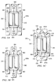
- FIGURES 3A, 3B and 3C illustrate example high power density transistor packages according to embodiments of this disclosure
- FIGURE 5 illustrates physical dimensions of the example high power density transistor package according to the embodiment depicted in FIGURES 3C and 4;
- FIGURE 2 also illustrates various electrical lengths for prior art transistor packages 100.
- the minimum lead length to externally connect a prior art transistor package 100 to a tie point 160 (L Dtie1 ) is approximately 0.670 in.
- FIGURES 3C and 4 illustrate yet another example transistor package 300c according to a third embodiment of this disclosure.
- Transistor package 300c typically houses a power semiconductor having four source (or common) lead 310, 311, 312 and 313, gate (or input) lead 320, and drain (or output) lead 330.
- Transistor package 300c includes package insulator 340 and protective cover 350.
- Transistor package 300c may be 1.0 x 1.0 in. square in dimension, although it could have any other suitable dimensions.
- the leads 310, 311, 312, 313, 320 and 330 may exhibit various sizes and shapes.
- output lead 330 may include: (1) a near end 330a capable of being brazed to package insulator 340; (2) an elongated far end 330b connectable to a tie point 370; and (3) a tapered region 330c between near end 330a and far end 330b. Tapered region 330c may exhibit symmetrically tapered edges as depicted in FIGURE 3C and 4 or other tapered edges. Output lead 330 may have a greater length than that of leads 310 and 311.
- input lead 320 may include: (1) a near end 320a capable of being brazed to package insulator 340; (2) an elongated far end 320b connectable to a tie point; and (3) a tapered region 320c between near end 320a and far end 320b. Tapered region 320c may exhibit symmetrically tapered edges as depicted in FIGURE 3C and 4 or other tapered edges. Input lead 320 may have a greater length than that of leads 312 and 313.
- leads 310, 311, 312, 313, 320 and 330 in transistor package 300c may be soldered to a PCB with tin lead (SnPb) solder and brazed to the package insulator 340 with copper silver (CuAg) brazing.
- Leads 310, 311, 312, 313, 320 and 330 may also include at least one solder lock 360. Each solder lock 360 may be strategically placed to improve surface contact of leads 310, 311, 312, 313, 320 and 330 to the PCB and to increase the periphery of transistor package 300c, thereby adding mechanical strength at the interface of the leads 310, 311, 312, 313, 320 and 330 to the PCB.
- Transistor package 300c decreases, for example, the relative electrical length between adjacent transistor packages by approximately 30%.
- the resulting decrease in physical length for transistor package 300c contributes proportionally to a decrease in inductance, thereby presenting less impedance to the flow of electrical current as the operating frequency increases.
- transistor package 300b the physical lengths are relative to the distance one device is situated from the adjacent device, but the distance between each device may be dictated by a design specification.
- Optimizing or decreasing the physical length or electrical path between two transistor packages may also help to improve frequency response.
- Optimizing lead layout in accordance with the present disclosure reduces, for example, the electrical length by placing external circuitry physically closer to the transistor contacts.
- transistor packages 300b and 300c, in accordance with the present disclosure may substantially increase frequency response when compared to known configurations.
- Optimizing or increasing the edge periphery of transistor lead frames may also generally increase reliability.
- Transistor packages 300a, 300b and 300c exhibit a periphery greater than that of prior art transistor package 100.
- the addition of soldering locks 360 also contributes to greater lead periphery.
- the mechanical strength of the solder and braze joints is increased, thereby improving reliability.
- the improved lead design provides improved surface contact by reducing the occurrence of voiding. Voiding typically occurs when attaching lead frames to the PCB during solder reflow operations. During such reflow operations, entrapped materials (such as flux) easily flow when solder is in a liquid state to regions of less compression and less surface tension (such as those now facilitated by the solder locks) in accordance with an embodiment of this disclosure.
- Transistor packages 300a, 300b, 300c and other transistor packages in accordance with the present disclosure may be used in a variety of applications, such as high power amplifiers. There are several advantages to the use of transistor packages in accordance with the present disclosure over prior art transistor packages.
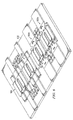
- FIGURE 6 depicts two prior art transistor packages 100 and two transistor packages 300c according to one embodiment of this disclosure mounted on a PCB 600 in a typical application.
- FIGURE 6 indeed illustrates, for example, that the physical electrical length between adjacent transistor packages 300c is decreased when compared to the same of prior art transistors 100. Thus, overall inductance in the system is decreased, thereby improving the frequency response of the system.
- FIGURE 7 illustrates an example method 700 of using the high power density transistor packages 300a, 300b and 300c according to one embodiment of this disclosure.
- the process may begin in Step 710 by choosing a configuration of the leads of a transistor package for a given application. For example, if a given application requires both increased mechanical strength and improved frequency response over that of the prior art, a configuration similar to transistor package 300b or 300c may be chosen. Designers concerned with increasing only the mechanical strength may opt for a configuration similar to transistor package 300a.
- Method 700 may thus continue by placing two transistors (with, for example, transistor package 300b or 300c) adjacent to one another on a PCB in Step 720. Also in step 720, a designer may strategize the configuration of the lead geometries to achieve certain application goals and to optionally improve the overall frequency response of the system. In Step 730, a designer may strategize the number and placement of solder locks as desired for a given application. Step 740 may include soldering a portion of the transistor packages' lead periphery to a PCB to increase mechanical strength and reliability.
- Step 750 may include soldering a portion of a solder lock onto the PCB to further increase mechanical strength and reliability.
- Step 760 may include brazing a portion of the transistor lead periphery to a transistor package insulator, thus further increasing mechanical strength and reliability.
- method 700 may include brazing a portion of the solder lock to the transistor package insulator to further improve the mechanical strength and reliability of the transistor in Step 770.
- the above-referenced steps may be conducted in any order or repeated for any number of transistors as desired.
- Couple and its derivatives refer to any direct or indirect communication between two or more elements, whether or not those elements are in physical contact with one another.
- the term “or” is inclusive, meaning and/or.
- the phrases “associated with” and “associated therewith,” as well as derivatives thereof, may mean to include, be included within, interconnect with, contain, be contained within, connect to or with, couple to or with, be communicable with, cooperate with, interleave, juxtapose, be proximate to, be bound to or with, have, have a property of, or the like.
Landscapes
- Engineering & Computer Science (AREA)
- Manufacturing & Machinery (AREA)
- Microelectronics & Electronic Packaging (AREA)
- Lead Frames For Integrated Circuits (AREA)
- Structures For Mounting Electric Components On Printed Circuit Boards (AREA)
- Multi-Conductor Connections (AREA)
Abstract
Description
- This patent application claims priority under 35 U.S.C. § 119(e) to
U.S. Provisional Patent Application No. 60/680,727 entitled "Improved Reliability and Improved Frequency Response Package for Extremely High Power Density Transistors" filed on May 13, 2005, which is hereby incorporated by reference. - This disclosure is generally directed to high power density transistors and more specifically to systems and methods for increasing the periphery of device leads while improving frequency response.
- It is well known in the field of high frequency design that semiconductor packaging necessarily introduces parasitic inductance by virtue of electrical connections between a semiconductor chip and outside circuitry. The connections are normally formed of wirebonds and conductive traces that collectively pass electrical current from the inside of the package to external leads.
- Due to the extreme high power density of certain transistors, thermal and electrical stress results in eventual mechanical fatigue and ultimately failure of one or both critical interfaces to which lead frame conductors are attached. Such failures result in degraded performance and possibly destruction of the semiconductor. At the same time, in practice it is also often necessary to minimize parasitic inductance in order to maximize the operating frequency capability of the overall structure. Parasitic inductance, which is electrically connected in series with the flow of electrical current, forms a low-pass filter network that tends to oppose the flow of current as the operating frequency increases. At some frequency, determined by the application, the impedance to current flow reaches a critical point at which there is a detrimental impact on system performance. It is often necessary to mitigate the effects of various elements in the electrical path in order to optimize the overall parasitic inductance and increase the maximum operating frequency of the system.
- This disclosure provides a system and method improved reliability and improved frequency response package for extremely high power density transistors.
- In a first embodiment, a high power density transistor structure includes a transistor package capable of housing a high power density transistor. The transistor package has a package insulator and a plurality of transistor leads. Each of the transistor leads has a far end, a near end and a lead periphery. A solder lock is located on at least one of the transistor leads. At least a portion of the solder lock is attachable to a printed circuit board (PCB). At least a portion of the lead periphery of each transistor lead is attachable to at least one of the PCB and the package insulator.
- In a second embodiment, a method for increasing frequency response and mechanical integrity of a high power density transistor having a plurality of leads includes: soldering a portion of a transistor lead periphery of at least one of the leads to a printed circuit board (PCB), soldering a portion of a solder lock of at least one of the leads onto the PCB, and brazing a portion of the transistor lead periphery of at least one of the leads to a transistor package insulator.
- In a third embodiment, a high power density transistor structure includes a first transistor package capable of housing a first high power density transistor and a second transistor package capable of housing a second high power density transistor. The first transistor package has a first package insulator and a plurality of first transistor leads, and the second transistor package has a second package insulator and a plurality of second transistor leads. Each of the transistor leads has a far end, a near end and a lead periphery. The far end of at least one transistor lead has a width greater than a width of the near end of the transistor lead. The transistors are electrically connected by the far ends of at least one lead from the first transistor package and at least one lead from the second transistor package.
- Other technical features may be readily apparent to one skilled in the art from the following figures, descriptions and claims.
- For a more complete understanding of this disclosure and its features, reference is now made to the following description, taken in conjunction with the accompanying drawings, in which:
- FIGURE 1 illustrates an example high power density transistor package of the prior art;
- FIGURE 2 illustrates the physical dimensions of the example high power density transistor package of the prior art depicted in FIGURE 1;
- FIGURES 3A, 3B and 3C illustrate example high power density transistor packages according to embodiments of this disclosure;
- FIGURE 4 illustrates the example high power density transistor package depicted in FIGURE 3C;
- FIGURE 5 illustrates physical dimensions of the example high power density transistor package according to the embodiment depicted in FIGURES 3C and 4;
- FIGURE 6 illustrates an example application for a high power density transistor package according to one embodiment of this disclosure; and
- FIGURE 7 illustrates an example method of using a high power density transistor package according to one embodiment of this disclosure.
- FIGURE 1 illustrates an example high power
density transistor package 100 of the prior art having four source (or common) leads 110, 111, 112 and 113, gate (or input)lead 120 and drain (or output)lead 130. Eachlead transistor package 100, regardless of whethertransistor package 100 is, for example, for a bipolar transistor or a MOSFET.Transistor package 100 includespackage insulator 140, upon which the transistor is attached, andprotective cover 150.Protective cover 150 serves to protect components insidetransistor package 100. In some cases, transistor leads 110, 111, 112, 113, 120 and 130 are soldered to a printed circuit board (PCB) and brazed to thepackage insulator 140. Priorart transistor packages 100 are generally 1.0 x 1.0 inch (in.) square in dimension, while leads 110, 111, 112, 113, 120 and 130 have an elongated, rectangular shape of the same size and dimension. Thecomplete transistor package 100 is normally mechanically attached to a heat spreader by means of the back surface ofpackage insulator 140. - In practice, many applications require two high power
density transistor packages 100 be placed adjacent to one another on a PCB, such that the electrical length between the two is minimized. FIGURE 2 illustrates the physical dimensions and relative proximity of two adjacently placed priorart transistor packages 100. The distance (Dmid1) between the centers of the output leads 130 of the twopackages 100 is approximately 1.210 in. In practice, most prior art high powerdensity transistor packages 100 typically require that a standard periphery lead length be available for soldering and brazing. For example, PDlead, which designates the length of the edge periphery of output lead 130 (or input lead 120) available for soldering to the PCB, is approximately equal to 1.235 in. On the other hand, PDbraze, which designates the length of the edge periphery of output lead 130 (or input lead 120) available for brazing topackage insulator 140, is approximately equal to 0.445 in. In addition, Psleaa, which designates the combined lengths of the edge peripheries ofcommon leads common leads package insulator 140, is approximately equal to 4.230 in. - FIGURE 2 also illustrates various electrical lengths for prior
art transistor packages 100. Taking into account any spacing prerequisites, the minimum lead length to externally connect a priorart transistor package 100 to a tie point 160 (LDtie1) is approximately 0.670 in. Thus, the electrical length between output leads 130 (i.e., the total path length required to connectoutput lead 130 of the first transistor package to theoutput lead 130 of the second transistor package, LDLFAD1) is determined using Equation 1:
- FIGURE 3A depicts
transistor package 300a in accordance with a first embodiment of this disclosure.Transistor package 300a typically houses a power semiconductor having four source (or common) leads 310, 311, 312 and 313, gate (or input)lead 320, and drain (or output)lead 330.Transistor package 300a also includespackage insulator 340 andprotective cover 350.Transistor package 300a may be 1.0 x 1.0 in. square in dimension, although it could have any other suitable dimensions. Eachlead leads package insulator 340 with copper silver (CuAg) brazing. Eachlead solder lock 360 may be strategically placed to improve the surface contact ofleads transistor package 300a, thereby adding mechanical strength at the interface ofleads leads insulator 340 may be gained by redistributing and reducing mechanical stresses. Thus, the reliability oftransistor package 300a is also improved. In addition, improvements in high power density applications, where high power dissipation results in thermal cycling of the entire assembly and exhibits severe mechanical stress upon the soldered and brazed lead frame interfaces, are also achieved. - FIGURE 3B depicts
transistor package 300b in accordance with a second embodiment of this disclosure.Transistor package 300b typically houses a power semiconductor having four source (or common) leads 310, 311, 312 and 313, gate (or input)lead 320, and drain (or output)lead 330.Transistor package 300b includespackage insulator 340 andprotective cover 350.Transistor package 300b may be 1.0 x 1.0 in. square in dimension, although it could have any other suitable dimensions. Eachlead case input lead 320 andoutput lead 330, may be configured to be slightly longer in length than the other leads 310-313. The periphery ofleads package insulator 340 with copper silver (CuAg) brazing.Leads solder lock 360. Eachsolder lock 360 may be strategically placed to improve surface contact ofleads transistor package 300b, thereby adding mechanical strength at the interface of theleads leads package insulator 340 is gained by redistributing and reducing mechanical stresses. Thus, the reliability oftransistor package 300b is also improved. In addition, improvements in high power density applications, where high power dissipation results in thermal cycling of the entire assembly and exhibits severe mechanical stress upon the soldered and brazed lead frame interfaces, are also achieved. - FIGURES 3C and 4 illustrate yet another
example transistor package 300c according to a third embodiment of this disclosure.Transistor package 300c typically houses a power semiconductor having four source (or common)lead lead 320, and drain (or output)lead 330.Transistor package 300c includespackage insulator 340 andprotective cover 350.Transistor package 300c may be 1.0 x 1.0 in. square in dimension, although it could have any other suitable dimensions. In this example, theleads output lead 330 may include: (1) anear end 330a capable of being brazed to packageinsulator 340; (2) an elongatedfar end 330b connectable to atie point 370; and (3) a taperedregion 330c betweennear end 330a andfar end 330b.Tapered region 330c may exhibit symmetrically tapered edges as depicted in FIGURE 3C and 4 or other tapered edges.Output lead 330 may have a greater length than that ofleads - Similarly,
input lead 320 may include: (1) anear end 320a capable of being brazed to packageinsulator 340; (2) an elongatedfar end 320b connectable to a tie point; and (3) a taperedregion 320c betweennear end 320a andfar end 320b.Tapered region 320c may exhibit symmetrically tapered edges as depicted in FIGURE 3C and 4 or other tapered edges.Input lead 320 may have a greater length than that ofleads - The periphery of
leads transistor package 300c may be soldered to a PCB with tin lead (SnPb) solder and brazed to thepackage insulator 340 with copper silver (CuAg) brazing.Leads solder lock 360. Eachsolder lock 360 may be strategically placed to improve surface contact ofleads transistor package 300c, thereby adding mechanical strength at the interface of theleads leads package insulator 340 is gained by redistributing and reducing mechanical stresses. Thus, the reliability oftransistor package 300c is also improved. In addition, improvements in high power density applications, where high power dissipation results in thermal cycling of the entire assembly and exhibits severe mechanical stress upon the soldered and brazed lead frame interfaces, are also achieved. - In practice, applications may require that two high power
density transistor packages 300c be electrically connected (i.e., perhaps in parallel) and placed adjacent to one another as closely as is physically possible on a PCB. FIGURE 5 illustrates the physical dimensions and relative proximity of two adjacently placed high powerdensity transistor packages 300c. The distance (Dmid2) between the centers of the output leads 330 of the twotransistor packages 300c (i.e., X + Y + X) is approximately 1.279 in. (where X is 0.358 in. and Y is 0.563 in.). Taking into account any spacing requirements, the minimum lead length to externally connect a high powerdensity transistor package 300c to a tie point 370 (LDtie2) is approximately 0.259 in. Thus, the total path length (LDlead2) required to connect theoutput lead 330 of afirst transistor package 300c to the output lead of asecond transistor package 300c is determined using Equation 2:
- TABLE 1 below summarizes the pertinent electrical paths and periphery lengths for both prior
art transistor package 100 andtransistor package 300c.TABLE 1 Length Prior Art Transistor Package 100 (inches) Transistor Package 300c (inches)Optimization (percentage) LDlead 2.550 1.797 -29.5% PDlead 1.235 2.807 +127% PDbraze 0.445 0.534 +20% PSlead 4.760 4.280 -10% PSbraze 4.230 4.944 +18% - As shown in TABLE 1, the minimum lead length to externally connect a device to an adjacent device using
transistor package 300c is LDlead2 = 1.797 in. compared to LDlead1 = 2.550 in. for priorart transistor package 100.Transistor package 300c decreases, for example, the relative electrical length between adjacent transistor packages by approximately 30%. The resulting decrease in physical length fortransistor package 300c contributes proportionally to a decrease in inductance, thereby presenting less impedance to the flow of electrical current as the operating frequency increases. The same holds true fortransistor package 300b. Of course, the physical lengths are relative to the distance one device is situated from the adjacent device, but the distance between each device may be dictated by a design specification. - Optimizing or decreasing the physical length or electrical path between two transistor packages may also help to improve frequency response. Optimizing lead layout in accordance with the present disclosure reduces, for example, the electrical length by placing external circuitry physically closer to the transistor contacts. Thus, for example, transistor packages 300b and 300c, in accordance with the present disclosure, may substantially increase frequency response when compared to known configurations.
- Optimizing or increasing the edge periphery of transistor lead frames may also generally increase reliability.
Transistor packages art transistor package 100. The addition ofsoldering locks 360 also contributes to greater lead periphery. The total length of the edge periphery ofoutput lead 330 available for soldering, which includes the additional length gained by the total contribution of corresponding solder locks, is PDlead= 2.807 in., a 127% increase over the priorart transistor package 100. The same holds approximately true forinput lead 320. Thus, the mechanical strength of the solder and braze joints is increased, thereby improving reliability. In addition to increasing the edge periphery, the improved lead design provides improved surface contact by reducing the occurrence of voiding. Voiding typically occurs when attaching lead frames to the PCB during solder reflow operations. During such reflow operations, entrapped materials (such as flux) easily flow when solder is in a liquid state to regions of less compression and less surface tension (such as those now facilitated by the solder locks) in accordance with an embodiment of this disclosure. -
Transistor packages transistor packages 300c according to one embodiment of this disclosure mounted on aPCB 600 in a typical application. FIGURE 6 indeed illustrates, for example, that the physical electrical length betweenadjacent transistor packages 300c is decreased when compared to the same ofprior art transistors 100. Thus, overall inductance in the system is decreased, thereby improving the frequency response of the system. - FIGURE 7 illustrates an
example method 700 of using the high powerdensity transistor packages Step 710 by choosing a configuration of the leads of a transistor package for a given application. For example, if a given application requires both increased mechanical strength and improved frequency response over that of the prior art, a configuration similar totransistor package transistor package 300a. - A given application may require transistors to be placed in parallel with one another, effectively doubling the power available from an amplifier. In such cases, the application generally requires that the distance between adjacent transistors be minimized to improve the overall frequency response.
Method 700 may thus continue by placing two transistors (with, for example,transistor package Step 720. Also instep 720, a designer may strategize the configuration of the lead geometries to achieve certain application goals and to optionally improve the overall frequency response of the system. InStep 730, a designer may strategize the number and placement of solder locks as desired for a given application. Step 740 may include soldering a portion of the transistor packages' lead periphery to a PCB to increase mechanical strength and reliability. Step 750 may include soldering a portion of a solder lock onto the PCB to further increase mechanical strength and reliability. Continuing on in accordance with the present disclosure,Step 760 may include brazing a portion of the transistor lead periphery to a transistor package insulator, thus further increasing mechanical strength and reliability. Finally,method 700 may include brazing a portion of the solder lock to the transistor package insulator to further improve the mechanical strength and reliability of the transistor inStep 770. The above-referenced steps may be conducted in any order or repeated for any number of transistors as desired. - With the above understanding and goals, it is possible to optimize a geometry where similar results could be obtained but are within the scope of this disclosure. For example, although descriptions for
transistor packages - It may be advantageous to set forth definitions of certain words and phrases used in this patent document. The term "couple" and its derivatives refer to any direct or indirect communication between two or more elements, whether or not those elements are in physical contact with one another. The terms "include" and "comprise," as well as derivatives thereof, mean inclusion without limitation. The term "or" is inclusive, meaning and/or. The phrases "associated with" and "associated therewith," as well as derivatives thereof, may mean to include, be included within, interconnect with, contain, be contained within, connect to or with, couple to or with, be communicable with, cooperate with, interleave, juxtapose, be proximate to, be bound to or with, have, have a property of, or the like.
- While this disclosure has described certain embodiments and generally associated methods, alterations and permutations of these embodiments and methods will be apparent to those skilled in the art. Accordingly, the above description of example embodiments does not define or constrain this disclosure. Other changes, substitutions, and alterations are also possible without departing from the spirit and scope of this disclosure, as defined by the following claims.
Claims (16)
- A high power density transistor structure comprising:a transistor package capable of housing a high power density transistor, the transistor package having a package insulator and a plurality of transistor leads, wherein each of the transistor leads has a far end, a near end and a lead periphery; anda solder lock located on at least one of the transistor leads, wherein at least a portion of the solder lock is attachable to a printed circuit board (PCB);wherein at least a portion of the lead periphery of each transistor lead is attachable to at least one of:the PCB; andthe package insulator.
- The transistor structure of Claim 1, wherein the far end of at least one transistor lead has a width approximately equal to or greater than a width of the near end of the transistor lead.
- The transistor structure of Claim 1 or 2, wherein at least one of the transistor leads has a length equal to or greater than a length of at least one other transistor lead.
- The transistor structure of any preceding Claim, wherein at least a portion of the transistor lead periphery of at least one transistor lead is soldered to the PCB, or brazed to the package insulator.
- The transistor structure of any preceding Claim, wherein at least a portion of the solder lock is attachable to the package insulator.
- The transistor structure of Claim 5, wherein the solder lock is brazed to the package insulator.
- The transistor structure of any preceding Claim, wherein the transistor is used in a high power amplifier.
- The transistor structure of any preceding Claim, further comprising a plurality of solder locks of different shapes.
- A method for increasing frequency response and mechanical integrity of a high power density transistor having a plurality of leads, the method comprising:soldering a portion of a transistor lead periphery of at least one of the leads to a printed circuit board (PCB);soldering a portion of a solder lock of at least one of the leads onto the PCB; andbrazing a portion of the transistor lead periphery of at least one of the leads to a transistor package insulator.
- The method of Claim 9, further comprising brazing a portion of the solder lock to the transistor package insulator.
- The method of Claim 9 or 10, wherein each lead has a near end and a far end.
- The method of Claim 11, wherein the far end of at least one transistor lead has a width approximately equal to or greater than a width of the near end of the transistor lead.
- The method of Claim 11 or 12, wherein a length of at least one transistor lead is greater than a length of at least one other transistor lead.
- The method of any of preceding Claims 9 to 13, wherein at least one of:a width of a far end of a first of the transistor leads is greater than a width of a near end of the first transistor lead; anda width of a far end of a second of the transistor leads is greater than a width of a near end of the second transistor lead.
- The method of any of Claims 9 to 14, further comprising at least one of:brazing the solder lock to the package insulator; andbrazing the lead periphery of at least one of the leads to the package insulator.
- A high power density transistor structure comprising:a first transistor package capable of housing a first high power density transistor, the first transistor package having a first package insulator and a plurality of first transistor leads; anda second transistor package capable of housing a second high power density transistor, the second transistor package having a second package insulator and a plurality of second transistor leads;wherein each of the first and second transistor leads has a far end, a near end and a lead periphery, the far end of at least one transistor lead having a width greater than a width of the near end of the transistor lead; andwherein the transistors are electrically connected by the far ends of at least one lead from the first transistor package and at least one lead from the second transistor package.
Applications Claiming Priority (2)
| Application Number | Priority Date | Filing Date | Title |
|---|---|---|---|
| US68072705P | 2005-05-13 | 2005-05-13 | |
| US11/263,115 US20060255455A1 (en) | 2005-05-13 | 2005-10-31 | Reliability and improved frequency response package for extremely high power density transistors |
Publications (2)
| Publication Number | Publication Date |
|---|---|
| EP1722414A2 true EP1722414A2 (en) | 2006-11-15 |
| EP1722414A3 EP1722414A3 (en) | 2008-12-24 |
Family
ID=36818391
Family Applications (1)
| Application Number | Title | Priority Date | Filing Date |
|---|---|---|---|
| EP06251749A Withdrawn EP1722414A3 (en) | 2005-05-13 | 2006-03-30 | Improved reliability and improved frequency response package for extremely high power density transistors |
Country Status (2)
| Country | Link |
|---|---|
| US (1) | US20060255455A1 (en) |
| EP (1) | EP1722414A3 (en) |
Families Citing this family (3)
| Publication number | Priority date | Publication date | Assignee | Title |
|---|---|---|---|---|
| US8639373B2 (en) * | 2009-10-14 | 2014-01-28 | Stmicroelectronics, Inc. | Modular low stress package technology |
| US8597984B2 (en) | 2009-10-14 | 2013-12-03 | Stmicroelectronics, Inc. | Modular low stress package technology |
| US8853843B2 (en) | 2009-10-14 | 2014-10-07 | Stmicroelectronics, Inc. | Modular low stress package technology |
Family Cites Families (6)
| Publication number | Priority date | Publication date | Assignee | Title |
|---|---|---|---|---|
| US5001545A (en) * | 1988-09-09 | 1991-03-19 | Motorola, Inc. | Formed top contact for non-flat semiconductor devices |
| EP0437312B1 (en) * | 1990-01-08 | 1994-10-26 | Nec Corporation | Electronic part mountable on the surface of a printed circuit board and method of mounting the same |
| JPH0555438A (en) * | 1991-08-26 | 1993-03-05 | Rohm Co Ltd | Lead terminal structure of electronic component |
| US5647124A (en) * | 1994-04-25 | 1997-07-15 | Texas Instruments Incorporated | Method of attachment of a semiconductor slotted lead to a substrate |
| TW468258B (en) * | 1998-10-21 | 2001-12-11 | Hitachi Ltd | Semiconductor device and method of manufacturing the same |
| US6891256B2 (en) * | 2001-10-22 | 2005-05-10 | Fairchild Semiconductor Corporation | Thin, thermally enhanced flip chip in a leaded molded package |
-
2005
- 2005-10-31 US US11/263,115 patent/US20060255455A1/en not_active Abandoned
-
2006
- 2006-03-30 EP EP06251749A patent/EP1722414A3/en not_active Withdrawn
Also Published As
| Publication number | Publication date |
|---|---|
| EP1722414A3 (en) | 2008-12-24 |
| US20060255455A1 (en) | 2006-11-16 |
Similar Documents
| Publication | Publication Date | Title |
|---|---|---|
| US11335645B2 (en) | High-frequency module and manufacturing method thereof | |
| US10098229B2 (en) | Module, module component composing the module, and method of manufacturing the module | |
| US20220007499A1 (en) | Module, terminal assembly, and method for producing module | |
| US20020131255A1 (en) | I-channel surface-mount connector | |
| US6657866B2 (en) | Electronics assembly with improved heatsink configuration | |
| JPH07273276A (en) | Connection structure of power element and snubber element and its mounting structure | |
| US20220029262A1 (en) | High powered rf part for improved manufacturability | |
| US20080217770A1 (en) | Mounting configuration of electronic component | |
| US5731960A (en) | Low inductance decoupling capacitor arrangement | |
| EP2398302A1 (en) | Semiconductor module and semiconductor device | |
| JP2014132680A (en) | Electric or electronic device | |
| US6503088B2 (en) | I-channel surface-mount connector with extended flanges | |
| JP2001237570A (en) | Power electronic module and its manufacturing method | |
| US20060255455A1 (en) | Reliability and improved frequency response package for extremely high power density transistors | |
| CN223428630U (en) | Device packaging structure | |
| JPH088372A (en) | Heat dissipation device | |
| US5751555A (en) | Electronic component having reduced capacitance | |
| US4536825A (en) | Leadframe having severable fingers for aligning one or more electronic circuit device components | |
| DE102007005234B4 (en) | Power electronic module with a ceramic enclosure | |
| JPH09307202A (en) | Hybrid integrated circuit | |
| US12402240B2 (en) | Silicon carbide thermal bridge integrated on a low thermal conductivity substrate and processes implementing the same | |
| US20250079383A1 (en) | Semiconductor device | |
| JP2005228811A (en) | Semiconductor device | |
| US9431317B2 (en) | Power doubler amplifier module with improved solder coverage between a heat sink and a thermal pad of a circuit package | |
| US20250364518A1 (en) | Integrated package structure with inductor and integrated circuit and manufacturing method thereof |
Legal Events
| Date | Code | Title | Description |
|---|---|---|---|
| PUAI | Public reference made under article 153(3) epc to a published international application that has entered the european phase |
Free format text: ORIGINAL CODE: 0009012 |
|
| AK | Designated contracting states |
Kind code of ref document: A2 Designated state(s): AT BE BG CH CY CZ DE DK EE ES FI FR GB GR HU IE IS IT LI LT LU LV MC NL PL PT RO SE SI SK TR |
|
| AX | Request for extension of the european patent |
Extension state: AL BA HR MK YU |
|
| PUAL | Search report despatched |
Free format text: ORIGINAL CODE: 0009013 |
|
| AK | Designated contracting states |
Kind code of ref document: A3 Designated state(s): AT BE BG CH CY CZ DE DK EE ES FI FR GB GR HU IE IS IT LI LT LU LV MC NL PL PT RO SE SI SK TR |
|
| AX | Request for extension of the european patent |
Extension state: AL BA HR MK YU |
|
| RIC1 | Information provided on ipc code assigned before grant |
Ipc: H05K 3/34 20060101ALN20081118BHEP Ipc: H01L 23/498 20060101AFI20060828BHEP |
|
| 17P | Request for examination filed |
Effective date: 20090610 |
|
| 17Q | First examination report despatched |
Effective date: 20090803 |
|
| AKX | Designation fees paid |
Designated state(s): DE FR GB IT |
|
| STAA | Information on the status of an ep patent application or granted ep patent |
Free format text: STATUS: THE APPLICATION IS DEEMED TO BE WITHDRAWN |
|
| 18D | Application deemed to be withdrawn |
Effective date: 20091215 |