EP1717899A1 - Antenna structure for operating multi-band system - Google Patents
Antenna structure for operating multi-band system Download PDFInfo
- Publication number
- EP1717899A1 EP1717899A1 EP05018024A EP05018024A EP1717899A1 EP 1717899 A1 EP1717899 A1 EP 1717899A1 EP 05018024 A EP05018024 A EP 05018024A EP 05018024 A EP05018024 A EP 05018024A EP 1717899 A1 EP1717899 A1 EP 1717899A1
- Authority
- EP
- European Patent Office
- Prior art keywords
- radiation metal
- antenna structure
- metal wire
- feed
- wire
- Prior art date
- Legal status (The legal status is an assumption and is not a legal conclusion. Google has not performed a legal analysis and makes no representation as to the accuracy of the status listed.)
- Ceased
Links
- 230000005855 radiation Effects 0.000 claims abstract description 65
- 239000002184 metal Substances 0.000 claims abstract description 59
- 230000008878 coupling Effects 0.000 claims description 6
- 238000010168 coupling process Methods 0.000 claims description 6
- 238000005859 coupling reaction Methods 0.000 claims description 6
- 239000004020 conductor Substances 0.000 claims description 5
- 238000013461 design Methods 0.000 abstract description 4
- 238000004519 manufacturing process Methods 0.000 abstract description 2
- 230000005404 monopole Effects 0.000 description 9
- 238000010586 diagram Methods 0.000 description 6
- 238000004891 communication Methods 0.000 description 4
- 238000002474 experimental method Methods 0.000 description 2
- 230000010354 integration Effects 0.000 description 2
- 238000000034 method Methods 0.000 description 2
- 238000012986 modification Methods 0.000 description 2
- 230000004048 modification Effects 0.000 description 2
- 238000005452 bending Methods 0.000 description 1
- 230000007423 decrease Effects 0.000 description 1
- 238000011161 development Methods 0.000 description 1
- 238000010295 mobile communication Methods 0.000 description 1
- 238000012552 review Methods 0.000 description 1
Images




Classifications
-
- H—ELECTRICITY
- H01—ELECTRIC ELEMENTS
- H01Q—ANTENNAS, i.e. RADIO AERIALS
- H01Q1/00—Details of, or arrangements associated with, antennas
- H01Q1/12—Supports; Mounting means
- H01Q1/22—Supports; Mounting means by structural association with other equipment or articles
- H01Q1/24—Supports; Mounting means by structural association with other equipment or articles with receiving set
- H01Q1/241—Supports; Mounting means by structural association with other equipment or articles with receiving set used in mobile communications, e.g. GSM
- H01Q1/242—Supports; Mounting means by structural association with other equipment or articles with receiving set used in mobile communications, e.g. GSM specially adapted for hand-held use
- H01Q1/243—Supports; Mounting means by structural association with other equipment or articles with receiving set used in mobile communications, e.g. GSM specially adapted for hand-held use with built-in antennas
-
- H—ELECTRICITY
- H01—ELECTRIC ELEMENTS
- H01Q—ANTENNAS, i.e. RADIO AERIALS
- H01Q1/00—Details of, or arrangements associated with, antennas
- H01Q1/36—Structural form of radiating elements, e.g. cone, spiral, umbrella; Particular materials used therewith
- H01Q1/38—Structural form of radiating elements, e.g. cone, spiral, umbrella; Particular materials used therewith formed by a conductive layer on an insulating support
-
- H—ELECTRICITY
- H01—ELECTRIC ELEMENTS
- H01Q—ANTENNAS, i.e. RADIO AERIALS
- H01Q21/00—Antenna arrays or systems
- H01Q21/30—Combinations of separate antenna units operating in different wavebands and connected to a common feeder system
Definitions
- the present invention generally relates to an antenna structure for operating multi-band system, and more particularly relates to a circuit board having a hole for fixing the antenna structure, and further comprising radiation metal wires to correspond with outer spaces for bending suitably.
- the role of antennas in wireless communication devices is to transmit and to receive data of wireless system.
- the antenna design in mobile phones and Personal Digital Assistances (PDA) can be a traditional planner antenna or a monopole antenna and further can be a helical antenna,
- the planner antenna uses a base having dielectric constants for supporting that does not only increase cost but also increases complexity.
- the radiation bandwidth of the planner antenna is not better than the monopole antenna.
- the monopole antenna takes a characteristic with Omni-Directional Radiation Pattern. Referring to FIG. 1, a distribution diagram of an example of omni-directional radiation pattern of a prior art monopole antenna is illustrated.
- the helical antenna is an uncovered structure that suffers damages easily.
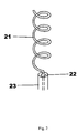
- the helical antenna comprises a helical antenna 21, a feed point 22, and a feed wire 23.
- the helical antenna is used to transmit and to receive signal in a single band.
- the feed wire 23 provides a feed point 22 for coupling the helical antenna 21. Due to the characteristics of mentioned above, there must be a case for containing the monopole antenna.
- wireless communication devices start to do receiving integration in different frequency sections.
- the integration development of the antenna is used to receive wireless signal of different frequency sections and is an application of the wideband antenna. Therefore, the monopole antennas of two different frequency sections are integrated into a wideband antenna that appears in the wireless communication field. Furthermore, there is also a module design for antenna carrier support.
- FIG. 3 a schematic diagram of an example of an antenna carrier support of a prior art wideband antenna is illustrated.
- the wideband of the antenna carrier support comprises an antenna base 31, a feed point 32 a low frequency radiation metal wire 33, and a high frequency radiation metal wire 34.
- the antenna base 31 is used to support the wideband antenna that comprises the low frequency radiation metal wire 33 and the high frequency radiation metal wire 34.
- the antenna base 31 also provides a feed point 32 to couple to the wideband antenna and still has capacity to accept other components.
- the characteristics of mentioned above increase complexity of wireless communication devices and raises costs. There must be some ways to resolve the problem.
- an object of the present invention is to provide an antenna structure for operating multi-band system.
- the antenna structure is applied on a base having at least one hole.
- the antenna structure comprises at least one feed wire that is set on the base to form a feed point and at least one radiation metal wire that is embedded the hole.
- the radiation metal wire has a feed terminal for coupling the feed point.
- the radiation metal wire further has a ground surface that is set on the base and couples to an outer ground conductor of the feed wire.
- the feed wire covered by the outer ground conductor is a feed coaxial transport wire.
- the base can be a circuit board that is composed by any form.
- the hole can be set on the border of the base or into the inside of the base.
- the radiation metal wire has a first radiation metal wire and a second radiation metal wire.
- the feed terminal of the first radiation metal wire couples to the feed point.
- the second radiation metal wire has a start terminal for coupling the first radiation metal wire near the feed terminal.
- the radiation metal wire does not touch with the base except the feed terminal and a touch point is embedded into the hole.
- the radiation metal wire is to extend and to bend freely according to a space formed by a case.
- the length of the first radiation metal wire is bigger than the second radiation metal wire that has a certain length for corresponding with a first operating band in order to receive or send the signal of the first operating band.
- the second radiation metal wire is smaller than the first radiation metal wire that has a certain length for corresponding with a second operating band in order to receive or send the signal of the second operating band.
- the first operating band can be a low frequency operating band and the second operating band can be a high frequency operating band.
- the antenna structure for operating multi-band system comprises a circuit board 41, a first radiation metal wire 42, a second radiation metal wire 43, a feed coaxial transport wire 44, and a ground surface 45.
- the border of the circuit board 41 has at least one hole 411 for embedding the first radiation metal wire 42 and the first radiation metal wire 42 couples to the feed point 441 provided by the feed coaxial transport wire 44.
- the feed coaxial transport wire 44 is composed of the feed wire covering the outer ground conductor.
- the second radiation metal wire 43 couples to the first radiation metal wire 42 near the feed point 441.
- the ground surface 45 is set on the circuit board 41.
- the first radiation metal wire 42 and the second radiation metal wire 43 does not touch the circuit board 41 except fixing into the hole 411 and coupling to the feed point 441.
- the end of both radiation metal wires 42, 43 extend to the same side.
- the first radiation metal wire 42 is to receive and to transmit the low frequency operating band of the first operating band, such as 824-960 MHz.
- the second radiation metal wire 43 is to receive and to send the high frequency operating band of the second operating band, such as 1710-2170 MHz.
- FIG. 6 is an experiment result of a return loss and a voltage standing wave ratio of an antenna structure for operating multi-band system according to an embodiment of the present invention.
- the curve of point 61 to point 62 is the low frequency operating band 824 MHz-960 MHz and the curve of point 63 to point 64 is the high frequency operating band 1710 MHz-2170 MHz. Therefore, the antenna band can cover four bands of GSM (Global System for Mobile Communication) and the band of WCDMA (Wideband Code Division Multiple Access) (824-960 MHz, 1710-2170 MHz). Moreover, the high frequency band can be reached 460 MHz and return loss observation in the low frequency operating band and the high frequency operating band has a better gain of antenna radiation.
- GSM Global System for Mobile Communication
- WCDMA Wideband Code Division Multiple Access
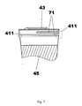
- FIG. 7 a structural drawing of an example of an antenna structure for operating multi-band system according to an embodiment of the present invention is illustrated.
- the first radiation metal wire 71 is to extend from different directions from shown in FIG. 4 and FIG. 5.
- the extended result will take the tail of the first radiation metal wire 71 and the tail of the second radiation metal wire 43 to set at different sides.
- FIG. 8 another structural drawing of an example of an antenna structure for operating multi-band system according to an embodiment of the present invention is illustrated.
- the circuit board 41 is set into a space of a case 84 and there is at least one hole 83 that is set into the circuit board 41 for fixing the first radiation metal wire 81.
- the first radiation metal wire 81 and the second radiation metal wire 82 are to extend according to the space provided by the case 84.
- the antenna structure uses a monopole antenna for setting structure and is hided into the case. Therefore, the advantage of the invention is to satisfy the characteristics with wideband monopole antennas and omni-directional radiation pattern.
- the invention also overcomes the drawback with the uncovered structure.
- the invention of the antenna structure has a better gain of antenna radiation in the low frequency operating band 824 MHz-960MHz and the high frequency operating band 1710 MHz-2170 MHz.
- the invention uses a radiation metal wire to be a main body and uses the hole of the circuit board to fix the antenna.
- the design decreases complexity in the antenna module structure and the antenna is bent by metal wires without antenna carrier supports.
- the characteristics increase the capabilities of production and reduce cost.
- Another advantage of the invention is that the antenna structure can be set any shape of cases. In other words, the antenna structure can be bent freely according to any shape of cases.
- the present invention is novel and useful and definite enhances the performance over the conventional structure and further complies with the patent application requirements and is submitted to the Patent and Trademark Office for review and granting of the commensurate patent rights.
Landscapes
- Engineering & Computer Science (AREA)
- Computer Networks & Wireless Communication (AREA)
- Details Of Aerials (AREA)
- Support Of Aerials (AREA)
- Variable-Direction Aerials And Aerial Arrays (AREA)
Abstract
Description
- The present invention generally relates to an antenna structure for operating multi-band system, and more particularly relates to a circuit board having a hole for fixing the antenna structure, and further comprising radiation metal wires to correspond with outer spaces for bending suitably.
- The role of antennas in wireless communication devices is to transmit and to receive data of wireless system. General speaking, the antenna design in mobile phones and Personal Digital Assistances (PDA) can be a traditional planner antenna or a monopole antenna and further can be a helical antenna, However, the planner antenna uses a base having dielectric constants for supporting that does not only increase cost but also increases complexity. The radiation bandwidth of the planner antenna is not better than the monopole antenna. The monopole antenna takes a characteristic with Omni-Directional Radiation Pattern. Referring to FIG. 1, a distribution diagram of an example of omni-directional radiation pattern of a prior art monopole antenna is illustrated. The helical antenna is an uncovered structure that suffers damages easily.
- Referring to FIG. 2, a schematic diagram of an example of a prior art helical antenna is illustrated. The helical antenna comprises a
helical antenna 21, afeed point 22, and afeed wire 23. The helical antenna is used to transmit and to receive signal in a single band. Thefeed wire 23 provides afeed point 22 for coupling thehelical antenna 21. Due to the characteristics of mentioned above, there must be a case for containing the monopole antenna. - Because of the frequency sections are opened gradually, wireless communication devices start to do receiving integration in different frequency sections. The integration development of the antenna is used to receive wireless signal of different frequency sections and is an application of the wideband antenna. Therefore, the monopole antennas of two different frequency sections are integrated into a wideband antenna that appears in the wireless communication field. Furthermore, there is also a module design for antenna carrier support.
- Referring to FIG. 3, a schematic diagram of an example of an antenna carrier support of a prior art wideband antenna is illustrated. The wideband of the antenna carrier support comprises an
antenna base 31, a feed point 32 a low frequencyradiation metal wire 33, and a high frequencyradiation metal wire 34. Theantenna base 31 is used to support the wideband antenna that comprises the low frequencyradiation metal wire 33 and the high frequencyradiation metal wire 34. Theantenna base 31 also provides afeed point 32 to couple to the wideband antenna and still has capacity to accept other components. However, the characteristics of mentioned above increase complexity of wireless communication devices and raises costs. There must be some ways to resolve the problem. - Therefore, an object of the present invention is to provide an antenna structure for operating multi-band system. The antenna structure is applied on a base having at least one hole. The antenna structure comprises at least one feed wire that is set on the base to form a feed point and at least one radiation metal wire that is embedded the hole. The radiation metal wire has a feed terminal for coupling the feed point. The radiation metal wire further has a ground surface that is set on the base and couples to an outer ground conductor of the feed wire. The feed wire covered by the outer ground conductor is a feed coaxial transport wire. The base can be a circuit board that is composed by any form. The hole can be set on the border of the base or into the inside of the base. The radiation metal wire has a first radiation metal wire and a second radiation metal wire. The feed terminal of the first radiation metal wire couples to the feed point. The second radiation metal wire has a start terminal for coupling the first radiation metal wire near the feed terminal. The radiation metal wire does not touch with the base except the feed terminal and a touch point is embedded into the hole. The radiation metal wire is to extend and to bend freely according to a space formed by a case. In addition, the length of the first radiation metal wire is bigger than the second radiation metal wire that has a certain length for corresponding with a first operating band in order to receive or send the signal of the first operating band. The second radiation metal wire is smaller than the first radiation metal wire that has a certain length for corresponding with a second operating band in order to receive or send the signal of the second operating band. The first operating band can be a low frequency operating band and the second operating band can be a high frequency operating band.
-
- FIG. 1 is a distribution diagram of an example of omni-directional pattern of a prior art monopole antenna;
- FIG. 2 is a schematic diagram of an example of a prior art helical antenna;
- FIG. 3 is a schematic diagram of an example of an antenna carrier support of a prior art wideband antenna;
- FIG. 4 is a lateral view of an example of an antenna structure for operating multi-band system according to an embodiment of the present invention;
- FIG. 5 is a vertical view of an example of an antenna structure for operating multi-band system according to an embodiment of the present invention;
- FIG. 6 is an experiment result of a return loss and a voltage standing wave ratio of an antenna structure for operating multi-band system according to an embodiment of the present invention;
- FIG. 7 is a structural drawing of an example of an antenna structure for operating multi-band system according to an embodiment of the present invention; and
- FIG. 8 is another structural drawing of an example of an antenna structure for operating multi-band system according to an embodiment of the present invention.
- To make it easier for our examiner to understand the objective of the invention, its innovative features and performance, a detailed description and technical characteristics of the present invention are described together with the drawings as follows.
- Referring to FIG. 4 and FIG. 5, a lateral view and a vertical view of examples of an antenna structure for operating multi-band system according to embodiments of the present invention are illustrated. The antenna structure for operating multi-band system comprises a
circuit board 41, a firstradiation metal wire 42, a secondradiation metal wire 43, a feedcoaxial transport wire 44, and aground surface 45. The border of thecircuit board 41 has at least onehole 411 for embedding the firstradiation metal wire 42 and the firstradiation metal wire 42 couples to thefeed point 441 provided by the feedcoaxial transport wire 44. The feedcoaxial transport wire 44 is composed of the feed wire covering the outer ground conductor. The secondradiation metal wire 43 couples to the firstradiation metal wire 42 near thefeed point 441. In addition, theground surface 45 is set on thecircuit board 41. As shown in FIG. 5, the firstradiation metal wire 42 and the secondradiation metal wire 43 does not touch thecircuit board 41 except fixing into thehole 411 and coupling to thefeed point 441. The end of bothradiation metal wires radiation metal wire 42 is to receive and to transmit the low frequency operating band of the first operating band, such as 824-960 MHz. The secondradiation metal wire 43 is to receive and to send the high frequency operating band of the second operating band, such as 1710-2170 MHz. FIG. 6 is an experiment result of a return loss and a voltage standing wave ratio of an antenna structure for operating multi-band system according to an embodiment of the present invention. The curve of point 61 to point 62 is the low frequency operating band 824 MHz-960 MHz and the curve ofpoint 63 topoint 64 is the high frequency operating band 1710 MHz-2170 MHz. Therefore, the antenna band can cover four bands of GSM (Global System for Mobile Communication) and the band of WCDMA (Wideband Code Division Multiple Access) (824-960 MHz, 1710-2170 MHz). Moreover, the high frequency band can be reached 460 MHz and return loss observation in the low frequency operating band and the high frequency operating band has a better gain of antenna radiation. - Referring to FIG. 7, a structural drawing of an example of an antenna structure for operating multi-band system according to an embodiment of the present invention is illustrated. The first
radiation metal wire 71 is to extend from different directions from shown in FIG. 4 and FIG. 5. The extended result will take the tail of the firstradiation metal wire 71 and the tail of the secondradiation metal wire 43 to set at different sides. - In addition, referring to FIG. 8, another structural drawing of an example of an antenna structure for operating multi-band system according to an embodiment of the present invention is illustrated. The
circuit board 41 is set into a space of acase 84 and there is at least onehole 83 that is set into thecircuit board 41 for fixing the firstradiation metal wire 81. The firstradiation metal wire 81 and the secondradiation metal wire 82 are to extend according to the space provided by thecase 84. - As mentioned above, the antenna structure uses a monopole antenna for setting structure and is hided into the case. Therefore, the advantage of the invention is to satisfy the characteristics with wideband monopole antennas and omni-directional radiation pattern. The invention also overcomes the drawback with the uncovered structure. The invention of the antenna structure has a better gain of antenna radiation in the low frequency operating band 824 MHz-960MHz and the high frequency operating band 1710 MHz-2170 MHz. In the apparatus characteristics, the invention uses a radiation metal wire to be a main body and uses the hole of the circuit board to fix the antenna. The design decreases complexity in the antenna module structure and the antenna is bent by metal wires without antenna carrier supports. The characteristics increase the capabilities of production and reduce cost. Another advantage of the invention is that the antenna structure can be set any shape of cases. In other words, the antenna structure can be bent freely according to any shape of cases.
- While the invention has been described by way of example and in terms of a preferred embodiment, it is to be understood that the invention is not limited thereto. To the contrary, it is intended to cover various modifications and similar arrangements and procedures, and the scope of the appended claims therefore should be accorded the broadest interpretation so as to encompass all such modifications and similar arrangements and procedures.
- In summation of the description above, the present invention is novel and useful and definite enhances the performance over the conventional structure and further complies with the patent application requirements and is submitted to the Patent and Trademark Office for review and granting of the commensurate patent rights.
Claims (11)
- An antenna structure, applying on a base having at least one hole, at least comprising:a feed wire, being set on said base and being formed a feed point; andat least one radiation metal wire, being embedded into said hole and having a feed terminal for coupling said feed point.
- The antenna structure of claim 1, wherein said antenna structure further comprises a ground surface that is set on said base and couples to an outer ground conductor of said feed wire.
- The antenna structure of claim 1, wherein said base is a circuit board.
- The antenna structure of claim 1, wherein the extension direction of said radiation metal wire bends freely according to a space, and does not touch with said base except said feed terminal and a touch point is fixed in said hole.
- The antenna structure of claim 4, wherein said space is formed by a case.
- The antenna structure of claim 1, wherein said radiation metal wire has a first radiation metal wire and a second radiation metal; wherein said feed terminal of said first radiation metal couples to said feed point, said second radiation metal has a start terminal for coupling said first radiation metal wire near said feed terminal.
- The antenna structure of claim 6, wherein said first radiation metal wire applies to a first operating band, has a certain length for corresponding with said first operating band, and the length is bigger than said second radiation metal wire.
- The antenna structure of claim 7, wherein said first operating band is a low frequency operating band.
- The antenna structure of claim 6, wherein said second radiation wire applies to a second operating band, has a certain length for corresponding with said second operating band, and the length is smaller than said first radiation metal wire.
- The antenna structure of claim 9, wherein said second operating band is a high frequency operating band.
- The antenna structure of claim 1, wherein said feed point is a feed coaxial transport wire, the composing of said feed coaxial transport wire is that said outer ground conductor covers said feed wire.
Applications Claiming Priority (1)
| Application Number | Priority Date | Filing Date | Title |
|---|---|---|---|
| CNB2005100678576A CN100511836C (en) | 2005-04-29 | 2005-04-29 | Antenna structure suitable for multi-frequency system operation |
Publications (1)
| Publication Number | Publication Date |
|---|---|
| EP1717899A1 true EP1717899A1 (en) | 2006-11-02 |
Family
ID=35353164
Family Applications (1)
| Application Number | Title | Priority Date | Filing Date |
|---|---|---|---|
| EP05018024A Ceased EP1717899A1 (en) | 2005-04-29 | 2005-08-19 | Antenna structure for operating multi-band system |
Country Status (2)
| Country | Link |
|---|---|
| EP (1) | EP1717899A1 (en) |
| CN (1) | CN100511836C (en) |
Families Citing this family (2)
| Publication number | Priority date | Publication date | Assignee | Title |
|---|---|---|---|---|
| TWI625000B (en) * | 2013-08-29 | 2018-05-21 | 富智康(香港)有限公司 | Antenna structure and wireless communication device using same |
| CN106058444B (en) * | 2016-07-20 | 2019-06-04 | 北京小鸟看看科技有限公司 | A kind of two-way antenna and a kind of wireless communication device of virtual reality system |
Citations (4)
| Publication number | Priority date | Publication date | Assignee | Title |
|---|---|---|---|---|
| EP0980114A1 (en) * | 1998-08-12 | 2000-02-16 | Sony Corporation | Helical antenna and portable transceiver |
| US20020089453A1 (en) * | 2001-01-10 | 2002-07-11 | Wen-Jen Tseng | Multi-frequency band antenna |
| US20020118134A1 (en) * | 2001-01-02 | 2002-08-29 | Auden Technology Mfg. Co., Ltd. | Planar helix antenna with two frequencies |
| US20020175866A1 (en) * | 2001-05-25 | 2002-11-28 | Gram Hans Erik | Antenna |
Family Cites Families (6)
| Publication number | Priority date | Publication date | Assignee | Title |
|---|---|---|---|---|
| CN2331091Y (en) * | 1998-01-16 | 1999-07-28 | 电子科技大学 | Microwave multiple-frequency modulation receiver-transmitter |
| CN2465339Y (en) * | 2000-12-26 | 2001-12-12 | 耀登科技股份有限公司 | Planar Helical Dual Band Antenna |
| CN1452271A (en) * | 2002-04-19 | 2003-10-29 | 广达电脑股份有限公司 | Built-in multi-frequency antenna |
| CN2558098Y (en) * | 2002-05-27 | 2003-06-25 | 正文科技股份有限公司 | Array type plane antenna |
| US6664931B1 (en) * | 2002-07-23 | 2003-12-16 | Motorola, Inc. | Multi-frequency slot antenna apparatus |
| CN1234191C (en) * | 2002-08-29 | 2005-12-28 | 智邦科技股份有限公司 | Dual frequency dual dipole antenna |
-
2005
- 2005-04-29 CN CNB2005100678576A patent/CN100511836C/en not_active Expired - Lifetime
- 2005-08-19 EP EP05018024A patent/EP1717899A1/en not_active Ceased
Patent Citations (4)
| Publication number | Priority date | Publication date | Assignee | Title |
|---|---|---|---|---|
| EP0980114A1 (en) * | 1998-08-12 | 2000-02-16 | Sony Corporation | Helical antenna and portable transceiver |
| US20020118134A1 (en) * | 2001-01-02 | 2002-08-29 | Auden Technology Mfg. Co., Ltd. | Planar helix antenna with two frequencies |
| US20020089453A1 (en) * | 2001-01-10 | 2002-07-11 | Wen-Jen Tseng | Multi-frequency band antenna |
| US20020175866A1 (en) * | 2001-05-25 | 2002-11-28 | Gram Hans Erik | Antenna |
Also Published As
| Publication number | Publication date |
|---|---|
| CN1694305A (en) | 2005-11-09 |
| CN100511836C (en) | 2009-07-08 |
Similar Documents
| Publication | Publication Date | Title |
|---|---|---|
| JP3775795B1 (en) | Wireless device | |
| US7388543B2 (en) | Multi-frequency band antenna device for radio communication terminal having wide high-band bandwidth | |
| EP1750323A1 (en) | Multi-band antenna device for radio communication terminal and radio communication terminal comprising the multi-band antenna device | |
| US7541984B2 (en) | Multiple frequency band antenna | |
| US9397405B2 (en) | Antenna device | |
| US20100123628A1 (en) | Multi-Band Antenna | |
| US7659866B1 (en) | Multiple frequency band antenna | |
| US7450076B1 (en) | Integrated multi-band antenna | |
| CN112448156A (en) | Antenna structure | |
| EP2610967A1 (en) | Communication device and antenna structure therein | |
| CN114389019B (en) | Antenna System | |
| US7557759B2 (en) | Integrated multi-band antenna | |
| CN102055061B (en) | Multi-frequency mobile communication device and its antenna | |
| US7391375B1 (en) | Multi-band antenna | |
| US7053839B2 (en) | Antenna for a portable communication apparatus, and a portable communication apparatus comprising such an antenna | |
| US7904126B2 (en) | Antenna applied to slide type mobile communication terminal | |
| EP1318566B1 (en) | Dual-frequency antenna | |
| CN101364671A (en) | Multiband antenna device | |
| US7193566B2 (en) | Planar monopole antennas | |
| US7542002B1 (en) | Wideband monopole antenna | |
| EP2242143A1 (en) | Antenna with increased electrical length and wireless communication device including the same | |
| US7495617B2 (en) | Multi-band antenna | |
| CN101505000A (en) | Multi-frequency band antenna and wireless communication terminal using the same | |
| US8797215B2 (en) | Wire antenna | |
| CN101783439B (en) | multi-frequency antenna |
Legal Events
| Date | Code | Title | Description |
|---|---|---|---|
| PUAI | Public reference made under article 153(3) epc to a published international application that has entered the european phase |
Free format text: ORIGINAL CODE: 0009012 |
|
| AK | Designated contracting states |
Kind code of ref document: A1 Designated state(s): AT BE BG CH CY CZ DE DK EE ES FI FR GB GR HU IE IS IT LI LT LU LV MC NL PL PT RO SE SI SK TR |
|
| AX | Request for extension of the european patent |
Extension state: AL BA HR MK YU |
|
| 17P | Request for examination filed |
Effective date: 20070411 |
|
| 17Q | First examination report despatched |
Effective date: 20070516 |
|
| AKX | Designation fees paid |
Designated state(s): DE FR GB |
|
| RAP1 | Party data changed (applicant data changed or rights of an application transferred) |
Owner name: HTC CORPORATION |
|
| STAA | Information on the status of an ep patent application or granted ep patent |
Free format text: STATUS: THE APPLICATION HAS BEEN REFUSED |
|
| 18R | Application refused |
Effective date: 20091019 |