EP1717731A1 - Radio frequency IC tag and method for manufacturing same - Google Patents
Radio frequency IC tag and method for manufacturing same Download PDFInfo
- Publication number
- EP1717731A1 EP1717731A1 EP05257749A EP05257749A EP1717731A1 EP 1717731 A1 EP1717731 A1 EP 1717731A1 EP 05257749 A EP05257749 A EP 05257749A EP 05257749 A EP05257749 A EP 05257749A EP 1717731 A1 EP1717731 A1 EP 1717731A1
- Authority
- EP
- European Patent Office
- Prior art keywords
- antenna
- radio frequency
- spacer
- case
- tag
- Prior art date
- Legal status (The legal status is an assumption and is not a legal conclusion. Google has not performed a legal analysis and makes no representation as to the accuracy of the status listed.)
- Granted
Links
Images


Classifications
-
- H—ELECTRICITY
- H01—ELECTRIC ELEMENTS
- H01Q—ANTENNAS, i.e. RADIO AERIALS
- H01Q19/00—Combinations of primary active antenna elements and units with secondary devices, e.g. with quasi-optical devices, for giving the antenna a desired directional characteristic
- H01Q19/22—Combinations of primary active antenna elements and units with secondary devices, e.g. with quasi-optical devices, for giving the antenna a desired directional characteristic using a secondary device in the form of a single substantially straight conductive element
-
- G—PHYSICS
- G06—COMPUTING OR CALCULATING; COUNTING
- G06K—GRAPHICAL DATA READING; PRESENTATION OF DATA; RECORD CARRIERS; HANDLING RECORD CARRIERS
- G06K19/00—Record carriers for use with machines and with at least a part designed to carry digital markings
- G06K19/06—Record carriers for use with machines and with at least a part designed to carry digital markings characterised by the kind of the digital marking, e.g. shape, nature, code
- G06K19/067—Record carriers with conductive marks, printed circuits or semiconductor circuit elements, e.g. credit or identity cards also with resonating or responding marks without active components
- G06K19/07—Record carriers with conductive marks, printed circuits or semiconductor circuit elements, e.g. credit or identity cards also with resonating or responding marks without active components with integrated circuit chips
- G06K19/077—Constructional details, e.g. mounting of circuits in the carrier
- G06K19/07749—Constructional details, e.g. mounting of circuits in the carrier the record carrier being capable of non-contact communication, e.g. constructional details of the antenna of a non-contact smart card
-
- G—PHYSICS
- G06—COMPUTING OR CALCULATING; COUNTING
- G06K—GRAPHICAL DATA READING; PRESENTATION OF DATA; RECORD CARRIERS; HANDLING RECORD CARRIERS
- G06K19/00—Record carriers for use with machines and with at least a part designed to carry digital markings
- G06K19/06—Record carriers for use with machines and with at least a part designed to carry digital markings characterised by the kind of the digital marking, e.g. shape, nature, code
- G06K19/067—Record carriers with conductive marks, printed circuits or semiconductor circuit elements, e.g. credit or identity cards also with resonating or responding marks without active components
- G06K19/07—Record carriers with conductive marks, printed circuits or semiconductor circuit elements, e.g. credit or identity cards also with resonating or responding marks without active components with integrated circuit chips
- G06K19/077—Constructional details, e.g. mounting of circuits in the carrier
- G06K19/07749—Constructional details, e.g. mounting of circuits in the carrier the record carrier being capable of non-contact communication, e.g. constructional details of the antenna of a non-contact smart card
- G06K19/07766—Constructional details, e.g. mounting of circuits in the carrier the record carrier being capable of non-contact communication, e.g. constructional details of the antenna of a non-contact smart card comprising at least a second communication arrangement in addition to a first non-contact communication arrangement
- G06K19/07767—Constructional details, e.g. mounting of circuits in the carrier the record carrier being capable of non-contact communication, e.g. constructional details of the antenna of a non-contact smart card comprising at least a second communication arrangement in addition to a first non-contact communication arrangement the first and second communication means being two different antennas types, e.g. dipole and coil type, or two antennas of the same kind but operating at different frequencies
-
- G—PHYSICS
- G06—COMPUTING OR CALCULATING; COUNTING
- G06K—GRAPHICAL DATA READING; PRESENTATION OF DATA; RECORD CARRIERS; HANDLING RECORD CARRIERS
- G06K19/00—Record carriers for use with machines and with at least a part designed to carry digital markings
- G06K19/06—Record carriers for use with machines and with at least a part designed to carry digital markings characterised by the kind of the digital marking, e.g. shape, nature, code
- G06K19/067—Record carriers with conductive marks, printed circuits or semiconductor circuit elements, e.g. credit or identity cards also with resonating or responding marks without active components
- G06K19/07—Record carriers with conductive marks, printed circuits or semiconductor circuit elements, e.g. credit or identity cards also with resonating or responding marks without active components with integrated circuit chips
- G06K19/077—Constructional details, e.g. mounting of circuits in the carrier
- G06K19/07749—Constructional details, e.g. mounting of circuits in the carrier the record carrier being capable of non-contact communication, e.g. constructional details of the antenna of a non-contact smart card
- G06K19/07773—Antenna details
- G06K19/07786—Antenna details the antenna being of the HF type, such as a dipole
-
- G—PHYSICS
- G06—COMPUTING OR CALCULATING; COUNTING
- G06K—GRAPHICAL DATA READING; PRESENTATION OF DATA; RECORD CARRIERS; HANDLING RECORD CARRIERS
- G06K7/00—Methods or arrangements for sensing record carriers, e.g. for reading patterns
- G06K7/10—Methods or arrangements for sensing record carriers, e.g. for reading patterns by electromagnetic radiation, e.g. optical sensing; by corpuscular radiation
- G06K7/10009—Methods or arrangements for sensing record carriers, e.g. for reading patterns by electromagnetic radiation, e.g. optical sensing; by corpuscular radiation sensing by radiation using wavelengths larger than 0.1 mm, e.g. radio-waves or microwaves
- G06K7/10158—Methods or arrangements for sensing record carriers, e.g. for reading patterns by electromagnetic radiation, e.g. optical sensing; by corpuscular radiation sensing by radiation using wavelengths larger than 0.1 mm, e.g. radio-waves or microwaves methods and means used by the interrogation device for reliably powering the wireless record carriers using an electromagnetic interrogation field
- G06K7/10178—Methods or arrangements for sensing record carriers, e.g. for reading patterns by electromagnetic radiation, e.g. optical sensing; by corpuscular radiation sensing by radiation using wavelengths larger than 0.1 mm, e.g. radio-waves or microwaves methods and means used by the interrogation device for reliably powering the wireless record carriers using an electromagnetic interrogation field including auxiliary means for focusing, repeating or boosting the electromagnetic interrogation field
-
- H—ELECTRICITY
- H01—ELECTRIC ELEMENTS
- H01Q—ANTENNAS, i.e. RADIO AERIALS
- H01Q1/00—Details of, or arrangements associated with, antennas
- H01Q1/12—Supports; Mounting means
- H01Q1/22—Supports; Mounting means by structural association with other equipment or articles
- H01Q1/2208—Supports; Mounting means by structural association with other equipment or articles associated with components used in interrogation type services, i.e. in systems for information exchange between an interrogator/reader and a tag/transponder, e.g. in Radio Frequency Identification [RFID] systems
- H01Q1/2225—Supports; Mounting means by structural association with other equipment or articles associated with components used in interrogation type services, i.e. in systems for information exchange between an interrogator/reader and a tag/transponder, e.g. in Radio Frequency Identification [RFID] systems used in active tags, i.e. provided with its own power source or in passive tags, i.e. deriving power from RF signal
-
- H—ELECTRICITY
- H01—ELECTRIC ELEMENTS
- H01Q—ANTENNAS, i.e. RADIO AERIALS
- H01Q1/00—Details of, or arrangements associated with, antennas
- H01Q1/36—Structural form of radiating elements, e.g. cone, spiral, umbrella; Particular materials used therewith
- H01Q1/38—Structural form of radiating elements, e.g. cone, spiral, umbrella; Particular materials used therewith formed by a conductive layer on an insulating support
Definitions
- the present invention relates to a radio frequency IC tag comprising an IC chip with information recorded thereon and an antenna for radio transmitting the information recorded on the IC chip by radio waves, and particularly to a radio frequency IC tag improved in durability and weatherability and a method for manufacturing the radio frequency IC tag.
- radio frequency IC tags have been widely used in information management and physical distribution management or the like of articles. Further, these radio frequency IC tags are beginning to be used even when animals and the like are specified and managed.
- Each of such radio frequency IC tags comprises a small IC chip with information recorded thereon and a small antenna which transmits the information of the IC chip by radio.
- Such a radio frequency IC tag has, for example, a small IC chip having dimensions: about 0.4mm (width) x 0.4mm (depth) x 0.1mm (height), which is mounted to the neighborhood of a central portion of a slender antenna, and is used with being attached to each of articles, animals and the like.
- information i.e., information about the attributes or the like of individual articles and animals
- recorded on the IC chip can be read on a noncontact basis by holding a read writer over the corresponding radio frequency IC tag.
- the radio frequency IC tags may preferably be set as small as possible and be light in weight. Further, a communication distance may preferably be set as long as possible. To this end, there is a need to reduce the antenna of each radio frequency IC tag and make its directivity satisfactory.
- the radio frequency IC tags are mounted to articles and livestock or the like exposed to the outdoors, they need to be excellent in durability, weatherability, dustproofness, moistureproofness and the like.
- a technique of a radio frequency IC tag wherein an antenna section is accommodated in a dielectric case to realize such an objective has been disclosed (for example, Japanese Patent Laid-Open No.
- the radio frequency IC tag of the patent document 1 referred to above makes use of a general synthetic resin foam as a dielectric case, a moisture-proof effect might be impaired due tomoisture-absorbent action, and the dielectric case might be deformed or cracked due to ultraviolet rays and raindrops or the like. That is, there may be cases in which weatherability, dustproofness, waterproofness and the like are impaired due to deterioration of the synthetic resin foam over time. Further, when the radio frequency IC tag is used in a clean room or the like at a semiconductor manufacturing site, the degree of cleanness might be degraded due to dust generation or the like from the synthetic resin foam, and semiconductor products might be subjected to electrostatic breakdown due to an electrostatic charge phenomenon of the synthetic resin foam.
- the radio frequency IC tag of the patent document 1 takes the configuration using the microstrip antenna, the radio wave of the IC chip is efficiently radiated from the radiation conductive layer (antenna layer) side without being radiated to the earth conductive layer (ground layer). Therefore, the directivity of the antenna is relatively satisfactory. Since, however, the areas of the radiation conductive layer (antenna layer) and the earth conductive layer (ground layer) must be increased to further strengthen the strength of the radio wave radiated from the microstrip antenna, the radio frequency IC tag will eventually increase in size.
- the present invention has been made in view of the above problems. It is therefore an object of the present invention to provide a radio frequency IC tag which is excellent in weatherability, dustproofness, waterproofness, static protection and the like and capable of making a communication distance long even though an antenna section is made small in configuration, and a method for manufacturing the same.
- a radio frequency IC tag of the present invention has been created in the light of the above object.
- a first antenna to which an IC chip is mounted, and a second antenna which amplifies a radio wave radiated from the first antenna, are disposed on their corresponding opposite surfaces inside a case.
- a hollow portion defined between the first antenna and the second antenna is brought into a vacuum state or filled with air, inert gas, a synthetic resin or synthetic resin foam to form a dielectric layer.
- high-strength resins such as ABS (Acrylonitrite-Butadiene-Styrene resin), AES (Acrylonitrile-Ethylene-Styrene), AS (Acrylonitrile-Styrene copolymer), PC (PolyCarbonate), POM (PolyOxyMethylene), etc. are used.
- ABS Advanced Chemical Synchronization
- AES Acrylonitrile-Ethylene-Styrene
- AS Adrenonitrile-Styrene copolymer
- PC PolyCarbonate
- POM PolyOxyMethylene
- antistatic polypropylene, antistatic ABS formed by adding conductive high polymer or the like to an ABS resin, a resin used in a semiconductor manufacturing process line, etc. are used.
- a fluorocarbon resin high in chemical resistance is used. Mounting openings are provided at case ends or mounting grooves are provided thereat to configure a structure easy to mount the radio frequency IC tag to an object
- the first antenna and the second antenna are configured so as to be accommodated within the case inclusive of the CI chip to thereby enhance durability and weatherability against the environment.
- electrostatically-uncharged static-controlled material as a material for forming the case makes it possible to reduce an electrostatic charge phenomenon to the radio frequency IC tag and prevent dust generation due to deterioration with time.
- the second antenna for amplifying the radiated radio wave of the first antenna is provided, the radio wave radiated from the radio frequency IC tag becomes strong, so that a communication distance from the radio frequency IC tag can be made long.
- a first antenna equipped with an IC chip is disposed with respect to an inner surface on the bottom side, of a case made of a synthetic resin, and a second antenna that resonates with a radiated radio wave of the first antenna is disposed with respect to an inner surface on the cover side, of the case.
- a high-strength material excellent in impact resistance, a chemical-resistance material excellent in chemical resistance, an antistatic or static-controlled material free of the occurrence of static electricity and the like are selected and used for the case.
- a hollow portion in the case is brought to a vacuum state or filled with air, an inert gas, synthetic resin foam or the like to form a dielectric layer.
- the strength of the radiated radio wave becomes strong by virtue of an amplifying effect produced by the second antenna and hence a communication distance gets long.
- the IC chip, the antennas and the like are accommodated into the case to make it possible to enhance durability, weatherability, dustproofness and waterproofness. Since the synthetic resin of the case makes use of the static-controlled material,an electrostatic charge phenomenon can also be prevented from occurring.
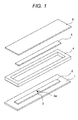
- Fig. 1 is an exploded view of a radio frequency IC tag according to a first embodiment of the present invention.
- Fig. 2 is a sectional view of the radio frequency IC tag assembled in Fig. 1 as viewed in its transverse direction.
- a copper foil-made first antenna 2 given tin plating or the like is formed on an upper surface of a plate-shaped first spacer 1 made up of a synthetic resin such as a polyimide resin material or the like.
- An IC chip 3 with information recorded thereon is mounted on an upper surface of the first antenna 2.
- a slit 3a for impedance matching and prevention of electrostatic breakdown of the IC chip is formed at a part where the IC chip 3 is mounted on the first antenna 2.
- a copper foil-made second antenna 5 given the same tin plating or the like is formed on a lower surface of a top cover 6.
- a second spacer 4 is shaped in a hollow form having a predetermined thickness.
- the top cover 6 and the first spacer 1 are provided on both sides of the second spacer 4 in a state in which the first antenna 2 and the second antenna 5 are opposed to each other on both sides thereof.
- the top cover 6, the first spacer 1 and the second spacer 4 constitute the case which accommodates the IC chip 3 and the first and second antennas 2 and 5 therein.
- the thickness of the second spacer 4 defines space between the first antenna 2 and the second antenna 5.
- the first antenna 2 and the second antenna 5 can also be formed by being metallized or metal-deposited directly on the first spacer 1 and the top cover 6 respectively.
- the radio frequency IC tag is formed by assembling the respective members in this way.
- Fig. 2 is a view showing a sectional configuration of the radio frequency IC tag as viewed in its transverse direction.
- the first antenna 2 which radiates the information of the IC chip 3 through the use of a weak radio wave
- the second antenna 5 which performs an amplifying operation in resonance with the weak radio wave of the first antenna 2
- a hollow portion 7 of the second spacer 4 as a dielectric.
- the radio frequency IC tag is mounted with the first spacer 1 side as a body for an object, then management or control of the object can be carried out since the information of the IC chip 3 is read by receiving the radio wave radiated from the second antenna 5. Since the first spacer 1 keeps the first antenna 2 away from the object at a predetermined distance in a state in which the radio frequency IC tag is being mounted to the object, the radio wave can be radiated even if the object is a metal or one containing moisture.
- the radio frequency IC tag according to the present embodiment can be used with being mounted to a wafer or a metal or the like even in a semiconductor manufacturing process which needs chemical resistance, dustproofness and an antistatic or static-controlled property.
- the thickness of the second spacer 4 i.e., the thickness T of the hollow portion 7 from 0.3mm or over to 5mm or under.
- the thickness T may most preferably be 1mm or so.
- the thickness of the first spacer 1 and the thickness of the top cover 6 are respectively set so as to range from about 0.1mm to about 2mm. No particular restrictions are imposed on the dimensions or sizes in the transverse and longitudinal directions, of the first spacer 1, second spacer 4 and top cover 6. The dimensions thereof may appropriately be determined depending upon dimensions easy to manufacture them and each object to which the radio frequency IC tag is mounted.
- first antenna 2 and the second antenna 5 are formed of copper foil, they are not limited to it. They may also be formed of aluminum foil, conductive ink (one obtained by kneading ink with a carbon resin) or the like.
- the thicknesses of the first antenna 2 and the second antenna 5 are set to, for example, about 0.02mm and the lengths thereof are set to 53mm due to the reason to be described later. Incidentally, no particular restriction is imposed on the width of the second antenna 5.
- the radio frequency IC tag of the present invention is configured in such a manner that the first antenna 2 equipped with the IC chip 3 and the second antenna 5 for amplifying the radio wave radiated from the first antenna 2 are placed in opposing relationship in the case constituted of the first spacer 1, the second spacer 4 and the top cover 6, and the hollow portion 7 existing between the first antenna 2 and the second antenna 5 is brought into the vacuum state or airspace or filled with the inert gas such as nitrogen, argon or the like to form the dielectric layer of desired permittivity.
- the dielectric layer of desired permittivity can also be formed by charging the hollow portion 7 with a synthetic resin or synthetic resin form instead of air or the like. Incidentally, when the hollow portion 7 is filled with the gas or synthetic resin, the strength of the entire radio frequency IC tag can be increased.
- high-strength resins such as ABS, AES, AS, PC, POM and the like are used.
- ABS is a hard and high strength resin which is strong in impact and has strong resistance to an acid, a base, salt water, alcohol and the like.
- PC polycarbonate
- POM polyoxymethylene
- ABS is a hard and high strength resin which is strong in impact and has strong resistance to an acid, a base, salt water, alcohol and the like.
- PC polycarbonate
- POM polyoxymethylene
- a POM resin polyoxymethlene, polyacetal or the like
- POM resin is engineering plastic excellent in terms of mechanical characteristics such as a breaking strength or the like, and wear resistance characteristics or the like.
- Homopolymer and copolymer are known as the POM resin.
- the POM resin may preferably be used properly according to mounting uses or the like for the radio frequency IC tag. Since the most striking characteristic of the POM resin is self-lubricative, it has characteristics useful in the use for parts always subjected to friction as in gear wheels, bearings and the like.
- the POM resin may preferably be used for the radio frequency IC tag applied to such uses that the characteristics can be utilized effectively. Further, since the POM resin is also high in crystallinity, it exhibits characteristics satisfactory in strength and heat resistance too. Incidentally, caution is required since it causes thermal decomposition when it stays in a cylinder for long hours upon injection molding.
- antistatic polypropylene As the material for the first spacer 1, the second spacer 4, and the top cover 6,antistatic polypropylene, antistatic ABS obtained by adding conductive high polymer or the like to the normal ABS resin, a resin used in a manufacturing process line of semiconductor materials such as silicon, and the like are used. That is, although the static-controlled materials each having the antistatic effect are used as the material for the second spacer 4, these static-controlled materials can be allowed to have the antistatic effect by being added with the conductive high polymer upon polymerization of a high-purity ABS resin. By using a material for a wafer carrier used in a semiconductor manufacturing line, an antistatic effect corresponding to low dust generation can be obtained.
- a fluorocarbon resin can be used to enhance chemical resistance.
- the fluorocarbon resin having the chemical resistance for example, PFA (Pefluoroalkoxy: Perfluoroalkilvinylether copolymer resin) has high chemical resistance and solvent resistance.
- materials other than the fluorocarbon resin such as PP (Polypropylene), PEEK (Polyetheretherketone), PPS (PolyPhenilen Sulfid), etc. can also be used.
- PP Polypropylene
- PEEK Polyetheretherketone
- PPS PolyPhenilen Sulfid
- PP is excellent in bending characteristic and shock resistance and has chemical resistance excellent in strong inorganic acid, base, and alcohol and the like.
- PEEK exhibits chemical resistance high both inorganically and organically. Further, PPS has a heat resistance of 200°C and is extremely satisfactory in dimensional stability. PPS is excellent in acid resistance and alkali resistance and resistant to organic solvents, and is excellent even in chemical resistance.
- PPS PolyPhenilen Sulfid
- the chemical resistance material is super engineering plastic which endures up to the neighborhood of 260°C corresponding to a deflection temperature under load.
- PPS there are known cross-linked, semicross-linked and straight-chain types. Since the deflection temperature under load thereof is higher than a melting-point temperature of solder, PPS is preferably used in surface-mount electronic parts for reflow solder.
- PPS is good in fluidity, burrs are apt to occur upon injection molding. Since it is necessary to raise a molding temperature at the molding of PPS from 130°C to 150°C, a mold therefor needs an oil-based temperature adjustment and heat retention by a cartridge heater.
- the relationship between the length of the second antenna 5 and its communication distance will next be explained.
- the first antenna 2 propagates the information of the IC chip 3 to the second antenna 5 by a weak radio wave.
- the second antenna 5 exhibits amplifying action in resonance with the frequency of the radio wave radiated from the first antenna 2.
- the amplified radio wave is radiated from the second antenna 5 to the outside and hence the radio wave strong in radio field intensity is radiated to make it possible to keep the communication distance long. Since a resonant point changes according to the length of the second antenna 5 at this time, the length of the second antenna 5 becomes an important factor for increasing the communication distance. It is of course needless to say that the length of the resonating second antenna 5 differs according to the permittivity of a dielectric charged into the hollow portion 7.
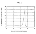
- Fig. 3 is a characteristic diagram showing an experimental result in which communication distances relative to the length of the second antenna where the permittivity of the dielectric interposed between the first antenna and the second antenna is held constant, have been measured, in the radio frequency IC tag in Fig. 2.
- the communication distance is kept constant as about 12mm as shown in Fig. 3 until the length of the second antenna 5 is at about 45mm, the communication distance suddenly increases from the length exceeding 45mmwhen the length of the second antenna 5 is increased.
- the second antenna 5 is set to a length of 53mm, the communication distance reaches about 130mm at maximum. That is, the point where the length of the second antenna 5 reaches 53mm becomes the resonant point relative to the radiated radio wave of the first antenna 2.
- the radio frequency IC tag is brought into a state unable to entirely communicate (communication distance: 0).
- 53mm at which the communication distance becomes the longest was set to the length of the second antenna 5 on the basis of the experimental result.
- the length of the second antenna 5 when the length of the second antenna 5 is set to 1/2 (i.e., ⁇ /2) of the wavelength of a radio wave of a predetermined frequency (2.45GHz) used to read the information from the radio frequency IC tag, the communication distance becomes the longest. However, the length thereof changes according to the permittivity of a substance charged between the first antenna 2 and the second antenna 5, and the like. When an insulating material large in permittivity is used as the charged substance, the length of the second antenna 5 can be shortened. It is known that when, for example, chloroburane rubber is used as the charged insulating material although an experimental result is not shown in the drawing, the length of the second antenna 5 can be shortened from 53mm referred to above to 45mm.
- the radio frequency IC tag can be realized which is capable of combining both thinning thereof owing to the addition of the second spacer 4 and the second antenna 5 and shortening of the dimensions in the longitudinal direction due to the shortening of the second antenna 5 by selecting the insulating material of suitable permittivity and filling the hollow portion 7 with it, and of ensuring a relatively long communication distance. Since the length of the first antenna 2 can also be set to the same length of 45mm as that of the second antenna 5 in the above example, the dimensions in the longitudinal direction can be shortened along with the thinning. Consequentially, miniaturization of the radio frequency IC tag can be realized.
- the permittivity between the first antenna 2 and the second antenna 5 can arbitrarily be changed by bringing the hollow portion 7 to vacuum, filling the hollow portion 7 with air or inert gas or interposing the resin into the hollow portion 7 to form the dielectric. Changing the permittivity in this way makes it possible to arbitrarily change radio wave propagation efficiency between the first antenna 2 and the second antenna 5. Consequentially, the strength of the radio wave radiated from the second antenna 5 can arbitrarily be changed.
- the permittivity is approximately "1". Since, however, the permittivity ranges from “2 to 4" if the synthetic resin foam is interposed therein, the communication distance can be made long even though the thickness T of the second spacer 4 is made thin. Since the permittivity can selectively be changed even in the case of the same material by changing a foam rate of the synthetic resin foam, the communication distance can be controlled by changing the foam rate. That is, when the synthetic resin foam is provided as the dielectric, its permittivity results in permittivity of its synthetic resin itself where the foam rate is "0%”. As the foam rate approaches "100%", its permittivity can be made close to air' s permittivity "1".
- FIGs. 4A and 4B are perspective views of the radio frequency IC tag according to the second embodiment of the present invention, wherein Fig. 4A shows a shape having mounting openings, and Fig. 4B shows a shape having mounting grooves, respectively.
- the first spacer 1 and the top cover 6 are formed in the same size in the first embodiment, whereas a first spacer 12 is made longer than a top cover 16 as viewed in a longitudinal direction in the second embodiment.
- ends 13 are formed on both sides.
- the mounting openings 14 are defined in the ends 13 respectively.
- the radio frequency IC tag 11 Since the radio frequency IC tag 11 has durability, weatherability, dustproofness and waterproofness and is given antistatic measures, it is possible to mount the radio frequency IC tag to a container, a cylinder and a power apparatus or the like exposed to the outdoors and control or manage information about those mounted objects.
- ends 23 can be formed on both sides by making a first spacer 22 longer than a top cover 26 as viewed in a longitudinal direction in a manner similar to Fig. 4A. Forming the mounting grooves 24 at the ends 23 makes it possible to easily mount the radio frequency IC tag 21 to an object to be mounted. Since the present radio frequency IC tag 21 has durability, weatherability, dustproofness and waterproofness and is given antistatic measures, it is possible to mount a waste management apparatus exposed to the outdoors and a semiconductor material or the like manufactured in a clean room, manage information about those obj ects to be mounted and thereby carry out process control.
- the radio frequency IC tag according to the present invention has waterproofness, weatherability and resistance to dust and is brought to a rugged structure, it is possible to mount it to a transporter and an outdoor power apparatus or the like and perform their operational management or the like. Since the radio frequency IC tag according to the present invention is provided with the antistatic property hard to take the electrical charge, manufacturing management high in production yield can be carried out by using the radio frequency IC tag in a semiconductor manufacturing apparatus or the like.
Landscapes
- Engineering & Computer Science (AREA)
- Physics & Mathematics (AREA)
- General Physics & Mathematics (AREA)
- Theoretical Computer Science (AREA)
- Electromagnetism (AREA)
- Microelectronics & Electronic Packaging (AREA)
- Computer Hardware Design (AREA)
- Computer Networks & Wireless Communication (AREA)
- Toxicology (AREA)
- Health & Medical Sciences (AREA)
- Computer Vision & Pattern Recognition (AREA)
- Artificial Intelligence (AREA)
- General Health & Medical Sciences (AREA)
- Details Of Aerials (AREA)
Abstract
Description
- The present invention relates to a radio frequency IC tag comprising an IC chip with information recorded thereon and an antenna for radio transmitting the information recorded on the IC chip by radio waves, and particularly to a radio frequency IC tag improved in durability and weatherability and a method for manufacturing the radio frequency IC tag.
- In recent years, radio frequency IC tags have been widely used in information management and physical distribution management or the like of articles. Further, these radio frequency IC tags are beginning to be used even when animals and the like are specified and managed. Each of such radio frequency IC tags comprises a small IC chip with information recorded thereon and a small antenna which transmits the information of the IC chip by radio. Such a radio frequency IC tag has, for example, a small IC chip having dimensions: about 0.4mm (width) x 0.4mm (depth) x 0.1mm (height), which is mounted to the neighborhood of a central portion of a slender antenna, and is used with being attached to each of articles, animals and the like. Thus, information (i.e., information about the attributes or the like of individual articles and animals) recorded on the IC chip can be read on a noncontact basis by holding a read writer over the corresponding radio frequency IC tag.
- In order to attach such radio frequency IC tags on the articles and animals or the like, the radio frequency IC tags may preferably be set as small as possible and be light in weight. Further, a communication distance may preferably be set as long as possible. To this end, there is a need to reduce the antenna of each radio frequency IC tag and make its directivity satisfactory. When the radio frequency IC tags are mounted to articles and livestock or the like exposed to the outdoors, they need to be excellent in durability, weatherability, dustproofness, moistureproofness and the like. A technique of a radio frequency IC tag wherein an antenna section is accommodated in a dielectric case to realize such an objective, has been disclosed (for example,
Japanese Patent Laid-Open No. 2003-298464 - Since, however, the radio frequency IC tag of the
patent document 1 referred to above makes use of a general synthetic resin foam as a dielectric case, a moisture-proof effect might be impaired due tomoisture-absorbent action, and the dielectric case might be deformed or cracked due to ultraviolet rays and raindrops or the like. That is, there may be cases in which weatherability, dustproofness, waterproofness and the like are impaired due to deterioration of the synthetic resin foam over time. Further, when the radio frequency IC tag is used in a clean room or the like at a semiconductor manufacturing site, the degree of cleanness might be degraded due to dust generation or the like from the synthetic resin foam, and semiconductor products might be subjected to electrostatic breakdown due to an electrostatic charge phenomenon of the synthetic resin foam. Consequentially, there is a fear that the production yields of the semiconductor products are reduced. Incidentally, since one of such a type that the antenna section is covered with the conventional radio frequency IC tag of such a type as described in thepatent document 1 takes such a configuration that it is nipped by a general resin case, as well as the radio frequency IC tag of thepatent document 1, it does not take sufficient measures against weatherability, dustproofness, waterproofness and electrostatic prevention or the like. - Since the radio frequency IC tag of the
patent document 1 takes the configuration using the microstrip antenna, the radio wave of the IC chip is efficiently radiated from the radiation conductive layer (antenna layer) side without being radiated to the earth conductive layer (ground layer). Therefore, the directivity of the antenna is relatively satisfactory. Since, however, the areas of the radiation conductive layer (antenna layer) and the earth conductive layer (ground layer) must be increased to further strengthen the strength of the radio wave radiated from the microstrip antenna, the radio frequency IC tag will eventually increase in size. - The present invention has been made in view of the above problems. It is therefore an object of the present invention to provide a radio frequency IC tag which is excellent in weatherability, dustproofness, waterproofness, static protection and the like and capable of making a communication distance long even though an antenna section is made small in configuration, and a method for manufacturing the same.
- A radio frequency IC tag of the present invention has been created in the light of the above object. A first antenna to which an IC chip is mounted, and a second antenna which amplifies a radio wave radiated from the first antenna, are disposed on their corresponding opposite surfaces inside a case. A hollow portion defined between the first antenna and the second antenna is brought into a vacuum state or filled with air, inert gas, a synthetic resin or synthetic resin foam to form a dielectric layer. As a material for the case, high-strength resins such as ABS (Acrylonitrite-Butadiene-Styrene resin), AES (Acrylonitrile-Ethylene-Styrene), AS (Acrylonitrile-Styrene copolymer), PC (PolyCarbonate), POM (PolyOxyMethylene), etc. are used. Alternatively, antistatic polypropylene, antistatic ABS formed by adding conductive high polymer or the like to an ABS resin, a resin used in a semiconductor manufacturing process line, etc. are used. As an alternative to above, a fluorocarbon resin high in chemical resistance is used. Mounting openings are provided at case ends or mounting grooves are provided thereat to configure a structure easy to mount the radio frequency IC tag to an object to be attached.
- According to the present invention, the first antenna and the second antenna are configured so as to be accommodated within the case inclusive of the CI chip to thereby enhance durability and weatherability against the environment. Using electrostatically-uncharged static-controlled material as a material for forming the case makes it possible to reduce an electrostatic charge phenomenon to the radio frequency IC tag and prevent dust generation due to deterioration with time. Further, since the second antenna for amplifying the radiated radio wave of the first antenna is provided, the radio wave radiated from the radio frequency IC tag becomes strong, so that a communication distance from the radio frequency IC tag can be made long.
-
- Fig. 1 is an exploded view of a radio frequency IC tag showing a first embodiment according to the present invention;
- Fig. 2 is a sectional view of the radio frequency IC tag assembled in Fig. 1 as viewed in its transverse direction;
- Fig. 3 is a characteristic diagram showing an experimental result in which communication distances relative to the length of a second antenna where the permittivity of a dielectric interposed between a first antenna and the second antenna is held constant have been measured, in the radio frequency IC tag in Fig. 2; and
- Figs. 4A and 4B are perspective views showing a radio frequency IC tag according to a second embodiment of the present invention, wherein Fig. 4A shows a shape having mounting openings and Fig. 4B shows a shape having mounting grooves.
- A radio frequency IC tag according to the mode (hereinafter called "embodiment") for implementing the present invention will hereinafter explained with reference to the accompanying drawings by citing preferred examples.
- In the radio frequency IC tag according to the present invention, a first antenna equipped with an IC chip is disposed with respect to an inner surface on the bottom side, of a case made of a synthetic resin, and a second antenna that resonates with a radiated radio wave of the first antenna is disposed with respect to an inner surface on the cover side, of the case. Incidentally, a high-strength material excellent in impact resistance, a chemical-resistance material excellent in chemical resistance, an antistatic or static-controlled material free of the occurrence of static electricity and the like are selected and used for the case. A hollow portion in the case is brought to a vacuum state or filled with air, an inert gas, synthetic resin foam or the like to form a dielectric layer. With such a configuration, the strength of the radiated radio wave becomes strong by virtue of an amplifying effect produced by the second antenna and hence a communication distance gets long. Further, the IC chip, the antennas and the like are accommodated into the case to make it possible to enhance durability, weatherability, dustproofness and waterproofness. Since the synthetic resin of the case makes use of the static-controlled material,an electrostatic charge phenomenon can also be prevented from occurring.
- Fig. 1 is an exploded view of a radio frequency IC tag according to a first embodiment of the present invention. Fig. 2 is a sectional view of the radio frequency IC tag assembled in Fig. 1 as viewed in its transverse direction. As shown in Fig. 1, a copper foil-made
first antenna 2 given tin plating or the like is formed on an upper surface of a plate-shapedfirst spacer 1 made up of a synthetic resin such as a polyimide resin material or the like. AnIC chip 3 with information recorded thereon is mounted on an upper surface of thefirst antenna 2. Aslit 3a for impedance matching and prevention of electrostatic breakdown of the IC chip is formed at a part where theIC chip 3 is mounted on thefirst antenna 2. - A copper foil-made
second antenna 5 given the same tin plating or the like is formed on a lower surface of atop cover 6. Asecond spacer 4 is shaped in a hollow form having a predetermined thickness. Thetop cover 6 and thefirst spacer 1 are provided on both sides of thesecond spacer 4 in a state in which thefirst antenna 2 and thesecond antenna 5 are opposed to each other on both sides thereof. Thus, thetop cover 6, thefirst spacer 1 and thesecond spacer 4 constitute the case which accommodates theIC chip 3 and the first andsecond antennas second spacer 4 defines space between thefirst antenna 2 and thesecond antenna 5. Incidentally, thefirst antenna 2 and thesecond antenna 5 can also be formed by being metallized or metal-deposited directly on thefirst spacer 1 and thetop cover 6 respectively. - The radio frequency IC tag is formed by assembling the respective members in this way. Fig. 2 is a view showing a sectional configuration of the radio frequency IC tag as viewed in its transverse direction. As shown in Fig. 2, the
first antenna 2 which radiates the information of theIC chip 3 through the use of a weak radio wave, and thesecond antenna 5 which performs an amplifying operation in resonance with the weak radio wave of thefirst antenna 2, are disposed in opposing relationship with ahollow portion 7 of thesecond spacer 4 as a dielectric. Thus, if the radio frequency IC tag is mounted with thefirst spacer 1 side as a body for an object, then management or control of the object can be carried out since the information of theIC chip 3 is read by receiving the radio wave radiated from thesecond antenna 5. Since thefirst spacer 1 keeps thefirst antenna 2 away from the object at a predetermined distance in a state in which the radio frequency IC tag is being mounted to the object, the radio wave can be radiated even if the object is a metal or one containing moisture. Thus, the radio frequency IC tag according to the present embodiment can be used with being mounted to a wafer or a metal or the like even in a semiconductor manufacturing process which needs chemical resistance, dustproofness and an antistatic or static-controlled property. - In order to effectively propagate the weak radio wave radiated from the
first antenna 2 to thesecond antenna 5, there is a need to suppress the thickness of thesecond spacer 4, i.e., the thickness T of thehollow portion 7 from 0.3mm or over to 5mm or under. When thehollow portion 7 is air (that is, when air becomes a dielectric), the thickness T may most preferably be 1mm or so. Incidentally, the thickness of thefirst spacer 1 and the thickness of thetop cover 6 are respectively set so as to range from about 0.1mm to about 2mm. No particular restrictions are imposed on the dimensions or sizes in the transverse and longitudinal directions, of thefirst spacer 1,second spacer 4 andtop cover 6. The dimensions thereof may appropriately be determined depending upon dimensions easy to manufacture them and each object to which the radio frequency IC tag is mounted. - Although the
first antenna 2 and thesecond antenna 5 are formed of copper foil, they are not limited to it. They may also be formed of aluminum foil, conductive ink (one obtained by kneading ink with a carbon resin) or the like. The thicknesses of thefirst antenna 2 and thesecond antenna 5 are set to, for example, about 0.02mm and the lengths thereof are set to 53mm due to the reason to be described later. Incidentally, no particular restriction is imposed on the width of thesecond antenna 5. - That is, the radio frequency IC tag of the present invention is configured in such a manner that the
first antenna 2 equipped with theIC chip 3 and thesecond antenna 5 for amplifying the radio wave radiated from thefirst antenna 2 are placed in opposing relationship in the case constituted of thefirst spacer 1, thesecond spacer 4 and thetop cover 6, and thehollow portion 7 existing between thefirst antenna 2 and thesecond antenna 5 is brought into the vacuum state or airspace or filled with the inert gas such as nitrogen, argon or the like to form the dielectric layer of desired permittivity. The dielectric layer of desired permittivity can also be formed by charging thehollow portion 7 with a synthetic resin or synthetic resin form instead of air or the like. Incidentally, when thehollow portion 7 is filled with the gas or synthetic resin, the strength of the entire radio frequency IC tag can be increased. - As the material for the
first spacer 1, thesecond spacer 4, and thetop cover 6, high-strength resins such as ABS, AES, AS, PC, POM and the like are used. - Of these high-strength resins, ABS is a hard and high strength resin which is strong in impact and has strong resistance to an acid, a base, salt water, alcohol and the like. PC (polycarbonate) is excellent in impact resistance and excellent in terms of resistance to a weak acid, a base, oil, alcohol and the like at room temperatures. Further, POM (polyoxymethylene) is an engineering plastic material excellent in terms of strength, elastic modulus, impact resistance and the like.
- In particular, a POM resin (polyoxymethlene, polyacetal or the like) is engineering plastic excellent in terms of mechanical characteristics such as a breaking strength or the like, and wear resistance characteristics or the like. Homopolymer and copolymer are known as the POM resin. Since there are differences in strength, heat resistance, molding conditions and the like between the homopolyer and the copolymer, the POM resin may preferably be used properly according to mounting uses or the like for the radio frequency IC tag. Since the most striking characteristic of the POM resin is self-lubricative, it has characteristics useful in the use for parts always subjected to friction as in gear wheels, bearings and the like. Therefore, the POM resin may preferably be used for the radio frequency IC tag applied to such uses that the characteristics can be utilized effectively. Further, since the POM resin is also high in crystallinity, it exhibits characteristics satisfactory in strength and heat resistance too. Incidentally, caution is required since it causes thermal decomposition when it stays in a cylinder for long hours upon injection molding.
- As the material for the
first spacer 1, thesecond spacer 4, and thetop cover 6,antistatic polypropylene, antistatic ABS obtained by adding conductive high polymer or the like to the normal ABS resin, a resin used in a manufacturing process line of semiconductor materials such as silicon, and the like are used. That is, although the static-controlled materials each having the antistatic effect are used as the material for thesecond spacer 4, these static-controlled materials can be allowed to have the antistatic effect by being added with the conductive high polymer upon polymerization of a high-purity ABS resin. By using a material for a wafer carrier used in a semiconductor manufacturing line, an antistatic effect corresponding to low dust generation can be obtained. - As the material for the
first spacer 1, thesecond spacer 4, and thetop cover 6, a fluorocarbon resin can be used to enhance chemical resistance. As the fluorocarbon resin having the chemical resistance, for example, PFA (Pefluoroalkoxy: Perfluoroalkilvinylether copolymer resin) has high chemical resistance and solvent resistance. In order to cause it to have chemical resistance, materials other than the fluorocarbon resin, such as PP (Polypropylene), PEEK (Polyetheretherketone), PPS (PolyPhenilen Sulfid), etc. can also be used. PP is excellent in bending characteristic and shock resistance and has chemical resistance excellent in strong inorganic acid, base, and alcohol and the like. PEEK exhibits chemical resistance high both inorganically and organically. Further, PPS has a heat resistance of 200°C and is extremely satisfactory in dimensional stability. PPS is excellent in acid resistance and alkali resistance and resistant to organic solvents, and is excellent even in chemical resistance. - In particular, PPS (PolyPhenilen Sulfid) used as the chemical resistance material is super engineering plastic which endures up to the neighborhood of 260°C corresponding to a deflection temperature under load. As such PPS, there are known cross-linked, semicross-linked and straight-chain types. Since the deflection temperature under load thereof is higher than a melting-point temperature of solder, PPS is preferably used in surface-mount electronic parts for reflow solder. Thus, it is desirable to use PPS in the radio frequency IC tag applied to such uses that such characteristics can be utilized effectively. Incidentally, since PPS is good in fluidity, burrs are apt to occur upon injection molding. Since it is necessary to raise a molding temperature at the molding of PPS from 130°C to 150°C, a mold therefor needs an oil-based temperature adjustment and heat retention by a cartridge heater.
- The relationship between the length of the
second antenna 5 and its communication distance will next be explained. Thefirst antenna 2 propagates the information of theIC chip 3 to thesecond antenna 5 by a weak radio wave. In doing so, thesecond antenna 5 exhibits amplifying action in resonance with the frequency of the radio wave radiated from thefirst antenna 2. As a result, the amplified radio wave is radiated from thesecond antenna 5 to the outside and hence the radio wave strong in radio field intensity is radiated to make it possible to keep the communication distance long. Since a resonant point changes according to the length of thesecond antenna 5 at this time, the length of thesecond antenna 5 becomes an important factor for increasing the communication distance. It is of course needless to say that the length of the resonatingsecond antenna 5 differs according to the permittivity of a dielectric charged into thehollow portion 7. - Fig. 3 is a characteristic diagram showing an experimental result in which communication distances relative to the length of the second antenna where the permittivity of the dielectric interposed between the first antenna and the second antenna is held constant, have been measured, in the radio frequency IC tag in Fig. 2. Although the communication distance is kept constant as about 12mm as shown in Fig. 3 until the length of the
second antenna 5 is at about 45mm, the communication distance suddenly increases from the length exceeding 45mmwhen the length of thesecond antenna 5 is increased. When thesecond antenna 5 is set to a length of 53mm, the communication distance reaches about 130mm at maximum. That is, the point where the length of thesecond antenna 5 reaches 53mm becomes the resonant point relative to the radiated radio wave of thefirst antenna 2. When the length of thesecond antenna 5 is further increased, the communication distance suddenly becomes short in reverse. When a length of about 60mm is reached, the radio frequency IC tag is brought into a state unable to entirely communicate (communication distance: 0). In the first embodiment, 53mm at which the communication distance becomes the longest, was set to the length of thesecond antenna 5 on the basis of the experimental result. - It is theoretically known that when the length of the
second antenna 5 is set to 1/2 (i.e., λ/2) of the wavelength of a radio wave of a predetermined frequency (2.45GHz) used to read the information from the radio frequency IC tag, the communication distance becomes the longest. However, the length thereof changes according to the permittivity of a substance charged between thefirst antenna 2 and thesecond antenna 5, and the like. When an insulating material large in permittivity is used as the charged substance, the length of thesecond antenna 5 can be shortened. It is known that when, for example, chloroburane rubber is used as the charged insulating material although an experimental result is not shown in the drawing, the length of thesecond antenna 5 can be shortened from 53mm referred to above to 45mm. - Thus, the communication distance and the length of the
second antenna 5, and the permittivity of the insulatingmaterial charged between thefirst antenna 2 and thesecond antenna 5 are placed in a trade-off relationship. Therefore, the radio frequency IC tag can be realized which is capable of combining both thinning thereof owing to the addition of thesecond spacer 4 and thesecond antenna 5 and shortening of the dimensions in the longitudinal direction due to the shortening of thesecond antenna 5 by selecting the insulating material of suitable permittivity and filling thehollow portion 7 with it, and of ensuring a relatively long communication distance. Since the length of thefirst antenna 2 can also be set to the same length of 45mm as that of thesecond antenna 5 in the above example, the dimensions in the longitudinal direction can be shortened along with the thinning. Consequentially, miniaturization of the radio frequency IC tag can be realized. - Using the high-strength material, chemical resistant material and static-controlled material for the
first spacer 1,second spacer 4 andtop cover 6 constituting the case of the radio frequency IC tag as described above makes it possible to enhance durability, weatherability, dustproofness and waterproofness and prevent the electrostatic charge phenomenon. Further, the permittivity between thefirst antenna 2 and thesecond antenna 5 can arbitrarily be changed by bringing thehollow portion 7 to vacuum, filling thehollow portion 7 with air or inert gas or interposing the resin into thehollow portion 7 to form the dielectric. Changing the permittivity in this way makes it possible to arbitrarily change radio wave propagation efficiency between thefirst antenna 2 and thesecond antenna 5. Consequentially, the strength of the radio wave radiated from thesecond antenna 5 can arbitrarily be changed. - When the dielectric interposed in the
hollow portion 7 of thesecond spacer 4 is of vacuum or air, for example, the permittivity is approximately "1". Since, however, the permittivity ranges from "2 to 4" if the synthetic resin foam is interposed therein, the communication distance can be made long even though the thickness T of thesecond spacer 4 is made thin. Since the permittivity can selectively be changed even in the case of the same material by changing a foam rate of the synthetic resin foam, the communication distance can be controlled by changing the foam rate. That is, when the synthetic resin foam is provided as the dielectric, its permittivity results in permittivity of its synthetic resin itself where the foam rate is "0%". As the foam rate approaches "100%", its permittivity can be made close to air' s permittivity "1". - A second embodiment of the present invention will explain a mounting structure of a radio frequency IC tag. Figs. 4A and 4B are perspective views of the radio frequency IC tag according to the second embodiment of the present invention, wherein Fig. 4A shows a shape having mounting openings, and Fig. 4B shows a shape having mounting grooves, respectively. The
first spacer 1 and thetop cover 6 are formed in the same size in the first embodiment, whereas afirst spacer 12 is made longer than atop cover 16 as viewed in a longitudinal direction in the second embodiment. Thus, when asecond spacer 15 and thetop cover 16 are disposed on thefirst spacer 12 as shown in Fig. 4A, ends 13 are formed on both sides. The mountingopenings 14 are defined in theends 13 respectively. It is thus possible to easily mount the radiofrequency IC tag 11 onto an object to be mounted. Since the radiofrequency IC tag 11 has durability, weatherability, dustproofness and waterproofness and is given antistatic measures, it is possible to mount the radio frequency IC tag to a container, a cylinder and a power apparatus or the like exposed to the outdoors and control or manage information about those mounted objects. - As shown in Fig. 4B, ends 23 can be formed on both sides by making a
first spacer 22 longer than atop cover 26 as viewed in a longitudinal direction in a manner similar to Fig. 4A. Forming the mountinggrooves 24 at theends 23 makes it possible to easily mount the radiofrequency IC tag 21 to an object to be mounted. Since the present radiofrequency IC tag 21 has durability, weatherability, dustproofness and waterproofness and is given antistatic measures, it is possible to mount a waste management apparatus exposed to the outdoors and a semiconductor material or the like manufactured in a clean room, manage information about those obj ects to be mounted and thereby carry out process control. - In general, charged electrical charges are hard to scatter because a synthetic resin such as plastic is high in electrical insulating property. Therefore, there is a fear that dust is adhered to a synthetic resin product to cause its depreciation, instruments and an IC chip are caused to malfunction due to the electrical charges and a semiconductor product is subjected to an electrostatic breakdown. Since, however, the radio frequency IC tag according to the present invention has waterproofness, weatherability and resistance to dust and is brought to a rugged structure, it is possible to mount it to a transporter and an outdoor power apparatus or the like and perform their operational management or the like. Since the radio frequency IC tag according to the present invention is provided with the antistatic property hard to take the electrical charge, manufacturing management high in production yield can be carried out by using the radio frequency IC tag in a semiconductor manufacturing apparatus or the like.
Claims (13)
- A radio frequency IC tag which transmits information recorded on an IC chip by radio, comprising:a first antenna which is equipped with the IC chip and transmits the information recorded on the IC chip by radio waves;a second antenna which resonates with a radio wave radiated from the first antenna and radiates the amplified radio wave to transmit the information recorded on the IC chip by radio; anda hollow case,wherein the first antenna and the second antenna are respectively placed in opposite positions inside the case.
- The radio frequency IC tag according to claim 1,
wherein the case is placed in a vacuum state thereinside. - The radio frequency IC tag according to claim 1,
wherein the case is internally filled with air or an inert gas. - The radio frequency IC tag according to claim 1,
wherein a synthetic resin foam is charged between the first antenna and the second antenna in the case. - The radio frequency IC tag according to claim 4,
wherein desired permittivity is obtained by changing a foam rate of the synthetic resin foam. - The radio frequency IC tag according to claim 1,
wherein a material for the case is any of ABS, AES, AS, PC and POM or a high-strength resin having performance equivalent to them. - The radio frequency IC tag according to claim 5,
wherein a material for the case is any of antistatic polypropylene, antistatic ABS obtained by adding conductive high polymer to an ABS resin and a resin used in a semiconductor manufacturing process line. - The radio frequency IC tag according to claim 5,
wherein a material for the case is a fluorocarbon resin. - The radio frequency IC tag according to claim 8,
wherein a material for the case is any of PP, PEEK, PFA and PPS. - The radio frequency IC tag according to claim 9,
wherein mounting openings are respectively provided at ends of the case. - The radio frequency IC tag according to claim 9,
wherein mounting grooves are respectively provided at ends of the case. - A method for manufacturing a radio frequency IC tag that transmits information recorded on an IC chip by radio, comprising the steps of:allowing a first spacer, a second spacer and a top cover to constitute a case;forming a first antenna in one surface of the synthetic resin-made first spacer;mounting the IC chip in the first antenna;disposing the second spacer with its hollow cube as an outer shell, on the first spacer on the side of a surface thereof on which the first antenna is formed;forming a second antenna for amplifying a radio wave in resonance with a radio wave radiated from the first antenna, on one surface of the top cover; anddisposing the top cover on the second spacer in such a manner that the second antenna is opposite to the first antenna.
- The method according to claim 12,
wherein any of air, an inert gas and a synthetic resin foam is charged into the case, and the second spacer makes use of a high-strength resin, a chemical resistant resin and a static-controlled resin having an antistatic effect.
Applications Claiming Priority (1)
| Application Number | Priority Date | Filing Date | Title |
|---|---|---|---|
| JP2005132771A JP4778264B2 (en) | 2005-04-28 | 2005-04-28 | Wireless IC tag and method of manufacturing wireless IC tag |
Publications (2)
| Publication Number | Publication Date |
|---|---|
| EP1717731A1 true EP1717731A1 (en) | 2006-11-02 |
| EP1717731B1 EP1717731B1 (en) | 2009-11-11 |
Family
ID=36601143
Family Applications (1)
| Application Number | Title | Priority Date | Filing Date |
|---|---|---|---|
| EP05257749A Ceased EP1717731B1 (en) | 2005-04-28 | 2005-12-16 | Radio frequency IC tag and method for manufacturing same |
Country Status (4)
| Country | Link |
|---|---|
| US (1) | US7535365B2 (en) |
| EP (1) | EP1717731B1 (en) |
| JP (1) | JP4778264B2 (en) |
| NO (1) | NO20055985L (en) |
Cited By (2)
| Publication number | Priority date | Publication date | Assignee | Title |
|---|---|---|---|---|
| EP1969536A1 (en) * | 2006-01-06 | 2008-09-17 | Sdu Identification B.V. | Identity document having a chip |
| EP3287956A4 (en) * | 2015-04-22 | 2019-03-13 | Toyo Seikan Group Holdings, Ltd. | RF LABEL |
Families Citing this family (26)
| Publication number | Priority date | Publication date | Assignee | Title |
|---|---|---|---|---|
| CA2613241A1 (en) | 2005-06-21 | 2007-01-04 | Cardiomems, Inc. | Method of manufacturing implantable wireless sensor for in vivo pressure measurement |
| ES2439942T3 (en) * | 2006-08-03 | 2014-01-27 | Smart Packaging Solutions (Sps) | Secure document, especially electronic passport with enhanced security |
| US20080055045A1 (en) * | 2006-08-31 | 2008-03-06 | 3M Innovative Properties Company | Rfid tag including a three-dimensional antenna |
| JP2008092198A (en) * | 2006-09-29 | 2008-04-17 | Renesas Technology Corp | Rfid label tag, and its manufacturing method |
| JP5027481B2 (en) * | 2006-11-06 | 2012-09-19 | 株式会社日立製作所 | IC tag |
| USD589828S1 (en) * | 2007-01-15 | 2009-04-07 | Murata Manufacturing Co., Ltd. | IC tag inlet |
| US8289163B2 (en) * | 2007-09-27 | 2012-10-16 | 3M Innovative Properties Company | Signal line structure for a radio-frequency identification system |
| US20090085750A1 (en) * | 2007-09-27 | 2009-04-02 | 3M Innovative Properties Company | Extended RFID tag |
| JP2009093339A (en) * | 2007-10-05 | 2009-04-30 | Fujitsu Ltd | RFID tag |
| US8717244B2 (en) * | 2007-10-11 | 2014-05-06 | 3M Innovative Properties Company | RFID tag with a modified dipole antenna |
| JP2009237852A (en) * | 2008-03-27 | 2009-10-15 | Toppan Forms Co Ltd | Non-contact data receiver/transmitter |
| JP5139239B2 (en) * | 2008-11-17 | 2013-02-06 | 富士通株式会社 | RFID tag |
| US8963720B2 (en) * | 2010-05-11 | 2015-02-24 | The Boeing Company | RFID tag container |
| US10638955B2 (en) | 2011-06-30 | 2020-05-05 | Endotronix, Inc. | Pressure sensing implant |
| US11896365B2 (en) | 2011-06-30 | 2024-02-13 | Endotronix, Inc. | MEMS device for an implant assembly |
| US10226218B2 (en) | 2011-06-30 | 2019-03-12 | Endotronix, Inc. | Pressure sensing implant |
| US12029546B2 (en) | 2011-06-30 | 2024-07-09 | Endotronix, Inc. | Implantable sensor enclosure with thin sidewalls |
| CN103857325B (en) | 2011-06-30 | 2017-05-17 | 内电子有限公司 | Implantable sensor closure with thin sidewalls |
| JP6032933B2 (en) * | 2012-04-27 | 2016-11-30 | サトーホールディングス株式会社 | RFID tag and method of using the same |
| US10206592B2 (en) | 2012-09-14 | 2019-02-19 | Endotronix, Inc. | Pressure sensor, anchor, delivery system and method |
| JP2015225543A (en) * | 2014-05-28 | 2015-12-14 | トッパン・フォームズ株式会社 | Non-contact communication member |
| EP3612084A1 (en) | 2017-04-20 | 2020-02-26 | Endotronix, Inc. | Anchoring system for a catheter delivered device |
| WO2018235714A1 (en) * | 2017-06-19 | 2018-12-27 | 株式会社村田製作所 | COIL ELEMENT ASSEMBLY AND COIL MODULE, AND CORRESPONDING PRODUCTION METHOD |
| EP4656128A3 (en) | 2017-07-19 | 2026-01-07 | Endotronix, Inc. | Physiological monitoring system |
| US11074488B2 (en) | 2018-07-09 | 2021-07-27 | Tomas Francis Klimt | Wearable device with electronically-readable tag |
| JP7571715B2 (en) | 2021-12-03 | 2024-10-23 | トヨタ自動車株式会社 | Automotive smart key systems |
Citations (5)
| Publication number | Priority date | Publication date | Assignee | Title |
|---|---|---|---|---|
| EP0977145A2 (en) * | 1998-07-28 | 2000-02-02 | Kabushiki Kaisha Toshiba | Radio IC card |
| US6121878A (en) * | 1998-05-01 | 2000-09-19 | Intermec Ip Corp. | System for controlling assets |
| US6278413B1 (en) * | 1999-03-29 | 2001-08-21 | Intermec Ip Corporation | Antenna structure for wireless communications device, such as RFID tag |
| JP2003298464A (en) | 2002-03-29 | 2003-10-17 | Sharp Corp | Wireless communication apparatus |
| EP1522950A2 (en) * | 2003-10-08 | 2005-04-13 | Toshiba Tec Kabushiki Kaisha | RF tag module, article with an RF tag module and a corresponding RF tag reading apparatus |
Family Cites Families (12)
| Publication number | Priority date | Publication date | Assignee | Title |
|---|---|---|---|---|
| JPH01225645A (en) * | 1988-03-04 | 1989-09-08 | Junkosha Co Ltd | Low-permittivity composite material |
| US6104311A (en) * | 1996-08-26 | 2000-08-15 | Addison Technologies | Information storage and identification tag |
| JP2001250096A (en) * | 2000-03-07 | 2001-09-14 | Mitsubishi Electric Corp | Data carrier |
| JP3377786B2 (en) * | 2000-06-21 | 2003-02-17 | 日立マクセル株式会社 | Semiconductor chip |
| JP2002183699A (en) * | 2000-12-19 | 2002-06-28 | Miyota Kk | Path with communication function and method of manufacture |
| JP2002245430A (en) * | 2001-02-14 | 2002-08-30 | Mitsubishi Materials Corp | Exterior material for tags |
| WO2002103846A1 (en) * | 2001-06-15 | 2002-12-27 | E-Tenna Corporation | Aperture antenna having a high-impedance backing |
| KR20040038909A (en) * | 2001-07-30 | 2004-05-08 | 산꼬 가가꾸 고교 가부시끼가이샤 | Anti-static composition and method for production thereof |
| KR20040037127A (en) * | 2001-09-28 | 2004-05-04 | 미쓰비시 마테리알 가부시키가이샤 | Antenna coil and rfid-use tag using it, transponder-use antenna |
| JP2005085150A (en) * | 2003-09-10 | 2005-03-31 | Toshiba Corp | Non-contact IC card and adapter for non-contact IC card |
| JP4263139B2 (en) * | 2004-06-07 | 2009-05-13 | アルプス電気株式会社 | Mounting structure for in-vehicle electronic circuit unit |
| CN101099165A (en) * | 2005-01-11 | 2008-01-02 | 富士通株式会社 | IC tag storing case |
-
2005
- 2005-04-28 JP JP2005132771A patent/JP4778264B2/en not_active Expired - Fee Related
- 2005-12-16 US US11/304,776 patent/US7535365B2/en not_active Expired - Fee Related
- 2005-12-16 NO NO20055985A patent/NO20055985L/en not_active Application Discontinuation
- 2005-12-16 EP EP05257749A patent/EP1717731B1/en not_active Ceased
Patent Citations (5)
| Publication number | Priority date | Publication date | Assignee | Title |
|---|---|---|---|---|
| US6121878A (en) * | 1998-05-01 | 2000-09-19 | Intermec Ip Corp. | System for controlling assets |
| EP0977145A2 (en) * | 1998-07-28 | 2000-02-02 | Kabushiki Kaisha Toshiba | Radio IC card |
| US6278413B1 (en) * | 1999-03-29 | 2001-08-21 | Intermec Ip Corporation | Antenna structure for wireless communications device, such as RFID tag |
| JP2003298464A (en) | 2002-03-29 | 2003-10-17 | Sharp Corp | Wireless communication apparatus |
| EP1522950A2 (en) * | 2003-10-08 | 2005-04-13 | Toshiba Tec Kabushiki Kaisha | RF tag module, article with an RF tag module and a corresponding RF tag reading apparatus |
Cited By (2)
| Publication number | Priority date | Publication date | Assignee | Title |
|---|---|---|---|---|
| EP1969536A1 (en) * | 2006-01-06 | 2008-09-17 | Sdu Identification B.V. | Identity document having a chip |
| EP3287956A4 (en) * | 2015-04-22 | 2019-03-13 | Toyo Seikan Group Holdings, Ltd. | RF LABEL |
Also Published As
| Publication number | Publication date |
|---|---|
| EP1717731B1 (en) | 2009-11-11 |
| JP4778264B2 (en) | 2011-09-21 |
| US20060244604A1 (en) | 2006-11-02 |
| NO20055985L (en) | 2006-10-30 |
| JP2006309582A (en) | 2006-11-09 |
| US7535365B2 (en) | 2009-05-19 |
Similar Documents
| Publication | Publication Date | Title |
|---|---|---|
| US7535365B2 (en) | Radio frequency IC tag and method for manufacturing same | |
| CA2783628C (en) | A dielectric structure for antennas in rf applications | |
| JP4930926B2 (en) | Case-integrated antenna and manufacturing method thereof | |
| US8387232B2 (en) | Method of manufacturing antenna formed with case | |
| KR101599342B1 (en) | Wireless communication improving sheet body, ic tag for wireless communication, method for manufacturing ic tag for wireless communication, informaion transmitting medium, and wireless communication system | |
| FI118403B (en) | Dielectric antenna | |
| US8624783B2 (en) | Internal antenna module and wireless communication apparatus having the same | |
| Sun et al. | Proximity coupled cavity backed patch antenna for long range UHF RFID tag | |
| JP7244812B1 (en) | power receiving antenna | |
| JP6978808B2 (en) | RF tag antenna with connecting member, RF tag antenna with shock and vibration absorbing member, RF tag, tire with RF tag, and tire with built-in RF tag | |
| US7068225B2 (en) | Nano-antenna apparatus and method | |
| Sahu et al. | Design of a chipless RFID tag for 2.4 GHz and 5.8 GHz ISM band applications | |
| KR100374174B1 (en) | A wideband internal antenna | |
| Hamzaoui et al. | Metamaterial RFID tag designs for long read range | |
| US20100035564A1 (en) | Mobile communication terminal case and mobile communication terminal | |
| Ripin et al. | Metal-Tolerant UHF RFID Tag Antenna with a Comb-Shaped Design | |
| Nadeem et al. | A Novel Dual-Polarized RFID-Based Chipless Tag for IoT Market | |
| Schantz | Nanoantennas: A concept for efficient electrically small UWB devices | |
| Qiao | Design and analysis of reconfigurable sensing antennas for wireless sensing applications | |
| Gaber et al. | A frequency reconfigurable antenna for microwave applications | |
| Sharma et al. | Metamaterial Based Wearable Antenna Design for Remote Health Monitoring | |
| KR20030024645A (en) | Folded monopole antenna | |
| Zurcher et al. | SMILA: a miniaturized antenna for PCS applications | |
| Raggad et al. | Compact half-cylindrical dielectric resonator antenna for UHF RFID applications | |
| Ku et al. | Novel CPW-fed slot antenna for UHF RFID metal tag applications |
Legal Events
| Date | Code | Title | Description |
|---|---|---|---|
| PUAI | Public reference made under article 153(3) epc to a published international application that has entered the european phase |
Free format text: ORIGINAL CODE: 0009012 |
|
| 17P | Request for examination filed |
Effective date: 20060105 |
|
| AK | Designated contracting states |
Kind code of ref document: A1 Designated state(s): AT BE BG CH CY CZ DE DK EE ES FI FR GB GR HU IE IS IT LI LT LU LV MC NL PL PT RO SE SI SK TR |
|
| AX | Request for extension of the european patent |
Extension state: AL BA HR MK YU |
|
| 17Q | First examination report despatched |
Effective date: 20070227 |
|
| AKX | Designation fees paid |
Designated state(s): GB |
|
| REG | Reference to a national code |
Ref country code: DE Ref legal event code: 8566 |
|
| GRAP | Despatch of communication of intention to grant a patent |
Free format text: ORIGINAL CODE: EPIDOSNIGR1 |
|
| GRAC | Information related to communication of intention to grant a patent modified |
Free format text: ORIGINAL CODE: EPIDOSCIGR1 |
|
| GRAS | Grant fee paid |
Free format text: ORIGINAL CODE: EPIDOSNIGR3 |
|
| GRAA | (expected) grant |
Free format text: ORIGINAL CODE: 0009210 |
|
| AK | Designated contracting states |
Kind code of ref document: B1 Designated state(s): GB |
|
| REG | Reference to a national code |
Ref country code: GB Ref legal event code: FG4D |
|
| PLBE | No opposition filed within time limit |
Free format text: ORIGINAL CODE: 0009261 |
|
| STAA | Information on the status of an ep patent application or granted ep patent |
Free format text: STATUS: NO OPPOSITION FILED WITHIN TIME LIMIT |
|
| 26N | No opposition filed |
Effective date: 20100812 |
|
| PGFP | Annual fee paid to national office [announced via postgrant information from national office to epo] |
Ref country code: GB Payment date: 20101119 Year of fee payment: 6 |
|
| GBPC | Gb: european patent ceased through non-payment of renewal fee |
Effective date: 20111216 |
|
| PG25 | Lapsed in a contracting state [announced via postgrant information from national office to epo] |
Ref country code: GB Free format text: LAPSE BECAUSE OF NON-PAYMENT OF DUE FEES Effective date: 20111216 |