EP1715569A1 - Switching power supply apparatus and mobile device - Google Patents
Switching power supply apparatus and mobile device Download PDFInfo
- Publication number
- EP1715569A1 EP1715569A1 EP05703865A EP05703865A EP1715569A1 EP 1715569 A1 EP1715569 A1 EP 1715569A1 EP 05703865 A EP05703865 A EP 05703865A EP 05703865 A EP05703865 A EP 05703865A EP 1715569 A1 EP1715569 A1 EP 1715569A1
- Authority
- EP
- European Patent Office
- Prior art keywords
- voltage
- power supply
- comparator
- supply apparatus
- switching power
- Prior art date
- Legal status (The legal status is an assumption and is not a legal conclusion. Google has not performed a legal analysis and makes no representation as to the accuracy of the status listed.)
- Granted
Links
Images



Classifications
-
- H—ELECTRICITY
- H02—GENERATION; CONVERSION OR DISTRIBUTION OF ELECTRIC POWER
- H02M—APPARATUS FOR CONVERSION BETWEEN AC AND AC, BETWEEN AC AND DC, OR BETWEEN DC AND DC, AND FOR USE WITH MAINS OR SIMILAR POWER SUPPLY SYSTEMS; CONVERSION OF DC OR AC INPUT POWER INTO SURGE OUTPUT POWER; CONTROL OR REGULATION THEREOF
- H02M3/00—Conversion of DC power input into DC power output
- H02M3/02—Conversion of DC power input into DC power output without intermediate conversion into AC
- H02M3/04—Conversion of DC power input into DC power output without intermediate conversion into AC by static converters
- H02M3/10—Conversion of DC power input into DC power output without intermediate conversion into AC by static converters using discharge tubes with control electrode or semiconductor devices with control electrode
- H02M3/145—Conversion of DC power input into DC power output without intermediate conversion into AC by static converters using discharge tubes with control electrode or semiconductor devices with control electrode using devices of a triode or transistor type requiring continuous application of a control signal
- H02M3/155—Conversion of DC power input into DC power output without intermediate conversion into AC by static converters using discharge tubes with control electrode or semiconductor devices with control electrode using devices of a triode or transistor type requiring continuous application of a control signal using semiconductor devices only
-
- H—ELECTRICITY
- H02—GENERATION; CONVERSION OR DISTRIBUTION OF ELECTRIC POWER
- H02M—APPARATUS FOR CONVERSION BETWEEN AC AND AC, BETWEEN AC AND DC, OR BETWEEN DC AND DC, AND FOR USE WITH MAINS OR SIMILAR POWER SUPPLY SYSTEMS; CONVERSION OF DC OR AC INPUT POWER INTO SURGE OUTPUT POWER; CONTROL OR REGULATION THEREOF
- H02M3/00—Conversion of DC power input into DC power output
- H02M3/02—Conversion of DC power input into DC power output without intermediate conversion into AC
- H02M3/04—Conversion of DC power input into DC power output without intermediate conversion into AC by static converters
- H02M3/10—Conversion of DC power input into DC power output without intermediate conversion into AC by static converters using discharge tubes with control electrode or semiconductor devices with control electrode
- H02M3/145—Conversion of DC power input into DC power output without intermediate conversion into AC by static converters using discharge tubes with control electrode or semiconductor devices with control electrode using devices of a triode or transistor type requiring continuous application of a control signal
- H02M3/155—Conversion of DC power input into DC power output without intermediate conversion into AC by static converters using discharge tubes with control electrode or semiconductor devices with control electrode using devices of a triode or transistor type requiring continuous application of a control signal using semiconductor devices only
- H02M3/156—Conversion of DC power input into DC power output without intermediate conversion into AC by static converters using discharge tubes with control electrode or semiconductor devices with control electrode using devices of a triode or transistor type requiring continuous application of a control signal using semiconductor devices only with automatic control of output voltage or current, e.g. switching regulators
-
- H—ELECTRICITY
- H02—GENERATION; CONVERSION OR DISTRIBUTION OF ELECTRIC POWER
- H02M—APPARATUS FOR CONVERSION BETWEEN AC AND AC, BETWEEN AC AND DC, OR BETWEEN DC AND DC, AND FOR USE WITH MAINS OR SIMILAR POWER SUPPLY SYSTEMS; CONVERSION OF DC OR AC INPUT POWER INTO SURGE OUTPUT POWER; CONTROL OR REGULATION THEREOF
- H02M1/00—Details of apparatus for conversion
- H02M1/0003—Details of control, feedback or regulation circuits
- H02M1/0025—Arrangements for modifying reference values, feedback values or error values in the control loop of a converter
-
- H—ELECTRICITY
- H02—GENERATION; CONVERSION OR DISTRIBUTION OF ELECTRIC POWER
- H02M—APPARATUS FOR CONVERSION BETWEEN AC AND AC, BETWEEN AC AND DC, OR BETWEEN DC AND DC, AND FOR USE WITH MAINS OR SIMILAR POWER SUPPLY SYSTEMS; CONVERSION OF DC OR AC INPUT POWER INTO SURGE OUTPUT POWER; CONTROL OR REGULATION THEREOF
- H02M1/00—Details of apparatus for conversion
- H02M1/0003—Details of control, feedback or regulation circuits
- H02M1/0032—Control circuits allowing low power mode operation, e.g. in standby mode
-
- Y—GENERAL TAGGING OF NEW TECHNOLOGICAL DEVELOPMENTS; GENERAL TAGGING OF CROSS-SECTIONAL TECHNOLOGIES SPANNING OVER SEVERAL SECTIONS OF THE IPC; TECHNICAL SUBJECTS COVERED BY FORMER USPC CROSS-REFERENCE ART COLLECTIONS [XRACs] AND DIGESTS
- Y02—TECHNOLOGIES OR APPLICATIONS FOR MITIGATION OR ADAPTATION AGAINST CLIMATE CHANGE
- Y02B—CLIMATE CHANGE MITIGATION TECHNOLOGIES RELATED TO BUILDINGS, e.g. HOUSING, HOUSE APPLIANCES OR RELATED END-USER APPLICATIONS
- Y02B70/00—Technologies for an efficient end-user side electric power management and consumption
- Y02B70/10—Technologies improving the efficiency by using switched-mode power supplies [SMPS], i.e. efficient power electronics conversion e.g. power factor correction or reduction of losses in power supplies or efficient standby modes
Definitions
- the present invention relates to a switching power supply apparatus that reduces the loss at light load and thus improves efficiency. More particularly, the present invention relates to a switching power supply apparatus that adopts current mode by which switching control is performed by detecting a coil current on an output side, and a mobile device that incorporates the switching power supply apparatus and achieves low power consumption.
- intermittent control is employed that permits switching to an intermittent switching operation having the duration for which a switching operation of the switching device is stopped in order to reduce the loss of the switching power supply apparatus at light load (see Patent Publication 1).
- the switching power supply apparatus performing the aforementioned intermittent control is provided with a comparator that compares a voltage commensurate with an output voltage with a reference voltage Vburst for intermittent control.
- this conventional switching power supply apparatus needs to be provided with a comparator for intermittent control for intermittently performing a switching operation of a switching device by a driver to increase efficiency at light load.
- This additional comparator for intermittent control increases the size of the circuitry constituting the switching power supply apparatus, and thus hinders miniaturization of a mobile device in which the switching power supply apparatus is incorporated.
- an object of the present invention is to provide a switching power supply apparatus that can maintain high efficiency without requiring an additional circuit for intermittent control at light load.
- a switching power supply apparatus is provided with: a switching device for performing an on/off operation; a control circuit for controlling on/off of the switching device; a coil, a level of a current flowing therethrough being controlled by the switching device; a capacitor that is connected to the coil and that performs rectification together with the coil; and an oscillator for outputting to the control circuit an oscillating signal at intervals of a fixed time period for turning the switching device on.
- This switching power supply apparatus outputs an output voltage from a node at which the capacitor and the coil are connected together, and further includes: a current detection portion for detecting a current value flowing through the coil, converting the detected current value into a voltage value, and then outputting the voltage value thus obtained as a current detection voltage; a voltage source for adding an offset voltage to the current detection voltage from the current detection portion; and a comparator for comparing the current detection voltage to which the offset voltage is added by the voltage source with a voltage commensurate with the difference between a voltage commensurate with the output voltage and a reference voltage.
- the comparator finds the magnitude of the current detection voltage to which the offset voltage is added to be greater than the voltage commensurate with the difference between the voltage commensurate with the output voltage and the reference voltage, the oscillating signal from the oscillator is masked, and the switching device is turned off.
- adding an offset voltage to a current detection voltage indicating a detected current value flowing through a coil makes it possible for a comparator to find the magnitude of the current detection voltage to be greater than the difference between the output voltage and the reference voltage.
- an oscillating signal outputted from an oscillator for turning a switching device on can be masked.
- there is no need to add a comparator for intermittent control This makes it possible to maintain high efficiency at light load or no load, and achieve miniaturization of an apparatus.
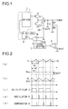
- Fig. 1 is a block diagram showing the internal configuration of the switching power supply apparatus of this embodiment.
- the switching power supply apparatus shown in Fig. 1 includes a p-channel MOS transistor Tr1 having a source to which a supply potential is applied, an n-channel MOS transistor Tr2 having a source to which a ground potential is applied, a driver 1 that feeds a signal to the gates of the MOS transistors Tr1 and Tr2 and thereby controls on/off thereof, a coil L that is connected, at one end thereof, to a node at which the drains of the MOS transistors Tr1 and Tr2 are connected together, a capacitor C that is connected, at one end thereof, to the other end of the coil L, and is grounded at the other end thereof, resistances R1 and R2 that are connected in series between a node at which the coil L and the capacitor C are connected together and the ground potential, a differential amplifier 2 that receives the voltage obtained by dividing the voltage appearing at the node at which the coil L and the capacitor C are connected together by the resistances R1 and R2, and receives a reference voltage Vref, a level shifter 3
- the driver 1 and the RS flip-flop 5 constitutes a control circuit 7, and a voltage source 20 that adds an offset voltage Voff (for example, 30 mV) to the voltage indicating the detected current value flowing through the coil L is connected to an inverting input terminal of the comparator 4. That is, when a current value IL flowing through the coil L is converted into a voltage value VL and is then inputted to the inverting input terminal of the comparator 4, the offset voltage Voff from the voltage source 20 is added thereto. Then, in the comparator 4, the voltage value VL to which the offset voltage Voff is added is compared with a voltage Vth that is fed back through the differential amplifier 2 and the level shifter 3 to a non-inverting input terminal of the comparator 4.
- Voff for example, 30 mV
- this switching power supply apparatus when a heavy load is connected to an output terminal OUT that is a node at which the coil L and the capacitor C are connected together, this switching power supply apparatus operates in the same manner as a conventional switching power supply apparatus.
- a transition diagram showing the transition of the signals of relevant parts is shown in Fig. 2.
- Fig. 2(d) when a high-level clock signal is fed from the oscillator 6 to the set terminal of the RS flip-flop 5, the output of the RS flip-flop 5 turns to high level, as shown in Fig. 2(c), whereby the driver 1 turns the MOS transistor Tr1 on and the MOS transistor Tr2 off.
- a current flows from the MOS transistor Tr1 to the coil L, and thus the current value IL flowing through the coil L increases, as shown in Fig. 2(a).
- the voltage VL inputted to the inverting input terminal of the comparator 4 decreases.
- a current value I0 shown in Fig. 2(a) indicates an average current value IL flowing through the coil L.
- the output voltage appearing at the output terminal OUT is divided by the resistances R1 and R2, and the voltage thus obtained is then fed back to the differential amplifier 2, where the difference between the voltage thus obtained and the reference voltage Vref is amplified, and then a voltage signal indicating an error between a feedback voltage indicating the output voltage and the reference voltage Vref is outputted. Then, this voltage signal is fed to the level shifter 3, where it is level shifted to a supply potential side.
- the voltage Vth fed from the level shifter 3 to the non-inverting input terminal of the comparator 4 indicates the output voltage appearing at the output terminal OUT.
- the output of the RS flip-flop 4 turns to low level, as shown in Fig. 2(c), whereby the driver 1 turns the MOS transistor Tr1 off and the MOS transistor Tr2 on.
- the current value IL flowing through the coil L decreases, and current begins to flow from the coil L to the MOS transistor Tr2.
- the voltage VL inputted to the inverting input terminal of the comparator 4 increases.
- a substantially constant direct-current voltage is outputted from the output terminal OUT to the load. That is, by adjusting the duration ta for which the MOS transistor Tr1 is turned on relative to a time period tb of the clock signal outputted from the oscillator 6 based on the result of comparison between the current value flowing through the coil L and the output voltage of the output terminal OUT, it is possible to keep the output voltage of the output terminal OUT constant.
- the voltage obtained by detecting the current IL flowing through the coil L is sufficiently higher than the offset voltage Voff from the voltage source 20. That is, the offset voltage Voff falls within the voltage range in which the influence thereof on the voltage VL inputted to the inverting input terminal of the comparator 4 is so small that it can be ignored.
- the RS flip-flop 5 continues to output a low-level signal, as shown in Fig. 3(c), because a high-level signal is inputted from the comparator 4 to the reset terminal of the RS flip-flop 5, as shown in Fig. 3(e).
- the drive 1 keeps the MOS transistor Tr1 off and the MOS transistor Tr2 on.
- the drive 1 turns the MOS transistor Tr1 on and the MOS transistor Tr2 off, whereby a current begins to flow through the coil L, as shown in Fig. 3(a).
- the voltage VL inputted to the inverting input terminal of the comparator 4 is dropped by the current IL flowing through the coil L.
- the voltage VL inputted to the inverting input terminal of the comparator 4 decreases, as shown in Fig. 3(b).
- the signal from the comparator 4 is switched to high level, as shown in Fig. 3(e).
- the signal from the RS flip-flop 5 turns to low level, as shown in Fig. 3(c).
- the signal from the RS flip-flop 5 turns to low level
- the driver 1 turns the MOS transistor Tr1 off and the MOS transistor Tr2 on
- the current value IL flowing through the coil L decreases, as shown in Fig. 3(a).
- the energy stored in the coil L is released, whereby the capacitor C is charged, and thus the output voltage from the output terminal OUT increases.
- the voltage Vth from the level shifter 3 increases.
- the capacitor C is discharged again, whereby the output voltage from the output terminal OUT decreases. In this way, the aforementioned operation is repeated.
- Fig. 4 shows an example of the configuration of a current detection circuit 10 that detects the level of a current flowing through the coil L and then converts it into a voltage value in the switching power supply apparatus described above. That is, the current detection circuit 10 is built with a p-channel MOS transistor Tra having a gate and a drain connected respectively to the gate and the drain of the MOS transistor Tr1 and a p-channel MOS transistor Trb having a drain connected to the source of the MOS transistor Tra, a source receiving a supply potential, and a gate receiving a reference potential.
- the MOS transistor Trb functions as a resistance.
- the MOS transistor Tra is made to operate.
- the voltage appearing at a node at which the drains of the MOS transistors Tr1 and Tr2 are connected together is fed to the drain of the MOS transistor Tra, and the current proportional to the current flowing through the MOS transistor Tr1 flows through the MOS transistors Tra and Trb.
- the voltage drop across the ON resistance of the MOS transistor Trb appears as a value proportional to the current value proportional to the current flowing through the MOS transistor Tr1, that is, a value proportional to the current value flowing through the coil L.
- the voltage drop across the ON resistance of the MOS transistor Trb appears, as a detected current value of the coil L, at a node at which the source of the MOS transistor Tra and the drain of the MOS transistor Trb are connected together, and is then fed to the inverting input terminal of the comparator 4.
- a resistance Ra is connected, at one end thereof, to the inverting input terminal of the comparator 4 and, at the other end thereof, to a node at which the source of the MOS transistor Tra and the drain of the MOS transistor Trb are connected together, and a constant-current power supply 11 that feeds a constant current is connected to the inverting input terminal of the comparator 4.
- the other end of the constant-current power supply 11 is grounded.
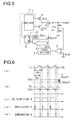
- Fig. 5 is a block diagram showing the internal configuration of the switching power supply apparatus of this embodiment.
- such devices and circuit blocks as serve the same purpose as those of the switching power supply apparatus shown in Fig. 1 do are identified with the same reference characters, and their detailed explanations will not be repeated.
- the switching power supply apparatus shown in Fig. 5 includes, instead of a voltage source 20 provided in the switching power supply apparatus shown in Fig. 1, a voltage source 20a for adding an offset voltage Vxoff that is switchable depending on an output of a comparator 4. That is, when a current value IL flowing through a coil L is converted into a voltage value VL and is then inputted to the inverting input terminal of the comparator 4, the offset voltage Vxoff from the voltage source 20a is added thereto.
- the value of the offset voltage Vxoff from the voltage source 20a becomes Vhoff (for example, 30 mV); when the output of the comparator 4 turns to low level, the value of the offset voltage Vxoff from the voltage source 20a becomes Vloff(for example, 20 mV).
- Vhoff for example, 30 mV
- Vloff for example, 20 mV
- the operation performed when a heavy load is connected to an output terminal OUT that is a node at which the coil L and a capacitor C are connected together will be first described below.
- This switching power supply apparatus operates in the same manner as the switching power supply apparatus (Fig. 1) of the first embodiment except that the value of the voltage VL is switched when the value of the offset voltage Vxoff from the voltage source 20a is switched depending on the output of the comparator 4. Therefore, in the following descriptions, emphasis will be placed on the operation performed when the output of the comparator 4 is switched. For operations of the other circuit blocks, reference should be made to the descriptions of the first embodiment.
- FIG. 6 A transition diagram showing the transition of the signals of relevant parts of the switching power supply apparatus of this embodiment is shown in Fig. 6.
- Fig. 6(a) when a current flows from a MOS transistor Tr1 to the coil L, and thus the current value IL flowing through the coil L increases, as shown in Fig. 6(a), the voltage VL inputted to the inverting input terminal of the comparator 4 decreases, as shown in Fig. 6(b).
- Fig. 6(a) the voltage VL inputted to the inverting input terminal of the comparator 4 decreases, as shown in Fig. 6(b).
- the voltage obtained by detecting the current IL flowing through the coil L is sufficiently higher than the offset voltage Vxoff from the voltage source 20. That is, the voltage values Vhoff and Vloff added as an offset voltage Vxoff each fall within the voltage range in which the influence thereof on the voltage VL inputted to the inverting input terminal of the comparator 4 is so small that it can be ignored.
- a low-level signal is outputted from the comparator 4.
- the value of the offset voltage Vxoff from the voltage source 20a becomes Vloff
- the voltage VL fed to the inverting input terminal of the comparator 4 becomes a value given by Vcc - Vloff, the value obtained by dropping the supply voltage Vcc by the offset voltage Vloff.
- a high-level clock signal is outputted from the oscillator 6, as shown in Fig. 7(d)
- the signal from the comparator 4 is switched to low level
- the signal from the RS flip-flop 5 is switched to high level, as shown in Fig. 7(c).
- a current detection circuit 10 having the same configuration as that shown in Fig. 4 of the first embodiment is incorporated in the switching power supply apparatus described above, the relation of connection between the current detection circuit 10 and the comparator 4 is shown in Fig. 8.
- a resistance Ra used for adding an offset voltage Voff is replaced with a variable resistance Rb that can switch a resistance value depending on the output of the comparator 4. That is, the variable resistance Rb and the constant-current power supply 11 constitute a voltage source 21a.
- Other circuit blocks are the same as those in Fig. 4.
- the resistance value of the variable resistance Rb is switched depending on the output of the comparator 4 in such a way that the resistance value obtained when the output of the comparator 4 turns to high level becomes greater than the resistance value obtained when the output of the comparator 4 turns to low level.
- the offset voltage Vxoff appearing due to the voltage drop across the variable resistance Rb is switched depending on the output of the comparator 4.
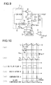
- Fig. 9 is a block diagram showing the internal configuration of the switching power supply apparatus of this embodiment.
- such devices and circuit blocks as serve the same purpose as those of the switching power supply apparatus shown in Fig. 1 do are identified with the same reference characters, and their detailed explanations will not be repeated.
- the switching power supply apparatus shown in Fig. 9 differs from the switching power supply apparatus shown in Fig. 1 in that a slope compensation signal having a time period tb for performing slope compensation is outputted from an oscillator 6, and a voltage source 21 whose voltage value varies depending on the slope compensation signal is provided between the inverting input terminal of a comparator 4 and a voltage source 20.
- a slope compensation signal having a time period tb for performing slope compensation is outputted from an oscillator 6, and a voltage source 21 whose voltage value varies depending on the slope compensation signal is provided between the inverting input terminal of a comparator 4 and a voltage source 20.
- This switching power supply apparatus operates in the same manner as the switching power supply apparatus (Fig. 1) of the first embodiment except that the value of the voltage VL varies depending on the slope compensation voltage Vslope. That is, a slope compensation voltage Vslope from the voltage source 21, the slop compensation voltage Vslope varying as shown in Fig. 10(f), and an offset voltage Voff from the voltage source 20 are subtracted from the voltage value obtained from the detected current IL of the coil L, the detected current IL shown in Fig. 10(a), whereby a voltage VL shown in Fig. 10(b) is inputted to the inverting input terminal of the comparator 4.
- a clock signal that is turned to high level at intervals of a time period tb as shown in Fig. 10(d) and a slope compensation signal having the same time period tb as this clock signal are outputted from the oscillator 6.
- the slope compensation voltage Vslope from the voltage source 21 gradually increases, and after reaching a maximum value VSmax (for example, 20 mV), it decreases until it reaches a minimum value of zero.
- a clock signal is outputted from the oscillator 6.
- the slope compensation voltage Vslope from the voltage source 21 varies in a roughly triangular wave pattern at intervals of a time period tb, as shown in Fig. 10(f).
- the slope compensation voltage Vslope from the voltage source 21 varies as shown in Fig. 10(f).
- the rate of change of the voltage VL is greater than that of the first embodiment, as shown in Fig. 10(b).
- the rate of change of the voltage VL is smaller than that of the first embodiment, as shown in Fig. 10(b).
- the value of the slope compensation voltage Vslope from the voltage source 21 changes from VSmax to zero, as shown in Fig. 10(f).
- the voltage VL increases by the voltage value VSmax, as shown in Fig. 10(b).
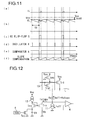
- the operation performed when no load or a light load is connected to the output terminal OUT will be described with reference to Fig. 11.
- the operation is the same as that of the switching power supply apparatus (Fig. 1) of the first embodiment except that the value of the voltage VL varies depending on the slope compensation voltage Vslope. That is, a slope compensation voltage Vslope from the voltage source 21, the slope compensation voltage Vslope varying as shown in Fig. 11(f), and an offset voltage Voff from the voltage source 20 are subtracted from the voltage value obtained from the detected current IL of the coil L, the detected current IL shown in Fig. 11(a), whereby the voltage VL shown in Fig. 11(b) is inputted to the inverting input terminal of the comparator 4.
- the slope compensation voltage Vslope from the voltage source 21 shown in Fig. 11(f) varies in the same manner as in Fig. 10(f).
- the RS flip-flop 5 continues to output a low-level signal, as shown in Fig. 11(c), because a high-level signal is inputted from the comparator 4 to the reset terminal of the RS flip-flop 5, as shown in Fig. 11(e). Meanwhile, the output voltage of the output terminal OUT decreases, and the voltage value of the voltage Vth outputted from the level shifter 3 gradually decreases, as shown in Fig. 11(b).
- a low-level signal is outputted from the comparator 4, and, immediately after the slope compensation voltage Vslope decreases from a maximum value VSmax to a minimum value of zero, a high-level clock signal is outputted from the oscillator 6, as shown in Fig. 7(d).
- a high-level signal is inputted to the set terminal of the RS flip-flop 5 after a low-level signal is inputted to the reset terminal thereof, whereby the signal from the RS flip-flop 5 is switched to high level, as shown in Fig. 11(c).
- the slope compensation voltage Vslope reaches to a minimum value of zero, it gradually increases again, as shown in Fig. 11(f).
- the slope compensation voltage Vslope increases, the voltage VL fed to the inverting input terminal of the comparator 4 decreases.
- the current source 21 is built with an n-channel MOS transistor Trx that is connected, at the drain thereof, to a node at which the resistance Ra and the constant-current power supply 11 are connected together, a MOS transistor Try that is connected, at the gate and the drain thereof, to the gate of the MOS transistor Trx, a MOS transistor Trz that is connected, at the drain thereof, to the source of the MOS transistor Try, a resistance Rc that is connected to the source of the MOS transistor Trx, a capacitor C 1 that is connected to the source of the MOS transistor Try, and a constant-current power supply 12 that is connected to the drain of the MOS transistor Trx.
- Other circuit blocks are the same as those in Fig. 4.
- the voltage Vslope generated by the current source 21 is obtained from the voltage drop given by Ra ⁇ Islope, the voltage drop across the resistance Ra caused by the passage of a current Islope through the MOS transistor Trx.
- the voltage Voff generated by the current source 20 is obtained from the voltage drop given by Ra ⁇ Ioff, the voltage drop across the resistance Ra caused by the passage of a current Ioff through the constant-current power supply 11.
- the slope compensation voltage Vslope appears across the resistance Ra, and this slope compensation voltage Vslope is added to the voltage VL inputted to the inverting input terminal of the comparator 4. That is, assume that the supply voltage is Vcc, the ON resistance of the MOS transistor Trb is Rx, and the current value flowing through the MOS transistor Tra relative to the current value IL of the coil L is A ⁇ IL.
- adding a slope compensation voltage to a voltage value indicating the detected current of the coil L offers the following advantages.
- the duty ratio i.e., the ratio of the duration of time that the MOS transistor Tr1 is turned on
- the comparator 4 output low level in synchronism with the reception of a clock signal, achieving more efficient operations than those of the first embodiment.
- this embodiment deals with an example in which a constant offset voltage Voff is added by the voltage source 20.
- a voltage source 20a that switches an offset voltage Vxoff depending on the output of the comparator 4.
- Fig. 13A a stepping-up switching power supply apparatus configured as shown in Fig. 13A
- Fig. 13B an inverting switching power supply apparatus configured as shown in Fig. 13B.
- Figs. 13A and 13B respectively show the configurations of the stepping-up and inverting switching power supply apparatuses applied to the switching power supply apparatus of the first embodiment
- the stepping-up and inverting switching power supply apparatuses can be applied to the switching power supply apparatus of the second or third embodiment.
- the stepping-up switching power supply apparatus as shown in Fig. 13A includes a coil L that receives a supply potential at one end thereof, an n-channel MOS transistor Trn that is connected, at the drain thereof, to the other end of the coil L and is controlled by a driver 1a, a diode D that is connected, at the anode thereof, to the drain of the MOS transistor Trn, and a capacitor C that is connected, at one end thereof, to the cathode of the diode D.
- the current flowing through the coil L or the MOS transistor Trn is fed back to the inverting input terminal of a comparator 4 as a voltage value.
- an offset voltage Voff is added thereto by a voltage source 20.
- the inverting switching power supply apparatus shown in Fig. 13B includes a coil L that is grounded at one end thereof, a p-channel MOS transistor Trp that is connected, at the drain thereof, to the other end of the coil L and is controlled by a driver 1b, a diode D that is connected, at the cathode thereof, to the drain of the MOS transistor Trp, and a capacitor C that is connected, at one end thereof, to the anode of the diode D.
- the current flowing through the coil L or the MOS transistor Trp is fed back to the inverting input terminal of a comparator 4 as a voltage value.
- an offset voltage Voff is added thereto by a voltage source 20.
- the embodiments described above deal with cases in which relevant circuit blocks are made to operate based on a supply potential; instead, they may be made to operate based on a ground potential.
- the relevant circuit blocks can be basically so configured as to have the same configurations as those of the embodiments described above.
- the embodiments described above deal with cases in which the output from the differential amplifier is inputted to the comparator via the level shifter. However, the output from the differential amplifier may be directly inputted to the comparator without involving the level shifter.
- a switching power supply apparatus of the present invention can be applied to mobile devices such as mobile phones or mobile terminal devices, and, in these mobile devices, it serves as a switching power supply apparatus that transforms the voltage from a rechargeable battery and then feeds it to other circuit arrangements.
- the switching power supply apparatus By configuring the switching power supply apparatus as in the present invention, when the load condition enters light or no load by turning off the other circuit arrangements of the mobile device, it is possible to make the switching power supply apparatus operate with a high degree of efficiency, and thereby to reduce power consumption.
Landscapes
- Engineering & Computer Science (AREA)
- Power Engineering (AREA)
- Dc-Dc Converters (AREA)
Abstract
Description
- The present invention relates to a switching power supply apparatus that reduces the loss at light load and thus improves efficiency. More particularly, the present invention relates to a switching power supply apparatus that adopts current mode by which switching control is performed by detecting a coil current on an output side, and a mobile device that incorporates the switching power supply apparatus and achieves low power consumption.
- Conventionally, in a switching power supply apparatus that controls the amount of current to be fed to a load by controlling on/off of a built-in switching device, intermittent control is employed that permits switching to an intermittent switching operation having the duration for which a switching operation of the switching device is stopped in order to reduce the loss of the switching power supply apparatus at light load (see Patent Publication 1). The switching power supply apparatus performing the aforementioned intermittent control is provided with a comparator that compares a voltage commensurate with an output voltage with a reference voltage Vburst for intermittent control.
- When the comparator finds the voltage commensurate with the output voltage to be higher than the reference voltage Vburst because of light load, the switching control operation of the switching device performed by a driver is stopped. Then, because of hysteresis exhibited by the comparator, when the comparator finds the output voltage to be lower, the switching control operation of the switching device performed by the driver is resumed. By repeating such an operation at light load, the intermittent control by the comparator for intermittent control is performed, whereby the efficiency of the intermittent control is increased.
Patent Publication 1:JP-A-H06-303766 - However, this conventional switching power supply apparatus needs to be provided with a comparator for intermittent control for intermittently performing a switching operation of a switching device by a driver to increase efficiency at light load. This additional comparator for intermittent control increases the size of the circuitry constituting the switching power supply apparatus, and thus hinders miniaturization of a mobile device in which the switching power supply apparatus is incorporated.
- In view of the conventionally experienced inconveniences and disadvantages described above, an object of the present invention is to provide a switching power supply apparatus that can maintain high efficiency without requiring an additional circuit for intermittent control at light load.
- To achieve the above object, according to the present invention, a switching power supply apparatus is provided with: a switching device for performing an on/off operation; a control circuit for controlling on/off of the switching device; a coil, a level of a current flowing therethrough being controlled by the switching device; a capacitor that is connected to the coil and that performs rectification together with the coil; and an oscillator for outputting to the control circuit an oscillating signal at intervals of a fixed time period for turning the switching device on. This switching power supply apparatus outputs an output voltage from a node at which the capacitor and the coil are connected together, and further includes: a current detection portion for detecting a current value flowing through the coil, converting the detected current value into a voltage value, and then outputting the voltage value thus obtained as a current detection voltage; a voltage source for adding an offset voltage to the current detection voltage from the current detection portion; and a comparator for comparing the current detection voltage to which the offset voltage is added by the voltage source with a voltage commensurate with the difference between a voltage commensurate with the output voltage and a reference voltage. Here, if the comparator finds the magnitude of the current detection voltage to which the offset voltage is added to be greater than the voltage commensurate with the difference between the voltage commensurate with the output voltage and the reference voltage, the oscillating signal from the oscillator is masked, and the switching device is turned off.
- According to the present invention, at no load or light load in which the difference between an output voltage and a reference voltage is small, adding an offset voltage to a current detection voltage indicating a detected current value flowing through a coil makes it possible for a comparator to find the magnitude of the current detection voltage to be greater than the difference between the output voltage and the reference voltage. In that case, an oscillating signal outputted from an oscillator for turning a switching device on can be masked. This makes it possible to perform intermittent control of a switching operation of the switching device until the difference between the output voltage and the reference voltage becomes greater. Thus, unlike the conventional example, there is no need to add a comparator for intermittent control. This makes it possible to maintain high efficiency at light load or no load, and achieve miniaturization of an apparatus.
-
- [Fig. 1] A block diagram showing the internal configuration of the switching power supply apparatus of a first embodiment.
- [Fig. 2] A timing chart showing how relevant parts of the switching power supply apparatus shown in Fig. 1 operate at heavy load.
- [Fig. 3] A timing chart showing how relevant parts of the switching power supply apparatus shown in Fig. 1 operate at light load or no load.
- [Fig. 4] A circuit diagram showing an example of the configuration of the current detection circuit and a portion surrounding it in the switching power supply apparatus shown in Fig. 1.
- [Fig. 5] A block diagram showing the internal configuration of the switching power supply apparatus of a second embodiment.
- [Fig. 6] A timing chart showing how relevant parts of the switching power supply apparatus shown in Fig. 5 operate at heavy load.
- [Fig. 7] A timing chart showing how relevant parts of the switching power supply apparatus shown in Fig. 5 operate at light load or no load.
- [Fig. 8] A circuit diagram showing an example of the configuration of the current detection circuit and a portion surrounding it in the switching power supply apparatus shown in Fig. 5.
- [Fig. 9] A block diagram showing the internal configuration of the switching power supply apparatus of a third embodiment.
- [Fig. 10] A timing chart showing how relevant parts of the switching power supply apparatus shown in Fig. 9 operate at heavy load.
- [Fig. 11] A timing chart showing how relevant parts of the switching power supply apparatus shown in Fig. 9 operate at light load or no load.
- [Fig. 12] A circuit diagram showing an example of the configuration of the current detection circuit and a portion surrounding it in the switching power supply apparatus shown in Fig. 9.
- [Fig. 13A] A block diagram showing an example of the configuration of the apparatus applied to a stepping-up switching power supply apparatus.
- [Fig. 13B] A block diagram showing an example of the configuration of the apparatus applied to an inverting switching power supply apparatus.
-
- 1
- driver
- 2
- differential amplifier
- 3
- level shifter
- 4
- comparator
- 5
- RS flip-flop
- 6
- oscillator
- 20, 20a, 21
- voltage source
- Tr1, Tr2
- MOS transistor
- L
- coil
- C
- capacitor
- R1, R2
- resistance
- Hereinafter, a first embodiment of the present invention will be described with reference to the accompanying drawings. Fig. 1 is a block diagram showing the internal configuration of the switching power supply apparatus of this embodiment.
- The switching power supply apparatus shown in Fig. 1 includes a p-channel MOS transistor Tr1 having a source to which a supply potential is applied, an n-channel MOS transistor Tr2 having a source to which a ground potential is applied, a driver 1 that feeds a signal to the gates of the MOS transistors Tr1 and Tr2 and thereby controls on/off thereof, a coil L that is connected, at one end thereof, to a node at which the drains of the MOS transistors Tr1 and Tr2 are connected together, a capacitor C that is connected, at one end thereof, to the other end of the coil L, and is grounded at the other end thereof, resistances R1 and R2 that are connected in series between a node at which the coil L and the capacitor C are connected together and the ground potential, a differential amplifier 2 that receives the voltage obtained by dividing the voltage appearing at the node at which the coil L and the capacitor C are connected together by the resistances R1 and R2, and receives a reference voltage Vref, a level shifter 3 that level shifts the output voltage from the error amplifier 2, a comparator 4 that compares the voltage from the level shifter 3 with the voltage indicating the current flowing through the coil L, an RS flip-flop 5 that receives, at a reset terminal thereof, an output from the comparator 4, and an oscillator 6 that inputs a signal to a set terminal of the RS flip-flop 5.
- The
driver 1 and the RS flip-flop 5 constitutes acontrol circuit 7, and avoltage source 20 that adds an offset voltage Voff (for example, 30 mV) to the voltage indicating the detected current value flowing through the coil L is connected to an inverting input terminal of thecomparator 4. That is, when a current value IL flowing through the coil L is converted into a voltage value VL and is then inputted to the inverting input terminal of thecomparator 4, the offset voltage Voff from thevoltage source 20 is added thereto. Then, in thecomparator 4, the voltage value VL to which the offset voltage Voff is added is compared with a voltage Vth that is fed back through thedifferential amplifier 2 and thelevel shifter 3 to a non-inverting input terminal of thecomparator 4.
In the switching power supply apparatus configured as described above, when a heavy load is connected to an output terminal OUT that is a node at which the coil L and the capacitor C are connected together, this switching power supply apparatus operates in the same manner as a conventional switching power supply apparatus. A transition diagram showing the transition of the signals of relevant parts is shown in Fig. 2. As shown in Fig. 2(d), when a high-level clock signal is fed from theoscillator 6 to the set terminal of the RS flip-flop 5, the output of the RS flip-flop 5 turns to high level, as shown in Fig. 2(c), whereby thedriver 1 turns the MOS transistor Tr1 on and the MOS transistor Tr2 off. - As a result, a current flows from the MOS transistor Tr1 to the coil L, and thus the current value IL flowing through the coil L increases, as shown in Fig. 2(a). Thus, as shown in Fig. 2(b), the voltage VL inputted to the inverting input terminal of the
comparator 4 decreases. Note that a current value I0 shown in Fig. 2(a) indicates an average current value IL flowing through the coil L. As shown in Fig. 2(b), if the voltage VL becomes lower than the voltage Vth inputted from thelevel shifter 3 to the non-inverting input terminal of thecomparator 4 when time ta has elapsed after reception of the high-level clock signal from theoscillator 6, a high-level signal is outputted from thecomparator 4, as shown in Fig. 2(e). - Incidentally, the output voltage appearing at the output terminal OUT is divided by the resistances R1 and R2, and the voltage thus obtained is then fed back to the
differential amplifier 2, where the difference between the voltage thus obtained and the reference voltage Vref is amplified, and then a voltage signal indicating an error between a feedback voltage indicating the output voltage and the reference voltage Vref is outputted. Then, this voltage signal is fed to thelevel shifter 3, where it is level shifted to a supply potential side. As a result, when the output voltage appearing at the output terminal OUT increases, the voltage from thedifferential amplifier 2 decreases, and thus the voltage value of the voltage Vth outputted from thelevel shifter 3 increases. As described above, the voltage Vth fed from thelevel shifter 3 to the non-inverting input terminal of thecomparator 4 indicates the output voltage appearing at the output terminal OUT. - Since the high-level signal is inputted from the
comparator 4 to the reset terminal of the RS flip-flop 5, the output of the RS flip-flop 4 turns to low level, as shown in Fig. 2(c), whereby thedriver 1 turns the MOS transistor Tr1 off and the MOS transistor Tr2 on. As a result, as shown in Fig. 2(a), the current value IL flowing through the coil L decreases, and current begins to flow from the coil L to the MOS transistor Tr2. Thus, as shown in Fig. 2(b), the voltage VL inputted to the inverting input terminal of thecomparator 4 increases. When time tb has elapsed after reception of the high-level clock signal from theoscillator 6, a next clock signal is outputted from theoscillator 6, as shown in Fig. 2(d). In this way, the aforementioned operation is repeated. - By repeating the operation described above, a substantially constant direct-current voltage is outputted from the output terminal OUT to the load. That is, by adjusting the duration ta for which the MOS transistor Tr1 is turned on relative to a time period tb of the clock signal outputted from the
oscillator 6 based on the result of comparison between the current value flowing through the coil L and the output voltage of the output terminal OUT, it is possible to keep the output voltage of the output terminal OUT constant. It is to be noted that, when a heavy load is connected as described above, the voltage obtained by detecting the current IL flowing through the coil L is sufficiently higher than the offset voltage Voff from thevoltage source 20. That is, the offset voltage Voff falls within the voltage range in which the influence thereof on the voltage VL inputted to the inverting input terminal of thecomparator 4 is so small that it can be ignored. - Now, an operation performed when no load or a light load is connected to the output terminal OUT will be described below with reference to Fig. 3. In this case, since the output voltage appearing at the output terminal OUT increases, and thus an error between the divided voltage obtained by the resistances R1 and R2 and the reference voltage Vref becomes smaller, the voltage from the
differential amplifier 2 decreases. This makes high the voltage value of the voltage Vth outputted from thelevel shifter 3, as shown in Fig. 3(b). As described above, the voltage Vth fed from thelevel shifter 3 to the non-inverting input terminal of thecomparator 4 indicates the output voltage appearing at the output terminal OUT. - At this time, since the MOS transistor Tr1 is turned off and the MOS transistor Tr2 is turned on, and no current flows through the coil L, as shown in Fig. 3(a), the voltage VL fed to the inverting input terminal of the
comparator 4 becomes a value given by Vcc - Voff, the value obtained by dropping a supply voltage Vcc by the offset voltage Voff fed from thevoltage source 20. As shown in Fig. 3(b), when the voltage Vth outputted from thelevel shifter 3 is higher than the voltage VL (= Vcc - Voff), a high-level signal is outputted from thecomparator 4. - Thus, as shown in Fig. 3(d), even when a high-level clock signal is outputted from the
oscillator 6 at intervals of a time period tb, the RS flip-flop 5 continues to output a low-level signal, as shown in Fig. 3(c), because a high-level signal is inputted from thecomparator 4 to the reset terminal of the RS flip-flop 5, as shown in Fig. 3(e). Thus, thedrive 1 keeps the MOS transistor Tr1 off and the MOS transistor Tr2 on. - At this time, since the capacitor C is discharged, the output voltage of the output terminal OUT decreases. As a result, as shown in Fig. 3(b), the voltage value of the voltage Vth outputted from the
level shifter 3 gradually decreases. When the voltage Vth outputted from thelevel shifter 3 becomes lower than the voltage VL (= Vcc - Voff), a low-level signal is outputted from thecomparator 4, as shown in Fig. 3(e). As described above, when a high-level clock signal is outputted from theoscillator 6, as shown in Fig. 3(d), after the signal from thecomparator 4 is switched to low level, the signal from the RS flip-flop 5 is switched to high level, as shown in Fig. 3(c). - Thus, the
drive 1 turns the MOS transistor Tr1 on and the MOS transistor Tr2 off, whereby a current begins to flow through the coil L, as shown in Fig. 3(a). As a result, the voltage VL inputted to the inverting input terminal of thecomparator 4 is dropped by the current IL flowing through the coil L. As the current IL flowing through the coil L increases, as shown in Fig. 3(a), the voltage VL inputted to the inverting input terminal of thecomparator 4 decreases, as shown in Fig. 3(b). When the voltage VL becomes lower than the voltage Vth from thelevel shifter 3, as shown in Fig. 3(b), the signal from thecomparator 4 is switched to high level, as shown in Fig. 3(e). As a result, the signal from the RS flip-flop 5 turns to low level, as shown in Fig. 3(c). - As described above, the signal from the RS flip-
flop 5 turns to low level, thedriver 1 turns the MOS transistor Tr1 off and the MOS transistor Tr2 on, and the current value IL flowing through the coil L decreases, as shown in Fig. 3(a). At this time, the energy stored in the coil L is released, whereby the capacitor C is charged, and thus the output voltage from the output terminal OUT increases. As a result, as shown in Fig. 3(b), the voltage Vth from thelevel shifter 3 increases. After that, the capacitor C is discharged again, whereby the output voltage from the output terminal OUT decreases. In this way, the aforementioned operation is repeated. - By repeating the operation described above, it is possible to mask the clock signal from the
oscillator 6 by feeding a high-level signal to the reset terminal of the RS flip-flop 5 while the voltage from the output terminal OUT is higher than a predetermined voltage. This makes it possible to make the duration for which the MOS transistor Tr1 is turned on longer than that obtained under heavy load conditions, and make the duty ratio, i.e., the ratio of the duration of time that the MOS transistor Tr1 is turned on, smaller than that obtained under heavy load conditions. That is, by performing a switching operation, which is performed at heavy load at intervals of a time period tb, once in a plurality of periods, it is possible to improve efficiency at no load or light load. - Fig. 4 shows an example of the configuration of a
current detection circuit 10 that detects the level of a current flowing through the coil L and then converts it into a voltage value in the switching power supply apparatus described above. That is, thecurrent detection circuit 10 is built with a p-channel MOS transistor Tra having a gate and a drain connected respectively to the gate and the drain of the MOS transistor Tr1 and a p-channel MOS transistor Trb having a drain connected to the source of the MOS transistor Tra, a source receiving a supply potential, and a gate receiving a reference potential. - In this configuration, the MOS transistor Trb functions as a resistance. When the same voltage as that fed to the gate of the MOS transistor Tr1 from the
driver 1 is fed to the gate of the MOS transistor Tra, the MOS transistor Tra is made to operate. At this time, the voltage appearing at a node at which the drains of the MOS transistors Tr1 and Tr2 are connected together is fed to the drain of the MOS transistor Tra, and the current proportional to the current flowing through the MOS transistor Tr1 flows through the MOS transistors Tra and Trb. - Then, the voltage drop across the ON resistance of the MOS transistor Trb appears as a value proportional to the current value proportional to the current flowing through the MOS transistor Tr1, that is, a value proportional to the current value flowing through the coil L. As described above, the voltage drop across the ON resistance of the MOS transistor Trb appears, as a detected current value of the coil L, at a node at which the source of the MOS transistor Tra and the drain of the MOS transistor Trb are connected together, and is then fed to the inverting input terminal of the
comparator 4. - Furthermore, as shown in Fig. 4, a resistance Ra is connected, at one end thereof, to the inverting input terminal of the
comparator 4 and, at the other end thereof, to a node at which the source of the MOS transistor Tra and the drain of the MOS transistor Trb are connected together, and a constant-current power supply 11 that feeds a constant current is connected to the inverting input terminal of thecomparator 4. The other end of the constant-current power supply 11 is grounded. In this way, by connecting the resistance Ra and the constant-current power supply 11 together, a voltage drop Ra × Ioff across the resistance Ra caused by the passage of a constant current Ioff fed from the constant-current power supply 11 through the resistance Ra is added as an offset voltage Voff. That is, the resistance Ra and the constant-current power supply 10 function as avoltage source 20. - Here, assume that the supply voltage is Vcc, the ON resistance of the MOS transistor Trb is Rx, and the current value flowing through the MOS transistor Tra relative to the current value IL of the coil L is A × IL. Then, a voltage given by Vcc - Rx × A × IL appears at a node at which the source of the MOS transistor Tra and the drain of the MOS transistor Trb are connected together. When the voltage given by Vcc - Rx × A × IL is outputted as an output of the
current detection circuit 10 and is then fed to one end of the resistance Ra, a voltage given by Vcc - Rx × A × IL - Ra × Ioff (= Vcc - Rx × A × IL - Voff), the voltage given an offset resulting from the voltage drop across the resistance Ra, is fed to the inverting input terminal of thecomparator 4 as a voltage VL. - A second embodiment of the present invention will be described with reference to the accompanying drawings. Fig. 5 is a block diagram showing the internal configuration of the switching power supply apparatus of this embodiment. In the following description of the switching power supply apparatus shown in Fig. 5, such devices and circuit blocks as serve the same purpose as those of the switching power supply apparatus shown in Fig. 1 do are identified with the same reference characters, and their detailed explanations will not be repeated.
- The switching power supply apparatus shown in Fig. 5 includes, instead of a
voltage source 20 provided in the switching power supply apparatus shown in Fig. 1, avoltage source 20a for adding an offset voltage Vxoff that is switchable depending on an output of acomparator 4. That is, when a current value IL flowing through a coil L is converted into a voltage value VL and is then inputted to the inverting input terminal of thecomparator 4, the offset voltage Vxoff from thevoltage source 20a is added thereto. At this time, when the output of thecomparator 4 turns to high level, the value of the offset voltage Vxoff from thevoltage source 20a becomes Vhoff (for example, 30 mV); when the output of thecomparator 4 turns to low level, the value of the offset voltage Vxoff from thevoltage source 20a becomes Vloff(for example, 20 mV). The relationship between the offset voltage Vhoff and the offset voltage Vloff is Vhoff > Vloff. - In the switching power supply apparatus configured as described above, the operation performed when a heavy load is connected to an output terminal OUT that is a node at which the coil L and a capacitor C are connected together will be first described below. This switching power supply apparatus operates in the same manner as the switching power supply apparatus (Fig. 1) of the first embodiment except that the value of the voltage VL is switched when the value of the offset voltage Vxoff from the
voltage source 20a is switched depending on the output of thecomparator 4. Therefore, in the following descriptions, emphasis will be placed on the operation performed when the output of thecomparator 4 is switched. For operations of the other circuit blocks, reference should be made to the descriptions of the first embodiment. - A transition diagram showing the transition of the signals of relevant parts of the switching power supply apparatus of this embodiment is shown in Fig. 6. As is the case with the first embodiment, when a current flows from a MOS transistor Tr1 to the coil L, and thus the current value IL flowing through the coil L increases, as shown in Fig. 6(a), the voltage VL inputted to the inverting input terminal of the
comparator 4 decreases, as shown in Fig. 6(b). As shown in Fig. 6(b), if the voltage VL becomes lower than the voltage Vth inputted from thelevel shifter 3 to the non-inverting input terminal of thecomparator 4 when time ta has elapsed after reception of the high-level clock signal from theoscillator 6, a high-level signal is outputted from thecomparator 4, as shown in Fig. 6(e). - As a result, since the offset voltage Vxoff from the
voltage source 20a is switched from a voltage value Vloff to a voltage value Vhoff, the voltage value of the voltage VL inputted to the inverting input terminal of thecomparator 4 decreases by Vhoff - Vloff, as shown in Fig. 6(b). On the other hand, as shown in Fig. 6(c), the signal from the RS flip-flop 5 turns to low level, whereby thedriver 1 turns the MOS transistor Tr1 off and the MOS transistor Tr2 on. As a result, the current value IL flowing through the coil L decreases, as shown in Fig. 6(a), and the voltage VL inputted to the inverting input terminal of thecomparator 4 increases, as shown in Fig. 6(b). - After that, when the voltage VL becomes higher than the voltage Vth inputted from the
level shifter 3 to the non-inverting input terminal of thecomparator 4, as shown in Fig. 6(b), a low-level signal is outputted from thecomparator 4, as shown in Fig. 6(e). As a result, the offset voltage Vxoff from thevoltage source 20a is switched from a voltage value Vhoff to a voltage value Vloff, whereby the voltage value of the voltage VL inputted to the inverting input terminal of thecomparator 4 increases by Vhoff - Vloff, as shown in Fig. 6(b). In this way, a switching operation of the offset voltage Vxoff of thevoltage source 20a is performed each time the signal from thecomparator 4 is switched. - As is the case of the first embodiment, also in this embodiment, when a heavy load is connected as described above, the voltage obtained by detecting the current IL flowing through the coil L is sufficiently higher than the offset voltage Vxoff from the
voltage source 20. That is, the voltage values Vhoff and Vloff added as an offset voltage Vxoff each fall within the voltage range in which the influence thereof on the voltage VL inputted to the inverting input terminal of thecomparator 4 is so small that it can be ignored. - Similarly, the operation performed when no load or a light load is connected to the output terminal OUT will be described with reference to Fig. 7. Also in this case, the operation is the same as that of the switching power supply apparatus (Fig. 1) of the first embodiment except that the value of the offset voltage Vxoff from the
voltage source 20a is switched depending on the output of thecomparator 4. Therefore, in the following descriptions, emphasis will be placed on the operation performed when the output of thecomparator 4 is switched. For operations of the other circuit blocks, reference should be made to the descriptions of the first embodiment. - As is the case with the first embodiment, as shown in Fig. 7(e), when the
comparator 4 outputs high level, the MOS transistor Tr1 is turned off and the MOS transistor Tr2 is turned on, and thus no current flows through the coil L, as shown in Fig. 7(a). As a result, the value of the offset voltage Vxoff from thevoltage source 20a becomes Vhoff, and, as shown in Fig. 7(b), the voltage VL fed to the inverting input terminal of thecomparator 4 becomes a value given by Vcc - Vhoff, the value obtained by dropping the supply voltage Vcc by the offset voltage Vhoff. At this time, as shown in Fig. 7(b), the voltage Vth outputted from thelevel shifter 3 is higher than the voltage VL (= Vcc - Vhoff). - Thus, as shown in Fig. 7(d), even when a high-level clock signal is outputted from the
oscillator 6 at intervals of a time period tb, the RS flip-flop 5 continues to output a low-level output signal, as shown in Fig. 7(c), because a high-level signal is inputted from thecomparator 4 to the reset terminal of the RS flip-flop 5, as shown in Fig. 7(e). Meanwhile, the output voltage of the output terminal OUT decreases, the voltage value of the voltage Vth outputted from thelevel shifter 3 gradually decreases, as shown in Fig. 7(b), and the voltage Vth outputted from thelevel shifter 3 becomes lower than the voltage VL (= Vcc - Vhoff). - At this time, as shown in Fig. 7(e), a low-level signal is outputted from the
comparator 4. Thus, the value of the offset voltage Vxoff from thevoltage source 20a becomes Vloff, and, as shown in Fig. 7(b), the voltage VL fed to the inverting input terminal of thecomparator 4 becomes a value given by Vcc - Vloff, the value obtained by dropping the supply voltage Vcc by the offset voltage Vloff. In this way, if a high-level clock signal is outputted from theoscillator 6, as shown in Fig. 7(d), after the signal from thecomparator 4 is switched to low level, the signal from the RS flip-flop 5 is switched to high level, as shown in Fig. 7(c). - As a result, since a current begins to flow through the coil L, as shown in Fig. 7(a), the voltage VL inputted to the inverting input terminal of the
comparator 4 drops by the current IL flowing through the coil L, as shown in Fig. 7(b). When the voltage VL becomes lower than the voltage Vth from thelevel shifter 3, as shown in Fig. 7(b), the signal from thecomparator 4 is switched to high level, as shown in Fig. 7(e), and thus the signal from the RS flip-flop 5 turns to low level, as shown in Fig. 7(c). On the other hand, since the offset voltage Vxoff from thevoltage source 20a is switched to Vhoff, the voltage VL inputted to the inverting input terminal of thecomparator 4 decreases by Vhoff- Vloff. - As described above, since the signal from the RS flip-
flop 5 turns to low level, the current value IL flowing through the coil L decreases, as shown in Fig. 7(a), and the voltage VL increases up to Vcc - Vhoff, as shown in Fig. 7(b). At this time, the energy stored in the coil L is released, whereby the capacitor C is charged, and thus the output voltage from the output terminal OUT increases. As a result, as shown in Fig. 7(b), the voltage Vth from thelevel shifter 3 increases. After that, the capacitor C is discharged again, whereby the output voltage from the output terminal OUT decreases. In this way, the aforementioned operation is repeated. - When a
current detection circuit 10 having the same configuration as that shown in Fig. 4 of the first embodiment is incorporated in the switching power supply apparatus described above, the relation of connection between thecurrent detection circuit 10 and thecomparator 4 is shown in Fig. 8. In this case, as shown in Fig. 8, a resistance Ra used for adding an offset voltage Voff is replaced with a variable resistance Rb that can switch a resistance value depending on the output of thecomparator 4. That is, the variable resistance Rb and the constant-current power supply 11 constitute a voltage source 21a. Other circuit blocks are the same as those in Fig. 4. - With this configuration, the resistance value of the variable resistance Rb is switched depending on the output of the
comparator 4 in such a way that the resistance value obtained when the output of thecomparator 4 turns to high level becomes greater than the resistance value obtained when the output of thecomparator 4 turns to low level. As a result, the offset voltage Vxoff appearing due to the voltage drop across the variable resistance Rb is switched depending on the output of thecomparator 4. The operations other than the resistance value switching operation performed by the variable resistance Rb are the same as in the first embodiment, and therefore no detailed description thereof will be repeated. For these operations, reference should be made to the descriptions of the first embodiment. - As described in this embodiment, by giving hysteresis to an offset voltage to be added to a voltage value indicating a detected current of the coil L by switching the offset voltage depending on the output of the
comparator 4, it is possible to make thecomparator 4 output a clock signal more reliably than the first embodiment. This helps prevent malfunctioning of the RS flip-flop 5. - A third embodiment of the present invention will be described with reference to the accompanying drawings. Fig. 9 is a block diagram showing the internal configuration of the switching power supply apparatus of this embodiment. In the following description of the switching power supply apparatus shown in Fig. 9, such devices and circuit blocks as serve the same purpose as those of the switching power supply apparatus shown in Fig. 1 do are identified with the same reference characters, and their detailed explanations will not be repeated.
- The switching power supply apparatus shown in Fig. 9 differs from the switching power supply apparatus shown in Fig. 1 in that a slope compensation signal having a time period tb for performing slope compensation is outputted from an
oscillator 6, and avoltage source 21 whose voltage value varies depending on the slope compensation signal is provided between the inverting input terminal of acomparator 4 and avoltage source 20. Thus, when a current value IL flowing through a coil L is converted into a voltage value VL and is then inputted to the inverting input terminal of thecomparator 4, an offset voltage Voff and a slope compensation voltage Vslope are added thereto. As described above, the operations of this embodiment are the same as those of the first embodiment except that a voltage value VL fed to the inverting input terminal of thecomparator 4 is different from that of the first embodiment. Therefore, in the following descriptions, emphasis will be placed on the relationship between the voltage value VL fed to the inverting input terminal of thecomparator 4 and the slope compensation voltage Vslope. For other circuit blocks, reference should be made to the descriptions of the first embodiment. - In the switching power supply apparatus configured as described above, the operation performed when a heavy load is connected to an output terminal OUT that is a node at which the coil L and a capacitor C are connected together will be first described below. This switching power supply apparatus operates in the same manner as the switching power supply apparatus (Fig. 1) of the first embodiment except that the value of the voltage VL varies depending on the slope compensation voltage Vslope. That is, a slope compensation voltage Vslope from the
voltage source 21, the slop compensation voltage Vslope varying as shown in Fig. 10(f), and an offset voltage Voff from thevoltage source 20 are subtracted from the voltage value obtained from the detected current IL of the coil L, the detected current IL shown in Fig. 10(a), whereby a voltage VL shown in Fig. 10(b) is inputted to the inverting input terminal of thecomparator 4. - At this time, a clock signal that is turned to high level at intervals of a time period tb as shown in Fig. 10(d) and a slope compensation signal having the same time period tb as this clock signal are outputted from the
oscillator 6. Thus, as shown in Fig. 10(f), during a time period tb, the slope compensation voltage Vslope from thevoltage source 21 gradually increases, and after reaching a maximum value VSmax (for example, 20 mV), it decreases until it reaches a minimum value of zero. As shown in Figs. 10(c) and 10(f), after the slope compensation voltage Vslope decreases from a maximum value VSmax to a minimum value of zero, a clock signal is outputted from theoscillator 6. As described above, the slope compensation voltage Vslope from thevoltage source 21 varies in a roughly triangular wave pattern at intervals of a time period tb, as shown in Fig. 10(f). - The slope compensation voltage Vslope from the
voltage source 21 varies as shown in Fig. 10(f). As a result, when the RS flip-flop 5 outputs high level as shown in Fig. 10(c), the rate of change of the voltage VL is greater than that of the first embodiment, as shown in Fig. 10(b). On the other hand, when the RS flip-flop 5 outputs low level as shown in Fig. 10(c), the rate of change of the voltage VL is smaller than that of the first embodiment, as shown in Fig. 10(b). When a clock signal is outputted from theoscillator 6, as shown in Fig. 10(d), and the output of the RS flip-flop 5 is switched from low level to high level, as shown in Fig. 10(c), the value of the slope compensation voltage Vslope from thevoltage source 21 changes from VSmax to zero, as shown in Fig. 10(f). As a result, the voltage VL increases by the voltage value VSmax, as shown in Fig. 10(b). - Similarly, the operation performed when no load or a light load is connected to the output terminal OUT will be described with reference to Fig. 11. Also in this case, the operation is the same as that of the switching power supply apparatus (Fig. 1) of the first embodiment except that the value of the voltage VL varies depending on the slope compensation voltage Vslope. That is, a slope compensation voltage Vslope from the
voltage source 21, the slope compensation voltage Vslope varying as shown in Fig. 11(f), and an offset voltage Voff from thevoltage source 20 are subtracted from the voltage value obtained from the detected current IL of the coil L, the detected current IL shown in Fig. 11(a), whereby the voltage VL shown in Fig. 11(b) is inputted to the inverting input terminal of thecomparator 4. Incidentally, the slope compensation voltage Vslope from thevoltage source 21 shown in Fig. 11(f) varies in the same manner as in Fig. 10(f). - As is the case with the first embodiment, as shown in Fig. 11(e), when the
comparator 4 outputs high level, the MOS transistor Tr1 is turned off and the MOS transistor Tr2 is turned on, and thus no current flows through the coil L, as shown in Fig. 11(a). As a result, as shown in Fig. 11(b), the voltage VL fed to the inverting input terminal of thecomparator 4 becomes a value given by Vcc - Voff - Vslope, the value obtained by dropping the supply voltage Vcc by the offset voltage Voff from thevoltage source 20 and the slope compensation voltage Vslope from thevoltage source 21, the slope compensation voltage Vslope shown in Fig. 11(f). At this time, as shown in Fig. 11(b), the voltage Vth outputted from thelevel shifter 3 is higher than the voltage VL (= Vcc - Voff - Vslope). - Thus, as shown in Fig. 11(d), even when a high-level clock signal is outputted from the
oscillator 6 at intervals of a time period tb, the RS flip-flop 5 continues to output a low-level signal, as shown in Fig. 11(c), because a high-level signal is inputted from thecomparator 4 to the reset terminal of the RS flip-flop 5, as shown in Fig. 11(e). Meanwhile, the output voltage of the output terminal OUT decreases, and the voltage value of the voltage Vth outputted from thelevel shifter 3 gradually decreases, as shown in Fig. 11(b). - When the slope compensation voltage Vslope from the
voltage source 21 decreases from a maximum value VSmax to a minimum value of zero, as shown in Fig. 11(f), immediately before a clock is outputted from theoscillator 5, as shown in Fig. 11(c), the voltage Vth outputted from thelevel shifter 3 becomes lower than the voltage VL, as shown in Fig. 11(b). That is, when the value of the voltage VL fed to the inverting input terminal of thecomparator 4 increases by changing from Vcc - Voff - VSmax to Vcc - Voff, as shown in Fig. 11(b), the voltage Vth becomes lower than the voltage value given by Vcc - Voff. - At this time, as shown in Fig. 11(e), a low-level signal is outputted from the
comparator 4, and, immediately after the slope compensation voltage Vslope decreases from a maximum value VSmax to a minimum value of zero, a high-level clock signal is outputted from theoscillator 6, as shown in Fig. 7(d). Thus, a high-level signal is inputted to the set terminal of the RS flip-flop 5 after a low-level signal is inputted to the reset terminal thereof, whereby the signal from the RS flip-flop 5 is switched to high level, as shown in Fig. 11(c). On the other hand, after the slope compensation voltage Vslope reaches to a minimum value of zero, it gradually increases again, as shown in Fig. 11(f). Thus, as shown in Fig. 11(b), as the slope compensation voltage Vslope increases, the voltage VL fed to the inverting input terminal of thecomparator 4 decreases. - At this time, since the signal from the RS flip-
flop 5 turns to high level, a current begins to flow through the coil L, as shown in Fig. 11(a), and the voltage VL inputted to the inverting input terminal of thecomparator 4 drops by the current IL flowing through the coil L, as shown in Fig. 11(b). When the voltage VL becomes lower than the voltage Vth from thelevel shifter 3, as shown in Fig. 11(b), the signal from thecomparator 4 is switched to high level, as shown in Fig. 11(e). As a result, the signal from the RS flip-flop 5 turns to low level, as shown in Fig. 11(c). - As described above, since the signal from the RS flip-
flop 5 turns to low level, the current value IL flowing through the coil L decreases, as shown in Fig. 11(a). As a result, the voltage VL increases and becomes Vcc - Voff - Vslope, as shown in Fig. 11(b). At this time, the energy stored in the coil L is released, whereby the capacitor C is charged, and thus the output voltage from the output terminal OUT increases, and the voltage Vth from thelevel shifter 3 increases, as shown in Fig. 11(b). After that, the capacitor C is discharged again, whereby the output voltage from the output terminal OUT decreases. In this way, the aforementioned operation is repeated. - When a
current detection circuit 10 having the same configuration as that shown in Fig. 4 of the first embodiment is incorporated in the switching power supply apparatus described above, the relation of connection between thecurrent detection circuit 10 and thecomparator 4 is shown in Fig. 12. In this case, as shown in Fig. 12, thecurrent source 21 is built with an n-channel MOS transistor Trx that is connected, at the drain thereof, to a node at which the resistance Ra and the constant-current power supply 11 are connected together, a MOS transistor Try that is connected, at the gate and the drain thereof, to the gate of the MOS transistor Trx, a MOS transistor Trz that is connected, at the drain thereof, to the source of the MOS transistor Try, a resistance Rc that is connected to the source of the MOS transistor Trx, acapacitor C 1 that is connected to the source of the MOS transistor Try, and a constant-current power supply 12 that is connected to the drain of the MOS transistor Trx. Other circuit blocks are the same as those in Fig. 4. - With this configuration, a supply potential is applied to the constant-
current power supply 12, the other ends of the capacitor C1 and the resistance Rc are respectively grounded, and a clock signal from theoscillator 6 is inputted to the gate of the MOS transistor Trz. At this time, the voltage Vslope generated by thecurrent source 21 is obtained from the voltage drop given by Ra × Islope, the voltage drop across the resistance Ra caused by the passage of a current Islope through the MOS transistor Trx. On the other hand, as is the case with the first embodiment, the voltage Voff generated by thecurrent source 20 is obtained from the voltage drop given by Ra × Ioff, the voltage drop across the resistance Ra caused by the passage of a current Ioff through the constant-current power supply 11. - That is, when a high-level clock signal is inputted to the gate of the MOS transistor Trz, the MOS transistor Trz is turned on. As a result, the capacitor C1 is discharged, and thus the source voltage of the MOS transistor Try decreases, and the gate voltage of the MOS transistors Trx and Try decreases. Thus, the current value Islope flowing through the MOS transistor Trx decreases, whereby the voltage drop Vslope (= Ra × Islope) across the resistance Ra caused by the passage of the current Islope through the MOS transistor Trx decreases.
- When the signal from the
oscillator 6 turns to low level, the MOS transistor Trz is turned off. As a result, the capacitor C1 is charged, and thus the source voltage of the MOS transistor Try gradually increases, and the gate voltage of the MOS transistors Trx and Try gradually increases. Thus, the current value Islope flowing through the MOS transistor Trx gradually increases, whereby the voltage drop Vslope (= Ra × Islope) across the resistance Ra caused by the passage of the current Islope through the MOS transistor Trx increases. - As described above, the slope compensation voltage Vslope appears across the resistance Ra, and this slope compensation voltage Vslope is added to the voltage VL inputted to the inverting input terminal of the
comparator 4. That is, assume that the supply voltage is Vcc, the ON resistance of the MOS transistor Trb is Rx, and the current value flowing through the MOS transistor Tra relative to the current value IL of the coil L is A × IL. Then, a voltage given by Vcc - Rx × A × IL - (Ioff + Islope) × Ra (= Vcc - Rx × A × IL - Voff - Vslope), the voltage given an offset resulting from the voltage drop across the resistance Ra, is fed to the inverting input terminal of thecomparator 4 as a voltage VL. - As described in this embodiment, adding a slope compensation voltage to a voltage value indicating the detected current of the coil L offers the following advantages. At heavy load, it is possible to reduce current variations occurred in the coil L when the duty ratio, i.e., the ratio of the duration of time that the MOS transistor Tr1 is turned on, increases, making it possible to reduce divided frequency oscillation. On the other hand, at light load or no load, it is possible to make the
comparator 4 output low level in synchronism with the reception of a clock signal, achieving more efficient operations than those of the first embodiment. - As is the case with the first embodiment, this embodiment deals with an example in which a constant offset voltage Voff is added by the
voltage source 20. However, as in the second embodiment, there may be provided with avoltage source 20a that switches an offset voltage Vxoff depending on the output of thecomparator 4. By giving hysteresis to the offset voltage Vxoff by switching it with thevoltage source 20a, as is the case with the second embodiment, it is possible to make thecomparator 4 output a clock signal more reliably that conventionally possible. This helps prevent malfunctioning of the RS flip-flop 5. - The embodiments described above deal with a stepping-down switching power supply apparatus. However, it is also possible to adopt a stepping-up switching power supply apparatus configured as shown in Fig. 13A, or an inverting switching power supply apparatus configured as shown in Fig. 13B. It is to be noted that, although Figs. 13A and 13B respectively show the configurations of the stepping-up and inverting switching power supply apparatuses applied to the switching power supply apparatus of the first embodiment, the stepping-up and inverting switching power supply apparatuses can be applied to the switching power supply apparatus of the second or third embodiment.
- That is, the stepping-up switching power supply apparatus as shown in Fig. 13A includes a coil L that receives a supply potential at one end thereof, an n-channel MOS transistor Trn that is connected, at the drain thereof, to the other end of the coil L and is controlled by a driver 1a, a diode D that is connected, at the anode thereof, to the drain of the MOS transistor Trn, and a capacitor C that is connected, at one end thereof, to the cathode of the diode D. The current flowing through the coil L or the MOS transistor Trn is fed back to the inverting input terminal of a
comparator 4 as a voltage value. At this time, an offset voltage Voff is added thereto by avoltage source 20. - On the other hand, the inverting switching power supply apparatus shown in Fig. 13B includes a coil L that is grounded at one end thereof, a p-channel MOS transistor Trp that is connected, at the drain thereof, to the other end of the coil L and is controlled by a
driver 1b, a diode D that is connected, at the cathode thereof, to the drain of the MOS transistor Trp, and a capacitor C that is connected, at one end thereof, to the anode of the diode D. The current flowing through the coil L or the MOS transistor Trp is fed back to the inverting input terminal of acomparator 4 as a voltage value. At this time, an offset voltage Voff is added thereto by avoltage source 20. - The embodiments described above deal with cases in which relevant circuit blocks are made to operate based on a supply potential; instead, they may be made to operate based on a ground potential. In this case, although the polarities of the relevant circuit blocks have to be reversed, the relevant circuit blocks can be basically so configured as to have the same configurations as those of the embodiments described above. Furthermore, the embodiments described above deal with cases in which the output from the differential amplifier is inputted to the comparator via the level shifter. However, the output from the differential amplifier may be directly inputted to the comparator without involving the level shifter.
- A switching power supply apparatus of the present invention can be applied to mobile devices such as mobile phones or mobile terminal devices, and, in these mobile devices, it serves as a switching power supply apparatus that transforms the voltage from a rechargeable battery and then feeds it to other circuit arrangements. By configuring the switching power supply apparatus as in the present invention, when the load condition enters light or no load by turning off the other circuit arrangements of the mobile device, it is possible to make the switching power supply apparatus operate with a high degree of efficiency, and thereby to reduce power consumption.
Claims (9)
- A switching power supply apparatus, including:a switching device for performing an on/off operation;a control circuit for controlling on/off of the switching device;a coil, a level of a current flowing therethrough being controlled by the switching device;a capacitor that is connected to the coil and that performs rectification together with the coil; andan oscillator for outputting to the control circuit an oscillating signal at intervals of a fixed time period for turning the switching device on,wherein the switching power supply apparatus outputs an output voltage from a node at which the capacitor and the coil are connected together,
the switching power supply apparatus comprising:a current detection portion for detecting a current value flowing through the coil, converting the detected current value into a voltage value, and then outputting the voltage value thus obtained as a current detection voltage;a voltage source for adding an offset voltage to the current detection voltage from the current detection portion; anda comparator for comparing the current detection voltage to which the offset voltage is added by the voltage source with a voltage commensurate with a difference between a voltage commensurate with the output voltage and a reference voltage,wherein, if the comparator finds a magnitude of the current detection voltage to which the offset voltage is added to be greater than the voltage commensurate with a difference between the voltage commensurate with the output voltage and the reference voltage, the oscillating signal from the oscillator is masked, and the switching device is turned off. - The switching power supply apparatus of claim 1,
wherein a slope compensation waveform is superimposed on the current detection voltage to be fed to the comparator. - The switching power supply apparatus of claim 2,
wherein the slope compensation waveform has a same time period as the oscillating signal from the oscillator. - The switching power supply apparatus of claim 1,
wherein the offset voltage fed from the voltage source varies depending on a result of comparison preformed by the comparator. - The switching power supply apparatus of claim 1, further comprising:a differential amplifier for receiving a voltage commensurate with the output voltage and the reference voltage,wherein a voltage commensurate with a difference between the voltage commensurate with the output voltage and the reference voltage, the voltage being outputted from the differential amplifier, is fed to the comparator.
- The switching power supply apparatus of claim 5, further comprising:a level shifter for converting a level of the voltage outputted from the differentialamplifier.
- The switching power supply apparatus of claim 1,
wherein the control circuit includes
a flip-flop circuit having a set terminal to which the oscillating signal from the oscillator is inputted and a reset terminal to which an output from the comparator is inputted, and
a driver for controlling on/off of the switching device depending on an output from the flip-flop circuit. - The switching power supply apparatus of claim 1,
wherein the current detection portion includes
a detector transistor having a first electrode connected to an output side of the switching device and a control electrode to which a signal to be fed from the control circuit to the switching device is inputted, and
a resistance that is connected, at one end thereof, to a second electrode of the detector transistor, and that receives a direct-current voltage at another end thereof,
wherein a voltage appearing at the second electrode of the detector transistor serves as the current detection voltage. - A mobile device comprising the switching power supply apparatus of one of claims 1 to 8.
Applications Claiming Priority (2)
| Application Number | Priority Date | Filing Date | Title |
|---|---|---|---|
| JP2004036770 | 2004-02-13 | ||
| PCT/JP2005/000637 WO2005078910A1 (en) | 2004-02-13 | 2005-01-20 | Switching power supply apparatus and mobile device |
Publications (3)
| Publication Number | Publication Date |
|---|---|
| EP1715569A1 true EP1715569A1 (en) | 2006-10-25 |
| EP1715569A4 EP1715569A4 (en) | 2009-07-15 |
| EP1715569B1 EP1715569B1 (en) | 2019-06-19 |
Family
ID=34857728
Family Applications (1)
| Application Number | Title | Priority Date | Filing Date |
|---|---|---|---|
| EP05703865.5A Expired - Lifetime EP1715569B1 (en) | 2004-02-13 | 2005-01-20 | Switching power supply apparatus and mobile device |
Country Status (7)
| Country | Link |
|---|---|
| US (1) | US7321222B2 (en) |
| EP (1) | EP1715569B1 (en) |
| JP (1) | JP4721905B2 (en) |
| KR (1) | KR20060110363A (en) |
| CN (1) | CN100499333C (en) |
| TW (1) | TWI360938B (en) |
| WO (1) | WO2005078910A1 (en) |
Cited By (2)
| Publication number | Priority date | Publication date | Assignee | Title |
|---|---|---|---|---|
| US8513934B2 (en) | 2010-08-30 | 2013-08-20 | Fujitsu Limited | Switching device compensation circuit |
| FR2996700A1 (en) * | 2012-10-05 | 2014-04-11 | Technoboost | Direct current to direct current converter e.g. step-up voltage converter, for hybrid car, has current generation stopping device adapted to modify value of voltage applied to terminal of comparator to stop switching of switch |
Families Citing this family (39)
| Publication number | Priority date | Publication date | Assignee | Title |
|---|---|---|---|---|
| JP4763055B2 (en) * | 2005-10-09 | 2011-08-31 | システム ジェネラル コーポレイション | Switching control circuit with off-time modulation to improve the efficiency of the primary control power supply |
| JP4936315B2 (en) * | 2005-11-08 | 2012-05-23 | ルネサスエレクトロニクス株式会社 | Switching power supply device and semiconductor integrated circuit device |
| JP4686745B2 (en) * | 2006-06-05 | 2011-05-25 | トレックス・セミコンダクター株式会社 | Switching power supply circuit |
| US7576527B1 (en) | 2006-07-20 | 2009-08-18 | Marvell International Ltd. | Low power DC-DC converter with improved load regulation |
| US8278889B2 (en) * | 2007-05-30 | 2012-10-02 | Texas Instruments Incorporated | Adaptive rectifier architecture and method for switching regulators |
| US7609069B2 (en) * | 2007-10-31 | 2009-10-27 | Kelsey-Hayes Company | Method to detect shorted solenoid coils |
| US7804345B2 (en) * | 2008-01-15 | 2010-09-28 | Omnivision Technologies, Inc. | Hybrid on-chip regulator for limited output high voltage |
| JP5130944B2 (en) * | 2008-02-14 | 2013-01-30 | ミツミ電機株式会社 | DC-DC converter and power supply control semiconductor integrated circuit |
| JP5322499B2 (en) * | 2008-05-23 | 2013-10-23 | ローム株式会社 | Switching power supply device and portable device |
| US8068356B2 (en) * | 2008-05-28 | 2011-11-29 | Taiwan Semiconductor Manufacturing Co., Ltd. | Low power one-shot boost circuit |
| JP5151830B2 (en) * | 2008-09-08 | 2013-02-27 | 株式会社リコー | Current mode control type DC-DC converter |
| JP5405891B2 (en) * | 2009-05-08 | 2014-02-05 | スパンション エルエルシー | Power supply device, control circuit, and control method for power supply device |
| US8080986B2 (en) * | 2009-08-26 | 2011-12-20 | National Taipei University Technology | Driving control device and method for power converting system |
| US7956651B2 (en) * | 2009-09-10 | 2011-06-07 | Semiconductor Components Industries, Llc | Method for detecting a current and compensating for an offset voltage and circuit |
| JP5703671B2 (en) * | 2010-10-05 | 2015-04-22 | 富士通セミコンダクター株式会社 | Power controller and electronic device |
| TW201218631A (en) * | 2010-10-19 | 2012-05-01 | Analog Integrations Corp | Bootstrap circuit without a regulator and a diode |
| CN102035409B (en) * | 2010-12-13 | 2013-03-20 | 成都成电硅海科技股份有限公司 | Switching power supply control chip |
| TW201240341A (en) * | 2011-03-17 | 2012-10-01 | Anpec Electronics Corp | Zero current detecting circuit and related synchronous switching power converter |
| JP5902401B2 (en) | 2011-05-31 | 2016-04-13 | サイプレス セミコンダクター コーポレーション | Power supply device, control circuit, electronic device, and power supply control method |
| JP5975648B2 (en) * | 2012-01-11 | 2016-08-23 | ローム株式会社 | Switching regulator and control method thereof |
| JP2014027719A (en) * | 2012-07-24 | 2014-02-06 | Toshiba Tec Corp | Electronic apparatus and printer |
| US9099924B2 (en) * | 2012-12-11 | 2015-08-04 | Analog Devices, Inc. | Target voltage generator for a DC to DC converter, a combination of a target voltage generator and a DC to DC converter, and a method of operating a DC to DC converter |
| US8988059B2 (en) | 2013-01-28 | 2015-03-24 | Qualcomm Incorporated | Dynamic switch scaling for switched-mode power converters |
| JP6196834B2 (en) * | 2013-08-01 | 2017-09-13 | ローム株式会社 | Switching power supply control circuit |
| JP6403973B2 (en) | 2014-04-01 | 2018-10-10 | ローム株式会社 | Switching regulator |
| TWI559111B (en) * | 2014-06-26 | 2016-11-21 | 群聯電子股份有限公司 | Control circuit for switching regulator and method for regulating electrical signal |
| US9780648B2 (en) | 2014-08-30 | 2017-10-03 | Ixys Corporation | Synchronous sensing of inductor current in a buck converter control circuit |
| TWI560984B (en) * | 2015-04-16 | 2016-12-01 | Anpec Electronics Corp | Zero current detecting circuit and related synchronous switching power converter and method |
| JP6558977B2 (en) * | 2015-06-24 | 2019-08-14 | ローム株式会社 | Switching power supply |
| JP6815127B2 (en) * | 2015-09-08 | 2021-01-20 | ローム株式会社 | DC / DC converter, switching power supply |
| KR102697926B1 (en) * | 2016-08-26 | 2024-08-22 | 삼성전자주식회사 | Switching regulator and control circuit thereof |
| US10158289B2 (en) | 2016-11-07 | 2018-12-18 | Rohm Co., Ltd. | DC/DC converter |
| JP7000804B2 (en) * | 2017-11-13 | 2022-01-19 | Tdk株式会社 | Power supply |
| JP7103308B2 (en) * | 2019-06-13 | 2022-07-20 | 株式会社明電舎 | Insulation DC / DC converter operation monitoring device |
| JP7304837B2 (en) * | 2020-06-09 | 2023-07-07 | 三菱電機株式会社 | Semiconductor light source lighting device |
| WO2023013427A1 (en) * | 2021-08-06 | 2023-02-09 | ローム株式会社 | Level shifter, semiconductor device, switching power supply, and luminescent device |
| JP7824131B2 (en) * | 2022-03-29 | 2026-03-04 | 日清紡マイクロデバイス株式会社 | Switching Power Supply |
| WO2024119349A1 (en) * | 2022-12-06 | 2024-06-13 | Renesas Design (UK) Limited | Regulator circuit |
| TWI871924B (en) * | 2024-02-23 | 2025-02-01 | 宏碁股份有限公司 | Power supply device with high efficiency |
Family Cites Families (10)
| Publication number | Priority date | Publication date | Assignee | Title |
|---|---|---|---|---|
| US4672518A (en) * | 1986-07-30 | 1987-06-09 | American Telephone And Telegraph Co., At&T Bell Labs | Current mode control arrangement with load dependent ramp signal added to sensed current waveform |
| US4837495A (en) * | 1987-10-13 | 1989-06-06 | Astec U.S.A. (Hk) Limited | Current mode converter with controlled slope compensation |
| US5481178A (en) * | 1993-03-23 | 1996-01-02 | Linear Technology Corporation | Control circuit and method for maintaining high efficiency over broad current ranges in a switching regulator circuit |
| JP2858520B2 (en) | 1993-03-26 | 1999-02-17 | 富士通電装株式会社 | Power factor improving smoothing circuit |
| JPH09140126A (en) * | 1995-05-30 | 1997-05-27 | Linear Technol Corp | Adaptive switch circuit, adaptive output circuit, control circuit, and method for operating switching voltage regulator |
| JPH10313572A (en) * | 1997-05-09 | 1998-11-24 | Toyota Autom Loom Works Ltd | Switching regulator control system |
| JPH1175367A (en) | 1997-08-29 | 1999-03-16 | Toyota Autom Loom Works Ltd | Dc/dc converter |
| JP3467679B2 (en) * | 1998-05-11 | 2003-11-17 | 株式会社豊田自動織機 | DC / DC converter |
| US6064187A (en) * | 1999-02-12 | 2000-05-16 | Analog Devices, Inc. | Voltage regulator compensation circuit and method |
| JP3872331B2 (en) * | 2001-03-07 | 2007-01-24 | 富士通株式会社 | DC-DC converter and power supply circuit |
-
2005
- 2005-01-20 EP EP05703865.5A patent/EP1715569B1/en not_active Expired - Lifetime
- 2005-01-20 CN CNB2005800045961A patent/CN100499333C/en not_active Expired - Lifetime
- 2005-01-20 WO PCT/JP2005/000637 patent/WO2005078910A1/en not_active Ceased
- 2005-01-20 KR KR1020067016244A patent/KR20060110363A/en not_active Withdrawn
- 2005-01-20 JP JP2005517913A patent/JP4721905B2/en not_active Expired - Lifetime
- 2005-01-20 US US10/589,163 patent/US7321222B2/en not_active Expired - Lifetime
- 2005-02-05 TW TW094103963A patent/TWI360938B/en not_active IP Right Cessation
Cited By (2)
| Publication number | Priority date | Publication date | Assignee | Title |
|---|---|---|---|---|
| US8513934B2 (en) | 2010-08-30 | 2013-08-20 | Fujitsu Limited | Switching device compensation circuit |
| FR2996700A1 (en) * | 2012-10-05 | 2014-04-11 | Technoboost | Direct current to direct current converter e.g. step-up voltage converter, for hybrid car, has current generation stopping device adapted to modify value of voltage applied to terminal of comparator to stop switching of switch |
Also Published As
| Publication number | Publication date |
|---|---|
| KR20060110363A (en) | 2006-10-24 |
| CN100499333C (en) | 2009-06-10 |
| US7321222B2 (en) | 2008-01-22 |
| CN1918777A (en) | 2007-02-21 |
| EP1715569B1 (en) | 2019-06-19 |
| TWI360938B (en) | 2012-03-21 |
| WO2005078910A1 (en) | 2005-08-25 |
| JPWO2005078910A1 (en) | 2007-10-18 |
| TW200527806A (en) | 2005-08-16 |
| EP1715569A4 (en) | 2009-07-15 |
| JP4721905B2 (en) | 2011-07-13 |
| US20070170904A1 (en) | 2007-07-26 |
Similar Documents
| Publication | Publication Date | Title |
|---|---|---|
| EP1715569B1 (en) | Switching power supply apparatus and mobile device | |
| US8040121B2 (en) | Switching regulator | |
| US8004263B2 (en) | Switching regulator | |
| US8362755B2 (en) | Current-mode control type DC-DC converter and control method therefor | |
| KR101012443B1 (en) | Power unit | |
| US9077242B2 (en) | Converter and method which remains biased for operation in the pulse frequency modulation mode and pulse width modulation mode | |
| US8373400B2 (en) | System and method for smoothing mode transitions in a voltage supply | |
| US20070211502A1 (en) | Voltage step-up circuit and electric appliance therewith | |
| US7733068B2 (en) | DC-DC converter | |
| US7741818B2 (en) | Voltage regulator including an output unit for converting input voltage into a predetermined voltage and for outputting the converted voltage | |
| US8093939B2 (en) | Level shift circuit and switching circuit including the same | |
| KR20090028498A (en) | Switching regulator and its control method | |
| US6998824B2 (en) | Power supply circuit having a DC-DC conversion circuit and an intermediate node potential detection circuit | |
| US10355594B2 (en) | DC-DC converter and load-driving semiconductor integrated circuit | |
| US20090167419A1 (en) | Voltage converting circuit | |
| US7859242B2 (en) | DC-DC Converter | |
| JP2012244752A (en) | Switching regulator and voltage conversion method | |
| US7224152B2 (en) | DC-DC converter and control circuit for DC-DC converter | |
| JP4704918B2 (en) | Switching regulator | |
| CN110391735B (en) | PWM mode boost switching regulator with programmable pulse hopping mode | |
| JP2007151322A (en) | Power supply circuit and DC-DC converter | |
| US20040171354A1 (en) | Method of transmitting information between an information transmitter and an information receiver | |
| HK1124439A1 (en) | Current detection circuit and current type switch adjustor | |
| HK1124439B (en) | Current detection circuit and current type switch adjustor | |
| JP2016140170A (en) | Discharge control device for battery block |
Legal Events
| Date | Code | Title | Description |
|---|---|---|---|
| PUAI | Public reference made under article 153(3) epc to a published international application that has entered the european phase |
Free format text: ORIGINAL CODE: 0009012 |
|
| 17P | Request for examination filed |
Effective date: 20060809 |
|
| AK | Designated contracting states |
Kind code of ref document: A1 Designated state(s): DE FR GB NL |
|
| DAX | Request for extension of the european patent (deleted) | ||
| RBV | Designated contracting states (corrected) |
Designated state(s): DE FR GB NL |
|
| A4 | Supplementary search report drawn up and despatched |
Effective date: 20090617 |
|
| RIC1 | Information provided on ipc code assigned before grant |
Ipc: H02M 3/156 20060101AFI20090610BHEP |
|
| 17Q | First examination report despatched |
Effective date: 20160331 |
|
| STAA | Information on the status of an ep patent application or granted ep patent |
Free format text: STATUS: EXAMINATION IS IN PROGRESS |
|
| GRAP | Despatch of communication of intention to grant a patent |
Free format text: ORIGINAL CODE: EPIDOSNIGR1 |
|
| STAA | Information on the status of an ep patent application or granted ep patent |
Free format text: STATUS: GRANT OF PATENT IS INTENDED |
|
| INTG | Intention to grant announced |
Effective date: 20190327 |
|
| GRAS | Grant fee paid |
Free format text: ORIGINAL CODE: EPIDOSNIGR3 |
|
| GRAA | (expected) grant |
Free format text: ORIGINAL CODE: 0009210 |
|
| STAA | Information on the status of an ep patent application or granted ep patent |
Free format text: STATUS: THE PATENT HAS BEEN GRANTED |
|
| REG | Reference to a national code |
Ref country code: DE Ref legal event code: R081 Ref document number: 602005055932 Country of ref document: DE Owner name: ROHM CO., LTD., JP Free format text: FORMER OWNER: ROHM CO., LTD., KYOTO, JP |
|
| AK | Designated contracting states |
Kind code of ref document: B1 Designated state(s): DE FR GB NL |
|
| REG | Reference to a national code |
Ref country code: GB Ref legal event code: FG4D |
|
| REG | Reference to a national code |
Ref country code: DE Ref legal event code: R096 Ref document number: 602005055932 Country of ref document: DE |
|
| REG | Reference to a national code |
Ref country code: NL Ref legal event code: MP Effective date: 20190619 |
|
| PG25 | Lapsed in a contracting state [announced via postgrant information from national office to epo] |
Ref country code: NL Free format text: LAPSE BECAUSE OF FAILURE TO SUBMIT A TRANSLATION OF THE DESCRIPTION OR TO PAY THE FEE WITHIN THE PRESCRIBED TIME-LIMIT Effective date: 20190619 |
|
| REG | Reference to a national code |
Ref country code: DE Ref legal event code: R097 Ref document number: 602005055932 Country of ref document: DE |
|
| PLBE | No opposition filed within time limit |
Free format text: ORIGINAL CODE: 0009261 |
|
| STAA | Information on the status of an ep patent application or granted ep patent |
Free format text: STATUS: NO OPPOSITION FILED WITHIN TIME LIMIT |
|
| 26N | No opposition filed |
Effective date: 20200603 |
|
| GBPC | Gb: european patent ceased through non-payment of renewal fee |
Effective date: 20200120 |
|
| PG25 | Lapsed in a contracting state [announced via postgrant information from national office to epo] |
Ref country code: FR Free format text: LAPSE BECAUSE OF NON-PAYMENT OF DUE FEES Effective date: 20200131 Ref country code: GB Free format text: LAPSE BECAUSE OF NON-PAYMENT OF DUE FEES Effective date: 20200120 |
|
| P01 | Opt-out of the competence of the unified patent court (upc) registered |
Effective date: 20230512 |
|
| PGFP | Annual fee paid to national office [announced via postgrant information from national office to epo] |
Ref country code: DE Payment date: 20231128 Year of fee payment: 20 |
|
| REG | Reference to a national code |
Ref country code: DE Ref legal event code: R071 Ref document number: 602005055932 Country of ref document: DE |