EP1713081A1 - Electronic non-volatile memory device having a "code NAND" structure and being monolithically integrated on a semiconductor substrate - Google Patents
Electronic non-volatile memory device having a "code NAND" structure and being monolithically integrated on a semiconductor substrate Download PDFInfo
- Publication number
- EP1713081A1 EP1713081A1 EP06007497A EP06007497A EP1713081A1 EP 1713081 A1 EP1713081 A1 EP 1713081A1 EP 06007497 A EP06007497 A EP 06007497A EP 06007497 A EP06007497 A EP 06007497A EP 1713081 A1 EP1713081 A1 EP 1713081A1
- Authority
- EP
- European Patent Office
- Prior art keywords
- nand
- cells
- memory
- matrix
- reading
- Prior art date
- Legal status (The legal status is an assumption and is not a legal conclusion. Google has not performed a legal analysis and makes no representation as to the accuracy of the status listed.)
- Withdrawn
Links
- 239000004065 semiconductor Substances 0.000 title claims abstract description 5
- 239000000758 substrate Substances 0.000 title abstract 2
- 230000015654 memory Effects 0.000 claims abstract description 55
- 239000011159 matrix material Substances 0.000 claims abstract description 25
- 238000013500 data storage Methods 0.000 claims abstract description 8
- 238000012360 testing method Methods 0.000 claims description 5
- 230000008901 benefit Effects 0.000 description 8
- 238000005516 engineering process Methods 0.000 description 5
- 239000002784 hot electron Substances 0.000 description 5
- 238000013459 approach Methods 0.000 description 3
- 230000005641 tunneling Effects 0.000 description 3
- 238000007667 floating Methods 0.000 description 2
- 230000006870 function Effects 0.000 description 2
- 230000010354 integration Effects 0.000 description 2
- 238000000034 method Methods 0.000 description 2
- 238000012986 modification Methods 0.000 description 2
- 230000004048 modification Effects 0.000 description 2
- 230000008569 process Effects 0.000 description 2
- 230000001360 synchronised effect Effects 0.000 description 2
- 230000005689 Fowler Nordheim tunneling Effects 0.000 description 1
- 241001282153 Scopelogadus mizolepis Species 0.000 description 1
- 230000001413 cellular effect Effects 0.000 description 1
- 230000008859 change Effects 0.000 description 1
- 230000002860 competitive effect Effects 0.000 description 1
- 239000004020 conductor Substances 0.000 description 1
- 238000010276 construction Methods 0.000 description 1
- 238000011156 evaluation Methods 0.000 description 1
- 238000007726 management method Methods 0.000 description 1
- 238000004519 manufacturing process Methods 0.000 description 1
- 238000005259 measurement Methods 0.000 description 1
- 238000004321 preservation Methods 0.000 description 1
- 239000007787 solid Substances 0.000 description 1
- 230000003068 static effect Effects 0.000 description 1
Images



Classifications
-
- G—PHYSICS
- G11—INFORMATION STORAGE
- G11C—STATIC STORES
- G11C16/00—Erasable programmable read-only memories
- G11C16/02—Erasable programmable read-only memories electrically programmable
- G11C16/04—Erasable programmable read-only memories electrically programmable using variable threshold transistors, e.g. FAMOS
- G11C16/0483—Erasable programmable read-only memories electrically programmable using variable threshold transistors, e.g. FAMOS comprising cells having several storage transistors connected in series
-
- G—PHYSICS
- G11—INFORMATION STORAGE
- G11C—STATIC STORES
- G11C16/00—Erasable programmable read-only memories
- G11C16/02—Erasable programmable read-only memories electrically programmable
- G11C16/04—Erasable programmable read-only memories electrically programmable using variable threshold transistors, e.g. FAMOS
- G11C16/0408—Erasable programmable read-only memories electrically programmable using variable threshold transistors, e.g. FAMOS comprising cells containing floating gate transistors
- G11C16/0433—Erasable programmable read-only memories electrically programmable using variable threshold transistors, e.g. FAMOS comprising cells containing floating gate transistors comprising cells containing a single floating gate transistor and one or more separate select transistors
-
- G—PHYSICS
- G11—INFORMATION STORAGE
- G11C—STATIC STORES
- G11C16/00—Erasable programmable read-only memories
- G11C16/02—Erasable programmable read-only memories electrically programmable
- G11C16/06—Auxiliary circuits, e.g. for writing into memory
- G11C16/26—Sensing or reading circuits; Data output circuits
Definitions
- the present invention relates to an electronic memory device being monolithically integrated on semiconductor and of the Flash EEPROM type with a NAND architecture comprising at least one memory organised in rows and columns of memory cells.
- the architectures of Flash memories can be substantially referred to two fundamental classes, the first of which relates to the traditional and widely tested NOR architectures, while the second relates to the most innovative and promising NAND architectures; the first ones used to contain the program code and the second ones to contain the data.
- these NAND memories do not allow a fast random access to the same, since they are directed to readings nf whole pages of at least 512 bytes, but not of the single bytes.
- the reading i.e. the interpretation of the information contained in the cell, occurs, even if with different modes, by verifying the current the cell is able to absorb.
- Figure 1 shows, by way of example, the structure of a memory of the NOR type characterised in having a drain contact for each cell (in reality, due to space reasons, the contact is shared by two cells); this allows to address the single cell.
- the cell reading which occurs, as said, in current, is obtained by biasing the cell and by verifying the current the same is able to absorb.
- the matrix structure results form the stack organisation of a series of cells, typically sixteen.
- the reading of the addressed cell involves all the cells of the stack; the cell to be read is biased with a higher gate than the others of the same stack, so that these are however on while the addressed one, if virgin, will conduct current, if already programmed will not lead and thus operate as a switch to ground discriminating the information logic value,
- the reading operation thus occurs with a pre-charge and test step, an integration in time which solves the problem of the measurement precision at the expense of the time necessary to perform it which is of 2-3 orders of magnitude greater than the one of the NOR case.
- Figure 3 schematises this situation.
- the programming is obtained through the physical phenomenon of the hot electrons (CHE) while the erasing through the phenomenon known as Fowler-Nordheim tunneling.
- CHE hot electrons
- the execution times are in the order of microseconds while for the tunneling the execution times are in the order of milliseconds.
- 256 cells can be programmed in parallel in a NOR memory, but as much as 4096 cells in the NAND case.
- MCP Multi Chip Package
- All these memories are assembled and supplied in a single package so as to provide a single device simultaneously having the advantages of all the memories on sale, for example density and storage capability as regards the NAND portion, or access speed and XIP possibility as regards the NOR portion, random access as regards the RAM portion.
- one of these devices is commercially known with the acronym OneNAND and is manufactured by the company Samsung; another example of this kind of Multi Chip Package is the "DiskOnChip" of M-System.
- the technical problem underlying the present invention is that of devising a new type of monolithically integrated electronic memory device, i.e. realised on a single chip, and having such structural and functional characteristics as to offer the same performances of a Multi Chip Package however overcoming the limits and drawbacks of that type of solution.
- the solution idea underlying the present invention is that of realising a memory integrated architecture of the NAND type and using a portion of the same to be dedicated to an architecture of the NOR or the like type, so that this memory portion shows, at least in the reading step, the performances of the NOR memories.
- the device 1 is a memory of the Flash EEPROM type with architecture mainly of the NAND type.
- the invention allows, at the cost of a slight modification of the array of a NAND memory, to realise, in a single chip, and thus with a single technology, a group of functions typical of different memories and up to date obtained only by means of different nature devices.
- the device 1 is realised on a single chip, which integrates both the "hard disk” and boot ROM functions, avoiding resorting to the assembly of various components coming from different technologies, even if arranged on a same package.
- the present invention provides the use, inside a memory matrix 2 with NAND architecture, of a portion 3 of the same matrix to be dedicated to a NOR architecture or the like, so as to confer on this memory portion 3 performances, in the reading step, typical of NOR memories.
- the cNAND device shown in figure 4 comprises a matrix 11 realised in NAND technology but substantially divided into two portions 2 and 3.
- the figure indicates: a portion 2 with a stack having sixteen cells and a portion 3 with a stack comprising a single cell.
- Each portion 2 and 3 is associated with respective column decodinge 12 and 13 with the relative sense amplifiers 14, 15. It is to be noted that these decodings are peculiarly provided on opposite sides of the matrix 11 and that the sense amplifiers associated with the portion 3 are of the type used in the matrixes of the NOR type.
- the two typologies of sense amplifiers indicated in figure 4 are the ones normally used for the NAND and NOR structures and they are mainly indicated to show the two different approaches made possible by the invention, i.e.: pre-charge and evaluation for the NAND portion 2, continuous reading for the portion 3 of the NOR type.
- a single row-decoding portion 16 is associated both with the matrix portion 2, and with the matrix portion 3.
- circuit blocks which compose a Flash memory, such as for example the input and output terminals and the input and output logic portions.
- the sensing operations occur with the use of a page buffer as regards the cNAND part.
- the different access modes of the two portions 2 and 3 leads to choose a number of cells equal to the number of bit lines BL for the NAND portion 2 of the matrix 11.
- the two portions 2 and 3 have a different data storage capacity; in other words the cells in each block are of a different number in the two portions.
- the memory portion 3 can be used for the Code Storage and it will be called cNAND (codeNAND).
- the structure of the NAND matrix is not modified a lot since the drain contacts and the differentiated plants always present for the phenomenon of the hot electrons are not required.
- Figure 5 shows, in an enlargement and in greater detail, an indicative embodiment of a first possible architecture wherein the sector of NAND matrix used to obtain the cNAND portion 3 has been reduced to a single cell 5.
- the current this cell 5 is able to absorb can be compared with the one of a NOR architecture and thus it is possible to realise a reading circuitry similar to the NOR onc: i.e., a circuitry being differential and in static current with all the deriving speed advantages.
- a successive step to optimise the circuit area occupation is that of increasing the number of the stack cells.
- the problem of the reading speed is due to the presence, in the NAND case, of sixteen cells in series which constitute, during the reading step, such a high resistive step as not to make it possible the reading in current as for the NOR architectures.
- a reading has thus been preferred composed of a pre-charge and of a test, as it is done for structures of the PLA type.
- the difference in current between the cell 5 and a reference in current, supposed to be at half level, will be of 15uA.
- Figure 7 schematically shows this hypothesis with definition of a cNAND matrix portion 7 made of four rows.
- the row decoding for a NOR structure represents one of the most delicate aspects to obtain a good access speed in reading.
- the row decoding to be used can be exactly the one used for a NOR structure, by using even a classic architecture since the only thing to do is that of bringing, on the gate terminal of the cell 5, a positive voltage, both in the reading and in the writing step.
- the row decoding must be realised like the one of a NOR structure wherein the non selected rows must be however brought to a positive value during the reading step, as realised for a classic NAND architecture.
- the sensing circuitry which is fundamental for the speed in reading, must be realised like for the NOR structures, i.e. so that the cNAND sector portions are placed on the same side (with respect to the bit-lines) of the matrix and so that the bit-line connection can go out from the matrix area and there is the same space to place the necessary sense amplifiers and the rauting.
- the output of the sense amplifiers dedicated to the cNAND sectors must converge with the outputs of the NAND senses to reach common outputs.
- the output circuitry has been modified as shown in figure 5 to obtain a Random access to the cNAND sectors.
- each portion 2 and 3 is associated with respective column decodings 12 and 13 with the relative sense amplifiers 14, 15, but the sense amplifiers associated with the portion 3 are of the type used in the matrixes of the NOR type.
- the invention thus makes two different approaches possible: pre-charge and test for the NAND portion 2, continuous reading for the portion 3 of the NOR type.
- the logic is realised so that, once the address inside the cNAND sectors is known, the Random access is automatic and, after an access time successive to the presentation of the addresses, data can be obtained on the outputs.
- the invention thus solves the technical problem and attains several advantages, the first one of which is surely given by the fact that in a single integrated circuit memory portions are housed having data storage capacity and relative data access speeds, but realised with the same technology.
- the invention can be easily implemented since the construction of the matrix does not change for the NAND portion 2 and for the cNAND portion 3; only the number of the components of the respective stacks of cells changes.
Landscapes
- Engineering & Computer Science (AREA)
- Microelectronics & Electronic Packaging (AREA)
- Read Only Memory (AREA)
- Semiconductor Memories (AREA)
Abstract
The invention relates to a nonvolatile electronic memory device (1) being monolithically integrated on a semiconductor substrate and of the Flash EEPROM type having a NAND architecture and comprising at least one memory matrix (11) organised in rows and columns of memory cells. Advantageously, the matrix comprises at least one portion (3) having smaller data storage capacity and faster access speed than the other portion (2).
Description
- The present invention relates to an electronic memory device being monolithically integrated on semiconductor and of the Flash EEPROM type with a NAND architecture comprising at least one memory organised in rows and columns of memory cells.
- It is known that, at present, the market of non volatile memories, for example of the EEPROM or Flash EEPROM type, is developing a lot and the most promising applications relate to the "data storage" field.
- Until a few time ago, such market almost exclusively involved the consumer field of digital cameras, with the relative support cards, or USB portable units, which are expansion mobile memories for personal computers.
- Therefore, the demand for these products by the consumer market was mainly turned to flash memories of great capacity.
- This trend seems to be even destined to reinforce during the next years by virtue of the newer and newer applications of portable electronic devices which require a higher and higher memory capacity, for example for digital cameras or for cell phones of the new generation operating for example according to the 3G or UMTS standard.
- These applications are completely compatible with the natural evolution of Flash memories if one consider that these memories are substantially ground memory units at the solid state with further advantages linked to their low consume, to the operation silence, to the reduced space etc.
- The architectures of Flash memories can be substantially referred to two fundamental classes, the first of which relates to the traditional and widely tested NOR architectures, while the second relates to the most innovative and promising NAND architectures; the first ones used to contain the program code and the second ones to contain the data.
- For the previously cited applications the most suitable flash architecture for the specifications of low consume, high density, high programming and/or erasing speed, is certainly the one of the NAND type.
- This kind of architecture exhibits obvious advantages with respect to NOR architectures. In particular the Flash memories with NAND architecture are faster when managing great amounts of data to be recovered in a synchronous way and this makes them most suitable for being used in applications on portable electronic devices.
- Since in data storage applications the need of a random access time is less important with respect to the case of "code storage" applications, the most significant feature of NOR architectures loses most of its importance to the advantage of the NAND architecture which allows in fact to treat, in a simple and fast way, great amounts of "synchronous" data in reading and programming.
- However, although having the characteristic of a brilliant data modify speed, these NAND memories do not allow a fast random access to the same, since they are directed to readings nf whole pages of at least 512 bytes, but not of the single bytes.
- To meet the growing needs of portable electronic devices it would be necessary to have, in the same memory, also an excellent random access time, such as to perform the code or the boot of the operative system or of the programs without the burdensome help of a RAM.
- To better understand all the aspects of the present invention it is to be reminded that the two typologies of memories are both of the floating gate type, i.e. with a portion of conductive material being overlapped onto a control gate and sealed in the oxide, everything arranged above the channel of a MOS, in general of the N type.
- The realisation and the operation of this type of structures is prior art and allows, by using potentials applied at the different terminals of the cell, to bring or to remove electrons from the floating gate, thus obtaining a modification of the threshold of the equivalent MOS transistor with which logic information can be associated. For example a logic "0" for the presence of electrons and a logic "1" for the absence.
- The different architecture of a matrix realised with one or the other of the memory typologies makes the different electric characteristics more clear.
- For example, it is important to remember that the reading, i.e. the interpretation of the information contained in the cell, occurs, even if with different modes, by verifying the current the cell is able to absorb.
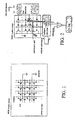
- Figure 1 shows, by way of example, the structure of a memory of the NOR type characterised in having a drain contact for each cell (in reality, due to space reasons, the contact is shared by two cells); this allows to address the single cell. The cell reading, which occurs, as said, in current, is obtained by biasing the cell and by verifying the current the same is able to absorb.
- The arrangement of the cell in the matrix array makes the current to be measured be only the one of the addressed memory cell. In this way the reading operation uses all the current available and it is thus fast. Figure 2 schematically shows this solution and also highlights the current flow.
- Instead in the case of NAND architecture, shown for example in figure 3, the matrix structure results form the stack organisation of a series of cells, typically sixteen.
- The reading of the addressed cell involves all the cells of the stack; the cell to be read is biased with a higher gate than the others of the same stack, so that these are however on while the addressed one, if virgin, will conduct current, if already programmed will not lead and thus operate as a switch to ground discriminating the information logic value,
- The presence of such a high number of cells in series, to which the contribution of the selection pass transistors is to be added, implies a reading current being of some orders of magnitude smaller than the one in the case of the NOR.
- The reading operation thus occurs with a pre-charge and test step, an integration in time which solves the problem of the measurement precision at the expense of the time necessary to perform it which is of 2-3 orders of magnitude greater than the one of the NOR case. Figure 3 schematises this situation.
- This figures shows in fact a traditional NAND structure wherein, inside the square, hereunder sixteen cells are schematically indicated forming a conventional stack of the NAND structure.
- The other fundamental difference between the NOR and the NAND architecture stays in the programming mode.
- In the NOR case the programming is obtained through the physical phenomenon of the hot electrons (CHE) while the erasing through the phenomenon known as Fowler-Nordheim tunneling.
- In the NAND case both the erasing and the programming occur through tunneling.
- The two physical phenomena have, as fundamental differences, the execution times and the current at stake.
- In the case of the hot electrons the execution times are in the order of microseconds while for the tunneling the execution times are in the order of milliseconds.
- On the contrary, the currents necessary in the case of hot electrons are in the order of tens of microAmpere while those necessary in the case of tunneling are in the order of picoAmpere and they are negligible for electronic devices.
- The result of these differences is that the writing, in the NOR case, is faster but the number of the cells which is to be programmed in parallel is at least an order of magnitude lower with respect to what can be done in the NAND case.
- To make an example: 256 cells can be programmed in parallel in a NOR memory, but as much as 4096 cells in the NAND case.
- In consequence, for memories of great size, where one can imagine that the writing operation is made of a byte only but of a lot of words together, the NAND approach is winning.
- This is why the applications increasingly converging towards a neat distinction between:
- memories for code storage: today densities around 256Mb, typical reading speed of the NOR, used exactly either as memories from which a down load operation of the code to be performed in RAM is carried out or even as execution memories, from here the need of a fast random access;
- memories for data storage, with reading density typical of the NAND, used as data memory banks, for example of photographic cards, where the fast access is not so important since there is no execution of what is downloaded by the Flash but only of an edit on the suitable support; in the case of the photograph it can be the display of a photo on a PC monitor.
- Finally, it is to be noted that the organisation of the NAND allows a simplification of the erasing operation which is more granular with respect to what is possible for the NOR.
- Having both the typologies of memories, both the ones for the data storage and those for the code storage, is normally necessary inside an electronic, system.
- Recently further new needs have arisen linked to the games and cellular phones market, which consist in having high capacity memories to store any type of datum, but also to store a video operative system, programs, results etc.
- To meet these needs the prior art has recently proposed devices defined as MCP (Multi Chip Package) which incorporate, in a single package, different integrated electronic circuits such as for example several types of memory circuits, for example one Flash memory of the NAND type, one of the NOR type and a RAM memory.
- All these memories are assembled and supplied in a single package so as to provide a single device simultaneously having the advantages of all the memories on sale, for example density and storage capability as regards the NAND portion, or access speed and XIP possibility as regards the NOR portion, random access as regards the RAM portion.
- For example, one of these devices is commercially known with the acronym OneNAND and is manufactured by the company Samsung; another example of this kind of Multi Chip Package is the "DiskOnChip" of M-System.
- Although advantageous under several aspects, and substantially meeting the aim, these devices, are not exempt from drawbacks.
- In the first place it is to be considered that the various memory circuits to be assembled in a single package are realised with different technologies, which compel to solve compatibility problems in the supplies on a single package and in the management of the input/output signals.
- In the second place, the costs of the resulting package cannot depart a lot from the overall cost of the various components, since big scale economies cannot be exploited in realising devices assembled with components being different form each other.
- The technical problem underlying the present invention is that of devising a new type of monolithically integrated electronic memory device, i.e. realised on a single chip, and having such structural and functional characteristics as to offer the same performances of a Multi Chip Package however overcoming the limits and drawbacks of that type of solution.
- The solution idea underlying the present invention is that of realising a memory integrated architecture of the NAND type and using a portion of the same to be dedicated to an architecture of the NOR or the like type, so that this memory portion shows, at least in the reading step, the performances of the NOR memories.
- On the basis of this solution idea the technical problem is solved by an electronic memory device as previously indicated and defined by
claim 1 and the following ones. - The characteristics and the advantages of the electronic memory device according to the invention will be apparent from the following description of an embodiment thereof given by way of indicative and non-limiting example with reference to the annexed drawings.
-
- Figure 1 shows a schematic view of an electronic memory device, in particular an EEPROM memory with NOR architecture realised according to the prior art;
- Figure 2 shows a further schematic view of a detail of the electronic device of figure 1 in the reading step;
- Figure 3 shows a schematic view of an electronic memory device, in particular an EEPROM memory with NAND architecture always realised according to the prior art;
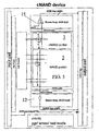
- Figure 4 shows a schematic view of an electronic memory device, in particular an EEPROM memory with cNAND architecture realised according to the present invention;
- Figure 5 shows a further schematic view of the electronic memory device of figure 4 where some paths concerning the modes of accessing data in the reading step are highlighted;
- Figure 6 shows a schematic view of a portion of an embodiment of the electronic memory device of figure 4;
- Figure 7 shows a schematic view of a portion of the electronic memory device realised according to the best embodiment of the present invention.
- With reference to these figures, and in particular to the examples of figures 4 and 6, 1 globally and schematically indicates a portion of a new electronic memory device realised according to the present invention and monolithically integrated on semiconductor as integrated circuit.
- The
device 1 is a memory of the Flash EEPROM type with architecture mainly of the NAND type. - The invention allows, at the cost of a slight modification of the array of a NAND memory, to realise, in a single chip, and thus with a single technology, a group of functions typical of different memories and up to date obtained only by means of different nature devices. In other words, the
device 1 is realised on a single chip, which integrates both the "hard disk" and boot ROM functions, avoiding resorting to the assembly of various components coming from different technologies, even if arranged on a same package. - The present invention provides the use, inside a
memory matrix 2 with NAND architecture, of aportion 3 of the same matrix to be dedicated to a NOR architecture or the like, so as to confer on thismemory portion 3 performances, in the reading step, typical of NOR memories. - More in particular, the cNAND device shown in figure 4 comprises a matrix 11 realised in NAND technology but substantially divided into two
portions portion 2 with a stack having sixteen cells and aportion 3 with a stack comprising a single cell. - Each
portion respective column decodinge relative sense amplifiers portion 3 are of the type used in the matrixes of the NOR type. - Advantageously, according to the invention, the two typologies of sense amplifiers indicated in figure 4 are the ones normally used for the NAND and NOR structures and they are mainly indicated to show the two different approaches made possible by the invention, i.e.: pre-charge and evaluation for the
NAND portion 2, continuous reading for theportion 3 of the NOR type. - A single row-decoding
portion 16 is associated both with thematrix portion 2, and with thematrix portion 3. There are then conventional circuit blocks, which compose a Flash memory, such as for example the input and output terminals and the input and output logic portions. - As shown in figure 5, the sensing operations occur with the use of a page buffer as regards the cNAND part.
- More in particular, in figure 5 it can be appreciated how the addresses drive the logic block caring for the output not of an array of the cNAND type but of a byte/word of the NOR type.
- In any case, the different access modes of the two
portions NAND portion 2 of the matrix 11. - It is to be noted that the two
portions - Moreover, another preferred characteristic is given by the fact that the memory cell structure is identical in the two
portions - The
memory portion 3 can be used for the Code Storage and it will be called cNAND (codeNAND). - Advantageously, according to the invention, to optimise the constructive process and the nowadays architecture of NAND architectures, preserving the programming and erasing structure for the
cNAND portion 3 has been provided. - In this way the connections to the decoding circuits necessary for the erasing step are not modified, to bring the matrix WELL positive and the column decoding which, in this solution, does not have to be specifically designed to bring the current necessary for the programming in the hot electrons mode.
- Moreover, the structure of the NAND matrix is not modified a lot since the drain contacts and the differentiated plants always present for the phenomenon of the hot electrons are not required.
- Figure 5 shows, in an enlargement and in greater detail, an indicative embodiment of a first possible architecture wherein the sector of NAND matrix used to obtain the
cNAND portion 3 has been reduced to asingle cell 5. - In this way, two selection transistors 4 and 6, already present in a traditional NAND structure, are maintained but the
interested cell 5 is only one. - The current this
cell 5 is able to absorb can be compared with the one of a NOR architecture and thus it is possible to realise a reading circuitry similar to the NOR onc: i.e., a circuitry being differential and in static current with all the deriving speed advantages. - The annexed table I summarises the differences between the addressed cell in a Flash sector with NOR architecture, in a sector with NAND architecture and in a sector with cNAND architecture according to the present invention.
Table 1 NAND sector NOR sector CNAND sector Program Tunnel - pA/cell CHE - mA/cell Tunnel - pA/cell Gate = 18V Gate = 10V Gate = 18V Source = 0 Source = 0 Source = 0 Drain =0 Drain =5V Drain = 0 Bulk = 0 Bulk = 0 Bulk = 0 Erase Tunnel - pA/cell Tunnel - pA/cell Tunnel - pA/cell Gate = 18V Gate = -10 Gate = 0 Source = float Source = 8V Source = float Drain = float Drain = float Drain = float Bulk = 20V Bulk = 8V Bulk = 20V Read Pre-charge/test Reading in current Reading in current Gate = 5V Gate = 5V Gate = 5V Drain = 1V Drain = 1V Drain = 1V Source = 1V-Rstack*Iread Source = 0 Source = 0 - It is obvious that a
cNAND portion 3 as the one here described is less competitive in terms of space from the point of view of the preservation of the NAND technological process. - In fact, in figure 6 it is clear how the space dedicated to the column decodes becomes preponderant with respect to the space reserved for the
memory cell 5. - A successive step to optimise the circuit area occupation is that of increasing the number of the stack cells.
- The problem of the reading speed, as already seen, is due to the presence, in the NAND case, of sixteen cells in series which constitute, during the reading step, such a high resistive step as not to make it possible the reading in current as for the NOR architectures.
- A reading has thus been preferred composed of a pre-charge and of a test, as it is done for structures of the PLA type. A typical reading with charge integration.
- Since on multilevel devices of the NOR type it is possible to distinguish different potential levels, although maintaining a reading speed lower than 100ns and using a current reference of some microAmpere, for example between 2 and 4 microAmpere, operating the reading on the
cNAND portion 3 can be hypothesised as if it were a structure of the multilevel type. - If it is hypothesised that the
cell 5 with NAND architecture has a gain of 15uA/V with a distance of 2V between the logic value "1" and the logic value "0", the difference in current between thecell 5 and a reference in current, supposed to be at half level, will be of 15uA. - In ronsequence, if one imagine that the impedance of each single cell is the same, one can think of reducing the stack of the cNAND sector to four cells with an available current exactly equal to the one already used in a NOR multilevel.
- Figure 7 schematically shows this hypothesis with definition of a
cNAND matrix portion 7 made of four rows. - To obtain the desired results in terms of reading speed, it is not enough to act only on the matrix structure, but acting also on the row decoding and on the sensing part is necessary.
- The row decoding for a NOR structure represents one of the most delicate aspects to obtain a good access speed in reading.
- If one imagine to use the solution of figure 6, with the cNAND sector made of a single cell, the row decoding to be used can be exactly the one used for a NOR structure, by using even a classic architecture since the only thing to do is that of bringing, on the gate terminal of the
cell 5, a positive voltage, both in the reading and in the writing step. - Therefore, it is not necessary to use possible decoding structures of modem generation, which allow bringing, on the gate terminal, also negative voltages.
- This represents an advantage since the same manufacturing process structure is to be maintained, and thus the same NAND memories programming and crasing modes as well.
- Instead, in case a minimum stack is to be maintained, as the one of figure 7, the row decoding must be realised like the one of a NOR structure wherein the non selected rows must be however brought to a positive value during the reading step, as realised for a classic NAND architecture.
- As regards the sensing circuitry, which is fundamental for the speed in reading, must be realised like for the NOR structures, i.e. so that the cNAND sector portions are placed on the same side (with respect to the bit-lines) of the matrix and so that the bit-line connection can go out from the matrix area and there is the same space to place the necessary sense amplifiers and the rauting.
- The output of the sense amplifiers dedicated to the cNAND sectors must converge with the outputs of the NAND senses to reach common outputs.
- The output circuitry has been modified as shown in figure 5 to obtain a Random access to the cNAND sectors.
- As already seen, always with reference to the example of figure 5, each
portion relative sense amplifiers portion 3 are of the type used in the matrixes of the NOR type. - The invention thus makes two different approaches possible: pre-charge and test for the
NAND portion 2, continuous reading for theportion 3 of the NOR type. - The logic is realised so that, once the address inside the cNAND sectors is known, the Random access is automatic and, after an access time successive to the presentation of the addresses, data can be obtained on the outputs.
- The invention thus solves the technical problem and attains several advantages, the first one of which is surely given by the fact that in a single integrated circuit memory portions are housed having data storage capacity and relative data access speeds, but realised with the same technology.
- The invention can be easily implemented since the construction of the matrix does not change for the
NAND portion 2 and for thecNAND portion 3; only the number of the components of the respective stacks of cells changes.
Claims (10)
- Non volatile electronic memory device (1) being monolithically integrated on semiconductor and of the Flash EEPROM having NAND architecture and comprising at least one memory matrix (11) organised in rows and columns of memory cells, wherein said matrix (11) comprises at least one portion (3) having different data storage capacity and different access speed with respect to the remaining matrix portion (2).
- Device according to claim 1, characterised in that said portion (3) is of the NOR type or the like.
- Device according to claim 1, characterised in that the reading step of said portion (3) is a current reading.
- Device according to claim 1, characterised in that said portion (3) comprises one stack of cells with a single cell (5).
- Device according to claim 1, characterised in that said portion (3) comprises one stack of cells with only four cells (5).
- Device according to claim 1, characterised in that said portion (3) is associated with a row decoding circuitry having sense amplifiers of the NOR type.
- Device according to claim 1, characterised in that said remaining matrix portion (2) has a structure of the NAND type.
- Device according to claim 7, characterised in that the number of cells in said portion (3) and in said remaining portion (2) is different.
- Device according to claim 3, characterised in that said portion (3) has a random access mode.
- Device according to claim 1, characterised in that the cells of the remaining portion (2) of memory matrix (11) are read by means of a first pre-charge step and a successive test step.
Applications Claiming Priority (1)
| Application Number | Priority Date | Filing Date | Title |
|---|---|---|---|
| IT000608A ITMI20050608A1 (en) | 2005-04-11 | 2005-04-11 | ELECTRONIC DEVICE OF NON-VOLATILE MEMORY WITH CNAND STRUCTURE INTEGRATED MONOLITHICALLY ON SEMICONDUCTOR |
Publications (1)
| Publication Number | Publication Date |
|---|---|
| EP1713081A1 true EP1713081A1 (en) | 2006-10-18 |
Family
ID=36754314
Family Applications (1)
| Application Number | Title | Priority Date | Filing Date |
|---|---|---|---|
| EP06007497A Withdrawn EP1713081A1 (en) | 2005-04-11 | 2006-04-10 | Electronic non-volatile memory device having a "code NAND" structure and being monolithically integrated on a semiconductor substrate |
Country Status (3)
| Country | Link |
|---|---|
| US (1) | US7675788B2 (en) |
| EP (1) | EP1713081A1 (en) |
| IT (1) | ITMI20050608A1 (en) |
Families Citing this family (2)
| Publication number | Priority date | Publication date | Assignee | Title |
|---|---|---|---|---|
| US8320191B2 (en) | 2007-08-30 | 2012-11-27 | Infineon Technologies Ag | Memory cell arrangement, method for controlling a memory cell, memory array and electronic device |
| WO2021232259A1 (en) | 2020-05-20 | 2021-11-25 | Yangtze Memory Technologies Co., Ltd. | 3d nand flash memory device and integration method thereof |
Citations (6)
| Publication number | Priority date | Publication date | Assignee | Title |
|---|---|---|---|---|
| US5553016A (en) * | 1992-03-26 | 1996-09-03 | Kabushiki Kaisha Toshiba | Semiconductor memory device |
| US5777925A (en) * | 1996-07-11 | 1998-07-07 | Kabushiki Kaisha Toshiba | Semiconductor non-volatile memory device |
| US6032248A (en) * | 1998-04-29 | 2000-02-29 | Atmel Corporation | Microcontroller including a single memory module having a data memory sector and a code memory sector and supporting simultaneous read/write access to both sectors |
| US20020186591A1 (en) * | 2001-06-11 | 2002-12-12 | Sumsung Electronics Co,. Ltd. | Semiconductor memory device having memory cell arrays capable of accomplishing random access |
| US20030128584A1 (en) * | 2002-01-07 | 2003-07-10 | Mitsubishi Denki Kabushiki Kaisha | Non-volatile semiconductor memory device |
| US20040238880A1 (en) * | 2003-05-30 | 2004-12-02 | Shigeru Nagasaka | Nonvolatile semiconductor memory device including MOS transistors each having a floating gate and control gate |
Family Cites Families (5)
| Publication number | Priority date | Publication date | Assignee | Title |
|---|---|---|---|---|
| JP3999900B2 (en) * | 1998-09-10 | 2007-10-31 | 株式会社東芝 | Nonvolatile semiconductor memory |
| US6175523B1 (en) * | 1999-10-25 | 2001-01-16 | Advanced Micro Devices, Inc | Precharging mechanism and method for NAND-based flash memory devices |
| JP2004326864A (en) * | 2003-04-22 | 2004-11-18 | Toshiba Corp | Non-volatile semiconductor memory |
| US7274594B2 (en) * | 2005-04-11 | 2007-09-25 | Stmicroelectronics S.R.L. | Non-volatile memory electronic device with NAND structure being monolithically integrated on semiconductor |
| ITRM20050353A1 (en) * | 2005-07-04 | 2007-01-05 | Micron Technology Inc | DETECTOR LOW POWER HIGHER DETECTION AMPLIFIER. |
-
2005
- 2005-04-11 IT IT000608A patent/ITMI20050608A1/en unknown
-
2006
- 2006-04-10 EP EP06007497A patent/EP1713081A1/en not_active Withdrawn
- 2006-04-11 US US11/401,521 patent/US7675788B2/en active Active
Patent Citations (6)
| Publication number | Priority date | Publication date | Assignee | Title |
|---|---|---|---|---|
| US5553016A (en) * | 1992-03-26 | 1996-09-03 | Kabushiki Kaisha Toshiba | Semiconductor memory device |
| US5777925A (en) * | 1996-07-11 | 1998-07-07 | Kabushiki Kaisha Toshiba | Semiconductor non-volatile memory device |
| US6032248A (en) * | 1998-04-29 | 2000-02-29 | Atmel Corporation | Microcontroller including a single memory module having a data memory sector and a code memory sector and supporting simultaneous read/write access to both sectors |
| US20020186591A1 (en) * | 2001-06-11 | 2002-12-12 | Sumsung Electronics Co,. Ltd. | Semiconductor memory device having memory cell arrays capable of accomplishing random access |
| US20030128584A1 (en) * | 2002-01-07 | 2003-07-10 | Mitsubishi Denki Kabushiki Kaisha | Non-volatile semiconductor memory device |
| US20040238880A1 (en) * | 2003-05-30 | 2004-12-02 | Shigeru Nagasaka | Nonvolatile semiconductor memory device including MOS transistors each having a floating gate and control gate |
Also Published As
| Publication number | Publication date |
|---|---|
| US20060250847A1 (en) | 2006-11-09 |
| US7675788B2 (en) | 2010-03-09 |
| ITMI20050608A1 (en) | 2006-10-12 |
Similar Documents
| Publication | Publication Date | Title |
|---|---|---|
| US6525969B1 (en) | Decoder apparatus and methods for pre-charging bit lines | |
| US6510082B1 (en) | Drain side sensing scheme for virtual ground flash EPROM array with adjacent bit charge and hold | |
| US6954382B2 (en) | Multiple use memory chip | |
| KR100323970B1 (en) | Non-volatile memory structure | |
| US6529412B1 (en) | Source side sensing scheme for virtual ground read of flash eprom array with adjacent bit precharge | |
| JP7132443B2 (en) | METHOD OF PROGRAMMING MEMORY DEVICES, SYSTEMS AND RELATED MEMORY DEVICES | |
| NZ522383A (en) | Electrically-eraseable programmable read-only memory having reduced-page-size program and erase | |
| US20100177568A1 (en) | Read mode for flash memory | |
| US20030235066A1 (en) | Ferroelectric write once read only memory for archival storage | |
| JP2006114137A (en) | Semiconductor memory device | |
| KR20070010160A (en) | Methods and systems for high performance write in multi-bit flash memory devices | |
| US5067111A (en) | Semiconductor memory device having a majority logic for determining data to be read out | |
| CN116825165B (en) | Grid-splitter memory array and its operation method | |
| US7366027B2 (en) | Method and apparatus for erasing memory | |
| JPH1027484A (en) | Semiconductor nonvolatile storage device | |
| JP2007294109A (en) | Memory element and data read-out method | |
| US6549473B2 (en) | Circuital structure for reading data in a non-volatile memory device | |
| US7675788B2 (en) | Electronic non-volatile memory device having a cNAND structure and being monolithically integrated on semiconductor | |
| US12538498B2 (en) | Memory device implementing unified memory architecture integrating multiple memory types | |
| CN116884458A (en) | Split-gate memory array and method of operating the same | |
| US6970368B1 (en) | CAM (content addressable memory) cells as part of core array in flash memory device | |
| JP3827953B2 (en) | Nonvolatile semiconductor memory device | |
| CN1494086A (en) | Bimetal oxide-nitride-oxide semiconductor array metal position structure and single unit operation | |
| JP3197858B2 (en) | Semiconductor memory device | |
| JPH08204036A (en) | Nonvolatile semiconductor memory device |
Legal Events
| Date | Code | Title | Description |
|---|---|---|---|
| PUAI | Public reference made under article 153(3) epc to a published international application that has entered the european phase |
Free format text: ORIGINAL CODE: 0009012 |
|
| AK | Designated contracting states |
Kind code of ref document: A1 Designated state(s): AT BE BG CH CY CZ DE DK EE ES FI FR GB GR HU IE IS IT LI LT LU LV MC NL PL PT RO SE SI SK TR |
|
| AX | Request for extension of the european patent |
Extension state: AL BA HR MK YU |
|
| AKX | Designation fees paid | ||
| REG | Reference to a national code |
Ref country code: DE Ref legal event code: 8566 |
|
| STAA | Information on the status of an ep patent application or granted ep patent |
Free format text: STATUS: THE APPLICATION IS DEEMED TO BE WITHDRAWN |
|
| 18D | Application deemed to be withdrawn |
Effective date: 20070419 |