EP1712298A1 - Organic thin film insulator - Google Patents
Organic thin film insulator Download PDFInfo
- Publication number
- EP1712298A1 EP1712298A1 EP05008047A EP05008047A EP1712298A1 EP 1712298 A1 EP1712298 A1 EP 1712298A1 EP 05008047 A EP05008047 A EP 05008047A EP 05008047 A EP05008047 A EP 05008047A EP 1712298 A1 EP1712298 A1 EP 1712298A1
- Authority
- EP
- European Patent Office
- Prior art keywords
- layer
- layer system
- substrate
- monolayer
- thin film
- Prior art date
- Legal status (The legal status is an assumption and is not a legal conclusion. Google has not performed a legal analysis and makes no representation as to the accuracy of the status listed.)
- Granted
Links
- 239000010409 thin film Substances 0.000 title claims abstract description 13
- 239000012212 insulator Substances 0.000 title description 10
- 239000010410 layer Substances 0.000 claims abstract description 76
- 239000000758 substrate Substances 0.000 claims abstract description 45
- 239000002356 single layer Substances 0.000 claims abstract description 23
- 230000005294 ferromagnetic effect Effects 0.000 claims abstract description 12
- 230000005291 magnetic effect Effects 0.000 claims abstract description 7
- 239000004065 semiconductor Substances 0.000 claims abstract description 7
- 238000004377 microelectronic Methods 0.000 claims abstract description 6
- PXHVJJICTQNCMI-UHFFFAOYSA-N Nickel Chemical compound [Ni] PXHVJJICTQNCMI-UHFFFAOYSA-N 0.000 claims description 61
- 239000010931 gold Substances 0.000 claims description 38
- 239000010408 film Substances 0.000 claims description 37
- 239000013545 self-assembled monolayer Substances 0.000 claims description 34
- 229910052751 metal Inorganic materials 0.000 claims description 21
- 239000002184 metal Substances 0.000 claims description 21
- 229910052737 gold Inorganic materials 0.000 claims description 16
- XEEYBQQBJWHFJM-UHFFFAOYSA-N Iron Chemical compound [Fe] XEEYBQQBJWHFJM-UHFFFAOYSA-N 0.000 claims description 14
- 229910052759 nickel Inorganic materials 0.000 claims description 13
- 125000000524 functional group Chemical group 0.000 claims description 9
- PCHJSUWPFVWCPO-UHFFFAOYSA-N gold Chemical compound [Au] PCHJSUWPFVWCPO-UHFFFAOYSA-N 0.000 claims description 9
- 125000003118 aryl group Chemical group 0.000 claims description 8
- 125000001072 heteroaryl group Chemical group 0.000 claims description 7
- 229910052742 iron Inorganic materials 0.000 claims description 7
- MWPLVEDNUUSJAV-UHFFFAOYSA-N anthracene Chemical compound C1=CC=CC2=CC3=CC=CC=C3C=C21 MWPLVEDNUUSJAV-UHFFFAOYSA-N 0.000 claims description 6
- 229910017052 cobalt Inorganic materials 0.000 claims description 6
- 239000010941 cobalt Substances 0.000 claims description 6
- GUTLYIVDDKVIGB-UHFFFAOYSA-N cobalt atom Chemical compound [Co] GUTLYIVDDKVIGB-UHFFFAOYSA-N 0.000 claims description 6
- RYGMFSIKBFXOCR-UHFFFAOYSA-N Copper Chemical compound [Cu] RYGMFSIKBFXOCR-UHFFFAOYSA-N 0.000 claims description 4
- UFWIBTONFRDIAS-UHFFFAOYSA-N Naphthalene Chemical compound C1=CC=CC2=CC=CC=C21 UFWIBTONFRDIAS-UHFFFAOYSA-N 0.000 claims description 4
- KAESVJOAVNADME-UHFFFAOYSA-N Pyrrole Chemical compound C=1C=CNC=1 KAESVJOAVNADME-UHFFFAOYSA-N 0.000 claims description 4
- BQCADISMDOOEFD-UHFFFAOYSA-N Silver Chemical compound [Ag] BQCADISMDOOEFD-UHFFFAOYSA-N 0.000 claims description 4
- 229910052782 aluminium Inorganic materials 0.000 claims description 4
- XAGFODPZIPBFFR-UHFFFAOYSA-N aluminium Chemical compound [Al] XAGFODPZIPBFFR-UHFFFAOYSA-N 0.000 claims description 4
- 229910052802 copper Inorganic materials 0.000 claims description 4
- 239000010949 copper Substances 0.000 claims description 4
- ZUOUZKKEUPVFJK-UHFFFAOYSA-N diphenyl Chemical compound C1=CC=CC=C1C1=CC=CC=C1 ZUOUZKKEUPVFJK-UHFFFAOYSA-N 0.000 claims description 4
- 150000002739 metals Chemical class 0.000 claims description 4
- 229910052709 silver Inorganic materials 0.000 claims description 4
- 239000004332 silver Substances 0.000 claims description 4
- YJTKZCDBKVTVBY-UHFFFAOYSA-N 1,3-Diphenylbenzene Chemical group C1=CC=CC=C1C1=CC=CC(C=2C=CC=CC=2)=C1 YJTKZCDBKVTVBY-UHFFFAOYSA-N 0.000 claims description 3
- YTPLMLYBLZKORZ-UHFFFAOYSA-N Thiophene Chemical compound C=1C=CSC=1 YTPLMLYBLZKORZ-UHFFFAOYSA-N 0.000 claims description 3
- 239000004411 aluminium Substances 0.000 claims description 3
- 125000003178 carboxy group Chemical group [H]OC(*)=O 0.000 claims description 3
- 239000002094 self assembled monolayer Substances 0.000 claims description 3
- 238000009281 ultraviolet germicidal irradiation Methods 0.000 claims description 3
- 235000010290 biphenyl Nutrition 0.000 claims description 2
- 239000004305 biphenyl Substances 0.000 claims description 2
- 125000001997 phenyl group Chemical group [H]C1=C([H])C([H])=C(*)C([H])=C1[H] 0.000 claims description 2
- KDLHZDBZIXYQEI-UHFFFAOYSA-N Palladium Chemical compound [Pd] KDLHZDBZIXYQEI-UHFFFAOYSA-N 0.000 claims 2
- JUJWROOIHBZHMG-UHFFFAOYSA-N Pyridine Chemical compound C1=CC=NC=C1 JUJWROOIHBZHMG-UHFFFAOYSA-N 0.000 claims 1
- 125000001160 methoxycarbonyl group Chemical group [H]C([H])([H])OC(*)=O 0.000 claims 1
- 239000012044 organic layer Substances 0.000 claims 1
- 229910052763 palladium Inorganic materials 0.000 claims 1
- 238000009413 insulation Methods 0.000 abstract description 4
- 238000001228 spectrum Methods 0.000 description 12
- XOJVVFBFDXDTEG-UHFFFAOYSA-N Norphytane Natural products CC(C)CCCC(C)CCCC(C)CCCC(C)C XOJVVFBFDXDTEG-UHFFFAOYSA-N 0.000 description 10
- 238000000034 method Methods 0.000 description 10
- 238000004132 cross linking Methods 0.000 description 9
- 238000001704 evaporation Methods 0.000 description 9
- 230000008020 evaporation Effects 0.000 description 9
- 239000000470 constituent Substances 0.000 description 8
- 238000002848 electrochemical method Methods 0.000 description 7
- XKRFYHLGVUSROY-UHFFFAOYSA-N Argon Chemical compound [Ar] XKRFYHLGVUSROY-UHFFFAOYSA-N 0.000 description 6
- 238000004833 X-ray photoelectron spectroscopy Methods 0.000 description 6
- 230000015572 biosynthetic process Effects 0.000 description 6
- 238000009792 diffusion process Methods 0.000 description 6
- 238000005259 measurement Methods 0.000 description 6
- 238000004998 X ray absorption near edge structure spectroscopy Methods 0.000 description 5
- 150000001875 compounds Chemical class 0.000 description 5
- 238000000151 deposition Methods 0.000 description 5
- 230000008021 deposition Effects 0.000 description 5
- 238000002474 experimental method Methods 0.000 description 5
- 238000004519 manufacturing process Methods 0.000 description 5
- 239000000463 material Substances 0.000 description 5
- OKTJSMMVPCPJKN-UHFFFAOYSA-N Carbon Chemical compound [C] OKTJSMMVPCPJKN-UHFFFAOYSA-N 0.000 description 4
- XUIMIQQOPSSXEZ-UHFFFAOYSA-N Silicon Chemical compound [Si] XUIMIQQOPSSXEZ-UHFFFAOYSA-N 0.000 description 4
- 230000003628 erosive effect Effects 0.000 description 4
- 239000007789 gas Substances 0.000 description 4
- 238000001566 impedance spectroscopy Methods 0.000 description 4
- 150000002500 ions Chemical class 0.000 description 4
- 230000035515 penetration Effects 0.000 description 4
- 239000000523 sample Substances 0.000 description 4
- 229910052710 silicon Inorganic materials 0.000 description 4
- 239000010703 silicon Substances 0.000 description 4
- 238000001179 sorption measurement Methods 0.000 description 4
- 239000000126 substance Substances 0.000 description 4
- 150000003573 thiols Chemical class 0.000 description 4
- 101000799388 Homo sapiens Thiopurine S-methyltransferase Proteins 0.000 description 3
- 102100034162 Thiopurine S-methyltransferase Human genes 0.000 description 3
- 239000002156 adsorbate Substances 0.000 description 3
- 229910052786 argon Inorganic materials 0.000 description 3
- 229910052799 carbon Inorganic materials 0.000 description 3
- 230000007423 decrease Effects 0.000 description 3
- 238000007654 immersion Methods 0.000 description 3
- 125000000449 nitro group Chemical group [O-][N+](*)=O 0.000 description 3
- 230000002688 persistence Effects 0.000 description 3
- BASFCYQUMIYNBI-UHFFFAOYSA-N platinum Chemical compound [Pt] BASFCYQUMIYNBI-UHFFFAOYSA-N 0.000 description 3
- 230000005855 radiation Effects 0.000 description 3
- 125000006850 spacer group Chemical group 0.000 description 3
- 230000001052 transient effect Effects 0.000 description 3
- NEAQRZUHTPSBBM-UHFFFAOYSA-N 2-hydroxy-3,3-dimethyl-7-nitro-4h-isoquinolin-1-one Chemical compound C1=C([N+]([O-])=O)C=C2C(=O)N(O)C(C)(C)CC2=C1 NEAQRZUHTPSBBM-UHFFFAOYSA-N 0.000 description 2
- 229910052581 Si3N4 Inorganic materials 0.000 description 2
- VYPSYNLAJGMNEJ-UHFFFAOYSA-N Silicium dioxide Chemical compound O=[Si]=O VYPSYNLAJGMNEJ-UHFFFAOYSA-N 0.000 description 2
- 238000010521 absorption reaction Methods 0.000 description 2
- 239000000956 alloy Substances 0.000 description 2
- 229910045601 alloy Inorganic materials 0.000 description 2
- 238000004458 analytical method Methods 0.000 description 2
- 238000004873 anchoring Methods 0.000 description 2
- 150000001491 aromatic compounds Chemical class 0.000 description 2
- 230000006399 behavior Effects 0.000 description 2
- 238000002484 cyclic voltammetry Methods 0.000 description 2
- 238000009826 distribution Methods 0.000 description 2
- 239000003792 electrolyte Substances 0.000 description 2
- 239000008151 electrolyte solution Substances 0.000 description 2
- 238000000572 ellipsometry Methods 0.000 description 2
- 230000005669 field effect Effects 0.000 description 2
- 230000006870 function Effects 0.000 description 2
- 238000007306 functionalization reaction Methods 0.000 description 2
- 150000002390 heteroarenes Chemical class 0.000 description 2
- 238000001453 impedance spectrum Methods 0.000 description 2
- 238000010884 ion-beam technique Methods 0.000 description 2
- 238000002360 preparation method Methods 0.000 description 2
- 230000008569 process Effects 0.000 description 2
- 230000002829 reductive effect Effects 0.000 description 2
- 125000002327 selenol group Chemical class [H][Se]* 0.000 description 2
- HQVNEWCFYHHQES-UHFFFAOYSA-N silicon nitride Chemical compound N12[Si]34N5[Si]62N3[Si]51N64 HQVNEWCFYHHQES-UHFFFAOYSA-N 0.000 description 2
- OHLFVTCARHBZDH-UHFFFAOYSA-N 1,4-dicyclohexylcyclohexane Chemical group C1CCCCC1C1CCC(C2CCCCC2)CC1 OHLFVTCARHBZDH-UHFFFAOYSA-N 0.000 description 1
- JFJNVIPVOCESGZ-UHFFFAOYSA-N 2,3-dipyridin-2-ylpyridine Chemical compound N1=CC=CC=C1C1=CC=CN=C1C1=CC=CC=N1 JFJNVIPVOCESGZ-UHFFFAOYSA-N 0.000 description 1
- JBRZTFJDHDCESZ-UHFFFAOYSA-N AsGa Chemical compound [As]#[Ga] JBRZTFJDHDCESZ-UHFFFAOYSA-N 0.000 description 1
- 229910001020 Au alloy Inorganic materials 0.000 description 1
- ROFVEXUMMXZLPA-UHFFFAOYSA-N Bipyridyl Chemical compound N1=CC=CC=C1C1=CC=CC=N1 ROFVEXUMMXZLPA-UHFFFAOYSA-N 0.000 description 1
- 241000819038 Chichester Species 0.000 description 1
- VYZAMTAEIAYCRO-UHFFFAOYSA-N Chromium Chemical compound [Cr] VYZAMTAEIAYCRO-UHFFFAOYSA-N 0.000 description 1
- 101100425892 Danio rerio tpma gene Proteins 0.000 description 1
- 229910001218 Gallium arsenide Inorganic materials 0.000 description 1
- 238000004566 IR spectroscopy Methods 0.000 description 1
- 229910021607 Silver chloride Inorganic materials 0.000 description 1
- 101150048952 TPM-1 gene Proteins 0.000 description 1
- RTAQQCXQSZGOHL-UHFFFAOYSA-N Titanium Chemical compound [Ti] RTAQQCXQSZGOHL-UHFFFAOYSA-N 0.000 description 1
- XFHIDPOTWOFDEM-UHFFFAOYSA-N [4-[4-(sulfanylmethyl)phenyl]phenyl]methanethiol Chemical compound C1=CC(CS)=CC=C1C1=CC=C(CS)C=C1 XFHIDPOTWOFDEM-UHFFFAOYSA-N 0.000 description 1
- 239000002253 acid Substances 0.000 description 1
- 125000003158 alcohol group Chemical group 0.000 description 1
- PNEYBMLMFCGWSK-UHFFFAOYSA-N aluminium oxide Inorganic materials [O-2].[O-2].[O-2].[Al+3].[Al+3] PNEYBMLMFCGWSK-UHFFFAOYSA-N 0.000 description 1
- 125000003277 amino group Chemical group 0.000 description 1
- 238000013459 approach Methods 0.000 description 1
- 239000007864 aqueous solution Substances 0.000 description 1
- 238000004630 atomic force microscopy Methods 0.000 description 1
- QVGXLLKOCUKJST-UHFFFAOYSA-N atomic oxygen Chemical compound [O] QVGXLLKOCUKJST-UHFFFAOYSA-N 0.000 description 1
- 230000004888 barrier function Effects 0.000 description 1
- 230000005587 bubbling Effects 0.000 description 1
- 150000001735 carboxylic acids Chemical class 0.000 description 1
- 230000015556 catabolic process Effects 0.000 description 1
- 229910052804 chromium Inorganic materials 0.000 description 1
- 239000011651 chromium Substances 0.000 description 1
- 229910052681 coesite Inorganic materials 0.000 description 1
- 238000001816 cooling Methods 0.000 description 1
- 229910052593 corundum Inorganic materials 0.000 description 1
- 230000008878 coupling Effects 0.000 description 1
- 238000010168 coupling process Methods 0.000 description 1
- 238000005859 coupling reaction Methods 0.000 description 1
- 229910052906 cristobalite Inorganic materials 0.000 description 1
- 125000000113 cyclohexyl group Chemical group [H]C1([H])C([H])([H])C([H])([H])C([H])(*)C([H])([H])C1([H])[H] 0.000 description 1
- WVIIMZNLDWSIRH-UHFFFAOYSA-N cyclohexylcyclohexane Chemical group C1CCCCC1C1CCCCC1 WVIIMZNLDWSIRH-UHFFFAOYSA-N 0.000 description 1
- 239000007857 degradation product Substances 0.000 description 1
- 238000006731 degradation reaction Methods 0.000 description 1
- 238000006356 dehydrogenation reaction Methods 0.000 description 1
- 239000003989 dielectric material Substances 0.000 description 1
- 230000005684 electric field Effects 0.000 description 1
- 238000010292 electrical insulation Methods 0.000 description 1
- 230000005670 electromagnetic radiation Effects 0.000 description 1
- 238000011066 ex-situ storage Methods 0.000 description 1
- 230000004907 flux Effects 0.000 description 1
- 229910052732 germanium Inorganic materials 0.000 description 1
- GNPVGFCGXDBREM-UHFFFAOYSA-N germanium atom Chemical compound [Ge] GNPVGFCGXDBREM-UHFFFAOYSA-N 0.000 description 1
- 239000010439 graphite Substances 0.000 description 1
- 229910002804 graphite Inorganic materials 0.000 description 1
- 238000002272 high-resolution X-ray photoelectron spectroscopy Methods 0.000 description 1
- 238000002847 impedance measurement Methods 0.000 description 1
- 239000012535 impurity Substances 0.000 description 1
- 238000011065 in-situ storage Methods 0.000 description 1
- AMGQUBHHOARCQH-UHFFFAOYSA-N indium;oxotin Chemical compound [In].[Sn]=O AMGQUBHHOARCQH-UHFFFAOYSA-N 0.000 description 1
- 238000002129 infrared reflectance spectroscopy Methods 0.000 description 1
- 230000001678 irradiating effect Effects 0.000 description 1
- 238000002267 linear dichroism spectroscopy Methods 0.000 description 1
- 125000005647 linker group Chemical group 0.000 description 1
- 238000001819 mass spectrum Methods 0.000 description 1
- 230000001404 mediated effect Effects 0.000 description 1
- QSHDDOUJBYECFT-UHFFFAOYSA-N mercury Chemical compound [Hg] QSHDDOUJBYECFT-UHFFFAOYSA-N 0.000 description 1
- 229910052753 mercury Inorganic materials 0.000 description 1
- -1 metallic Substances 0.000 description 1
- 125000001570 methylene group Chemical group [H]C([H])([*:1])[*:2] 0.000 description 1
- 230000005012 migration Effects 0.000 description 1
- 238000013508 migration Methods 0.000 description 1
- 239000000203 mixture Substances 0.000 description 1
- 230000004048 modification Effects 0.000 description 1
- 238000012986 modification Methods 0.000 description 1
- 238000004776 molecular orbital Methods 0.000 description 1
- 150000002790 naphthalenes Chemical class 0.000 description 1
- 230000006911 nucleation Effects 0.000 description 1
- 238000010899 nucleation Methods 0.000 description 1
- 239000013307 optical fiber Substances 0.000 description 1
- 238000010525 oxidative degradation reaction Methods 0.000 description 1
- 239000001301 oxygen Substances 0.000 description 1
- 229910052760 oxygen Inorganic materials 0.000 description 1
- 238000012856 packing Methods 0.000 description 1
- 230000036961 partial effect Effects 0.000 description 1
- SLIUAWYAILUBJU-UHFFFAOYSA-N pentacene Chemical compound C1=CC=CC2=CC3=CC4=CC5=CC=CC=C5C=C4C=C3C=C21 SLIUAWYAILUBJU-UHFFFAOYSA-N 0.000 description 1
- VLTRZXGMWDSKGL-UHFFFAOYSA-N perchloric acid Chemical compound OCl(=O)(=O)=O VLTRZXGMWDSKGL-UHFFFAOYSA-N 0.000 description 1
- 125000002467 phosphate group Chemical group [H]OP(=O)(O[H])O[*] 0.000 description 1
- UEZVMMHDMIWARA-UHFFFAOYSA-M phosphonate Chemical compound [O-]P(=O)=O UEZVMMHDMIWARA-UHFFFAOYSA-M 0.000 description 1
- 150000003009 phosphonic acids Chemical group 0.000 description 1
- 230000001443 photoexcitation Effects 0.000 description 1
- 229910052697 platinum Inorganic materials 0.000 description 1
- 230000010287 polarization Effects 0.000 description 1
- 238000003380 quartz crystal microbalance Methods 0.000 description 1
- 230000009257 reactivity Effects 0.000 description 1
- 230000000979 retarding effect Effects 0.000 description 1
- 238000001338 self-assembly Methods 0.000 description 1
- 150000003376 silicon Chemical class 0.000 description 1
- 239000000377 silicon dioxide Substances 0.000 description 1
- HKZLPVFGJNLROG-UHFFFAOYSA-M silver monochloride Chemical compound [Cl-].[Ag+] HKZLPVFGJNLROG-UHFFFAOYSA-M 0.000 description 1
- 239000000243 solution Substances 0.000 description 1
- 239000002904 solvent Substances 0.000 description 1
- 230000003068 static effect Effects 0.000 description 1
- 229910052682 stishovite Inorganic materials 0.000 description 1
- 238000003860 storage Methods 0.000 description 1
- 230000007847 structural defect Effects 0.000 description 1
- 230000001629 suppression Effects 0.000 description 1
- 238000005211 surface analysis Methods 0.000 description 1
- 230000003746 surface roughness Effects 0.000 description 1
- 238000002207 thermal evaporation Methods 0.000 description 1
- 125000003396 thiol group Chemical group [H]S* 0.000 description 1
- 150000007944 thiolates Chemical class 0.000 description 1
- 229930192474 thiophene Natural products 0.000 description 1
- 239000010936 titanium Substances 0.000 description 1
- 229910052719 titanium Inorganic materials 0.000 description 1
- 125000005369 trialkoxysilyl group Chemical group 0.000 description 1
- ZDHXKXAHOVTTAH-UHFFFAOYSA-N trichlorosilane Chemical class Cl[SiH](Cl)Cl ZDHXKXAHOVTTAH-UHFFFAOYSA-N 0.000 description 1
- PPDADIYYMSXQJK-UHFFFAOYSA-N trichlorosilicon Chemical group Cl[Si](Cl)Cl PPDADIYYMSXQJK-UHFFFAOYSA-N 0.000 description 1
- 229910052905 tridymite Inorganic materials 0.000 description 1
- QQQSFSZALRVCSZ-UHFFFAOYSA-N triethoxysilane Chemical compound CCO[SiH](OCC)OCC QQQSFSZALRVCSZ-UHFFFAOYSA-N 0.000 description 1
- YUYCVXFAYWRXLS-UHFFFAOYSA-N trimethoxysilane Chemical compound CO[SiH](OC)OC YUYCVXFAYWRXLS-UHFFFAOYSA-N 0.000 description 1
- 235000012431 wafers Nutrition 0.000 description 1
- 229910001845 yogo sapphire Inorganic materials 0.000 description 1
Images


Classifications
-
- H—ELECTRICITY
- H10—SEMICONDUCTOR DEVICES; ELECTRIC SOLID-STATE DEVICES NOT OTHERWISE PROVIDED FOR
- H10N—ELECTRIC SOLID-STATE DEVICES NOT OTHERWISE PROVIDED FOR
- H10N50/00—Galvanomagnetic devices
- H10N50/80—Constructional details
- H10N50/85—Materials of the active region
-
- B—PERFORMING OPERATIONS; TRANSPORTING
- B05—SPRAYING OR ATOMISING IN GENERAL; APPLYING FLUENT MATERIALS TO SURFACES, IN GENERAL
- B05D—PROCESSES FOR APPLYING FLUENT MATERIALS TO SURFACES, IN GENERAL
- B05D1/00—Processes for applying liquids or other fluent materials
- B05D1/18—Processes for applying liquids or other fluent materials performed by dipping
- B05D1/185—Processes for applying liquids or other fluent materials performed by dipping applying monomolecular layers
-
- B—PERFORMING OPERATIONS; TRANSPORTING
- B82—NANOTECHNOLOGY
- B82Y—SPECIFIC USES OR APPLICATIONS OF NANOSTRUCTURES; MEASUREMENT OR ANALYSIS OF NANOSTRUCTURES; MANUFACTURE OR TREATMENT OF NANOSTRUCTURES
- B82Y10/00—Nanotechnology for information processing, storage or transmission, e.g. quantum computing or single electron logic
-
- B—PERFORMING OPERATIONS; TRANSPORTING
- B82—NANOTECHNOLOGY
- B82Y—SPECIFIC USES OR APPLICATIONS OF NANOSTRUCTURES; MEASUREMENT OR ANALYSIS OF NANOSTRUCTURES; MANUFACTURE OR TREATMENT OF NANOSTRUCTURES
- B82Y30/00—Nanotechnology for materials or surface science, e.g. nanocomposites
-
- B—PERFORMING OPERATIONS; TRANSPORTING
- B82—NANOTECHNOLOGY
- B82Y—SPECIFIC USES OR APPLICATIONS OF NANOSTRUCTURES; MEASUREMENT OR ANALYSIS OF NANOSTRUCTURES; MANUFACTURE OR TREATMENT OF NANOSTRUCTURES
- B82Y40/00—Manufacture or treatment of nanostructures
-
- B—PERFORMING OPERATIONS; TRANSPORTING
- B05—SPRAYING OR ATOMISING IN GENERAL; APPLYING FLUENT MATERIALS TO SURFACES, IN GENERAL
- B05D—PROCESSES FOR APPLYING FLUENT MATERIALS TO SURFACES, IN GENERAL
- B05D3/00—Pretreatment of surfaces to which liquids or other fluent materials are to be applied; After-treatment of applied coatings, e.g. intermediate treating of an applied coating preparatory to subsequent applications of liquids or other fluent materials
- B05D3/06—Pretreatment of surfaces to which liquids or other fluent materials are to be applied; After-treatment of applied coatings, e.g. intermediate treating of an applied coating preparatory to subsequent applications of liquids or other fluent materials by exposure to radiation
- B05D3/061—Pretreatment of surfaces to which liquids or other fluent materials are to be applied; After-treatment of applied coatings, e.g. intermediate treating of an applied coating preparatory to subsequent applications of liquids or other fluent materials by exposure to radiation using U.V.
- B05D3/065—After-treatment
- B05D3/067—Curing or cross-linking the coating
-
- B—PERFORMING OPERATIONS; TRANSPORTING
- B05—SPRAYING OR ATOMISING IN GENERAL; APPLYING FLUENT MATERIALS TO SURFACES, IN GENERAL
- B05D—PROCESSES FOR APPLYING FLUENT MATERIALS TO SURFACES, IN GENERAL
- B05D3/00—Pretreatment of surfaces to which liquids or other fluent materials are to be applied; After-treatment of applied coatings, e.g. intermediate treating of an applied coating preparatory to subsequent applications of liquids or other fluent materials
- B05D3/06—Pretreatment of surfaces to which liquids or other fluent materials are to be applied; After-treatment of applied coatings, e.g. intermediate treating of an applied coating preparatory to subsequent applications of liquids or other fluent materials by exposure to radiation
- B05D3/068—Pretreatment of surfaces to which liquids or other fluent materials are to be applied; After-treatment of applied coatings, e.g. intermediate treating of an applied coating preparatory to subsequent applications of liquids or other fluent materials by exposure to radiation using ionising radiations (gamma, X, electrons)
-
- B—PERFORMING OPERATIONS; TRANSPORTING
- B05—SPRAYING OR ATOMISING IN GENERAL; APPLYING FLUENT MATERIALS TO SURFACES, IN GENERAL
- B05D—PROCESSES FOR APPLYING FLUENT MATERIALS TO SURFACES, IN GENERAL
- B05D5/00—Processes for applying liquids or other fluent materials to surfaces to obtain special surface effects, finishes or structures
- B05D5/06—Processes for applying liquids or other fluent materials to surfaces to obtain special surface effects, finishes or structures to obtain multicolour or other optical effects
- B05D5/067—Metallic effect
-
- B—PERFORMING OPERATIONS; TRANSPORTING
- B05—SPRAYING OR ATOMISING IN GENERAL; APPLYING FLUENT MATERIALS TO SURFACES, IN GENERAL
- B05D—PROCESSES FOR APPLYING FLUENT MATERIALS TO SURFACES, IN GENERAL
- B05D7/00—Processes, other than flocking, specially adapted for applying liquids or other fluent materials to particular surfaces or for applying particular liquids or other fluent materials
- B05D7/50—Multilayers
- B05D7/52—Two layers
-
- H—ELECTRICITY
- H10—SEMICONDUCTOR DEVICES; ELECTRIC SOLID-STATE DEVICES NOT OTHERWISE PROVIDED FOR
- H10K—ORGANIC ELECTRIC SOLID-STATE DEVICES
- H10K10/00—Organic devices specially adapted for rectifying, amplifying, oscillating or switching; Organic capacitors or resistors having potential barriers
- H10K10/20—Organic diodes
- H10K10/23—Schottky diodes
-
- H—ELECTRICITY
- H10—SEMICONDUCTOR DEVICES; ELECTRIC SOLID-STATE DEVICES NOT OTHERWISE PROVIDED FOR
- H10K—ORGANIC ELECTRIC SOLID-STATE DEVICES
- H10K10/00—Organic devices specially adapted for rectifying, amplifying, oscillating or switching; Organic capacitors or resistors having potential barriers
- H10K10/40—Organic transistors
- H10K10/46—Field-effect transistors, e.g. organic thin-film transistors [OTFT]
- H10K10/462—Insulated gate field-effect transistors [IGFETs]
- H10K10/468—Insulated gate field-effect transistors [IGFETs] characterised by the gate dielectrics
- H10K10/471—Insulated gate field-effect transistors [IGFETs] characterised by the gate dielectrics the gate dielectric comprising only organic materials
-
- H—ELECTRICITY
- H10—SEMICONDUCTOR DEVICES; ELECTRIC SOLID-STATE DEVICES NOT OTHERWISE PROVIDED FOR
- H10K—ORGANIC ELECTRIC SOLID-STATE DEVICES
- H10K10/00—Organic devices specially adapted for rectifying, amplifying, oscillating or switching; Organic capacitors or resistors having potential barriers
- H10K10/701—Organic molecular electronic devices
-
- H—ELECTRICITY
- H10—SEMICONDUCTOR DEVICES; ELECTRIC SOLID-STATE DEVICES NOT OTHERWISE PROVIDED FOR
- H10K—ORGANIC ELECTRIC SOLID-STATE DEVICES
- H10K85/00—Organic materials used in the body or electrodes of devices covered by this subclass
- H10K85/60—Organic compounds having low molecular weight
Definitions
- the present invention relates to a layer system with a monolayer thick organic thin film having electrical insulation properties, and a microelectronic or spintronic device comprising the same, such as e.g. a field effect transistor or a magnetic tunnel junction.
- SAMs Self-assembled monolayers
- SAMs are well-ordered and densely packed organic films, composed of chemisorbed rod-like molecules (see A. Ulman, An Introduction to Ultrathin Organic Films: Langmuir-Blodgett to Self-Assembly; Academic Press: New York, 1991 ; Chem. Rev. 96, 1533 (1996 )). Their use has been proposed for new materials in electronics and spintronics.
- SAMs have the potential to be used as ultrathin insulator layers in standard and newly designed electronic elements, providing an alternative to commonly used oxide dielectrics such as e.g. SiO 2 or Al 2 O 3 .
- a barrier for the above-mentioned applications of SAMs is the difficulty to fabricate a stable metal layer on their surface, i.e. at the SAM-ambient interface.
- a stable metal layer could serve as the top electrode in a molecular device, as source and drains electrodes in thin film transistors, or as the top ferromagnetic layer in a magnetic tunnel junction.
- Diffusion occurs over static and dynamic transient channels, which are structural defects in the SAM (e.g. domain boundaries, etc.) and irregularities related to the moving of the SAM constituents (see Hooper et al., J. Am. Chem. Soc. 121, 8052 (1999 ); Fisher et al., J. Am. Chem. Soc. 124, 5528 (2002 )).
- the SAM homogeneity is important, since it affects the density of the transient channels. While it has been reported that diffusion into the organic film can be reduced for selective systems e.g. by cooling or introduction of reactive functional groups ( Czanderna et al., Crit. Rev. Sol. State. Mat. Sci.
- the present invention provides a layer system, comprising a substrate, being either a bulk substrate or a thin film deposited on it, a monolayer of organic molecules, which is chemisorbed on the substrate and cross-linked in the lateral direction, and a deposited layer on top of the monolayer.
- the present invention also provides a microelectronic device comprising the layer system of the present invention, such as e.g. a field effect transistor or a tunnel junction magnetic memory cell.
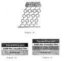
- Figure 1 represent graphical illustrations of the layer system of the present invention: two different layer arrangements are shown in Figures 1b and 1c.
- Figure 1a is a graphical illustration of cross-linked TPDMT on a substrate and, deposited thereon, a layer of metallic atoms.
- the profiles were measured by subsequent acquisition of the ISS spectra of Ni and Au during the erosion of the samples by the He + beam.
- the depth profiles of Ni were acquired 5 min (up triangles) and 24 hours (upside down triangles) after Ni deposition.
- the SAM region is marked gray.
- the irradiation dose was 45 mC/cm 2 .
- Figure 4 illustrates the difference of the NEXAFS spectra acquired at X-ray incidence angles of 90° and 20° as a function of ⁇ Ni for pristine (a) and cross-linked (b) TPDMT/Au.
- the irradiation dose was 45 mC/cm 2 .
- Layer systems comprising a substrate, a monolayer of molecules which is chemisorbed on the substrate and cross-linked in the lateral direction are known in the art.
- WO 01/23962 A2 describes such a system.
- the monolayer of molecules can be prepared both on a bulk support and on a thin film (bottom working layer) deposited on a bulk support, forming a sandwich structure as far as the monomolecular film is covered by a top working layer (see Figure 1).
- the thickness of the bottom working layer can range from several monolayers to several tens or even hundreds nm.
- metallic, semiconductor or oxide substrates can be used as to the substrate material. Preferred examples thereof comprise gold, silver, copper, aluminum, iron, cobalt, nickel, platinum, and alloys or mixtures thereof, as well as silicon, germanium, gallium arsenide, indium-tin oxide, all of which may possibly be doped to modify the semiconductor properties, as well as alloys thereof. Particularly for use as a gate dielectric, doped silicon is preferred as the substrate.
- the substrate is preferably ferromagnetic, substrates made of iron, cobalt, and/or nickel being particularly preferred.
- the laterally cross-linked monolayer of the layer system according to the invention is composed of chemisorbed molecules.
- the chemisorbed molecules have preferably a molecular weight of less than 1000, more preferably less than 500. They are preferably capable of forming self-assembled monolayers.
- the chemisorbed molecules preferably comprise an aromatic or heteroaromatic moiety, particularly preferred aromatic moieties being selected from the group consisting of phenyl, biphenyl, terphenyl, naphthalene, and anthracene, and particularly preferred heteroaromatic moieties are selected from the group consisting of bipyridine, terpyridine, thiophene, bithienyl, terthienyl, and pyrrole. Terphenyl is particularly preferred.
- the compounds forming the cross-linked monolayer comprise a group for chemisorption on the substrate (in the following referred to as the "anchor group”). Moreover, the compounds have preferably a functional group at the opposite end of the molecule, in a preferred embodiment at the opposite end of the aromatic/heteroaromatic backbone.
- the choice of the functional group depends on the material of the top layer to get a chemical linkage by building individual bonds between the functional groups and atoms or molecules of the top layer.
- Preferred functional groups are -SH, -OH, -COOH, - COOH 3 , -CH 2 OH, -NH 2 , and -NO 2 .
- the thiol group (-SH) is particularly preferred, especially if the top layer is composed of a metal.
- the anchor group that chemically anchors the monolayer constituents to the substrate is selected according to the substrate material (see below).
- carboxy, thiol, selenol, trichlorosilyl, trialkoxysilyl, phosphonate, hydroxamic acid, and phosphate groups can be used.
- the anchor groups is either directly bound to the aromatic and/or heteroaromatic spacer or there can be a linker, e.g. a chain of 1 to 6 methylene groups between the headgroup and spacer, e.g. to achieve a better molecular packing.
- anchor group is tailored to the particular substrate material, in a way known to one skilled in the art.
- trichlorosilanes or trialkoxysilanes such as trimethyloxysilane, triethoxysilane, etc. are particularly suitable as anchor groups for oxidized silicon surfaces.
- Alcohol groups can be used for anchoring for hydrogenated silicon surfaces.
- thiol or selenol groups can be used as anchor groups; for oxidized metal surfaces such as iron or chromium, suitable anchor groups are phosphonic acids, carboxylic acids, or hydroxamic acids.
- the layer system includes a monolayer composed of molecules satisfying the general formula An-Ar-Fn, wherein An is the anchor group as defined above, optionally comprising a spacer, Ar is the aromatic/heteroaromatic moiety as defined above, and Fn is the functional group as defined above, optionally comprising a spacer.
- Particularly preferred compounds of the above formula comprise [1,1'-biphenyl]-4,4'-dimethanethiol (BPDMT) and [1,1';4',1"-terphenyl]-4,4'-dimethanethiol (TPDMT).
- the present invention thus allows the fabrication of a monomolecular thick insulation film (on any substrate, including thin film) in a SAM fashion, with the subsequent fabrication of a top working (e.g. electrically conductive, ferromagnetic, or organic) layer.
- the fabrication procedure may combine specific functionalization of the film's constituents with their extensive cross-linking in the lateral direction. While the functionalization ensures 2D growth and chemical adherence of the working layer, the cross-linking closes the diffusion channels, ensuring the persistence of the working layer constituents on the insulator film surface and thus the insulation properties of the monomolecular film.
- the layer systems of the present invention can be prepared in the following series of process steps:
- a bulk substrate suitable for a particular application should be selected and cleaned.
- the bulk substrate should be freshly prepared, e.g. as a thick film.
- the surface of the bulk substrate can be, if necessary, chemically modified to provide a chemical link to the anchor groups of the SAM constituents.
- Another possibility is the deposition of a thin film, serving as the bottom working layer (see Figure 1).
- the pristine SAM is formed by e.g. immersion procedure or evaporation from the gas phase.
- the choice of the SAM constituents and, in particular, the anchor and functional groups depends on the substrate (or bottom working layer) and top working layer.
- step (d) the monolayer is cross-linked by its extensive irradiating.
- electron, X-ray, or UV irradiation may be employed.
- a large-area illuminating electron source can be used, such as e.g. a "flood gun” or a set-up as described in Fig. 2 of Hild et al., Langmuir, 14, 342-346 (1998) .
- the electron energies from 10 to several hundreds eV can be used.
- step (c) instead of applying a monolayer of aromatic and/or heteroaromatic compounds, compounds with partially or completely hydrogenated aromatic or heteroaromatic moieties, such as cyclohexyl, bicyclohexyl, tercyclohexyl, partially or completely hydrogenated naphthalene or anthracene, are applied, dehydrogenation to the corresponding aromatic or heteroaromatic compounds can occur in step (d), in addition to cross-linking in the lateral direction.
- partially or completely hydrogenated aromatic or heteroaromatic moieties such as cyclohexyl, bicyclohexyl, tercyclohexyl, partially or completely hydrogenated naphthalene or anthracene
- the cross-linking can be carried out with lateral structuring, e.g. by means of a finely focused ionising electron, ion, or photon beam radiation.
- a large-area illuminating electron source combined with a shadow mask can be used for lateral structuring, so that only the open areas are exposed to the electrons.
- Also suitable for lateral structuring are focused electron or X-ray beams, provided by suitable experimental setups and scanned over the sample surface.
- masks appropriate for the respective wavelength range or scanning by means of a suitable light guide are available.
- the top layer e.g. electrically conductive layer
- the compounds contain a nitro group as a functional group (Fn)
- these nitro groups can also be converted to amino groups in the impact zone of the cross-linking beam radiation in step (d).
- the top working layer can be an electrically conductive layer (e.g. gold, silver, copper, or aluminium), ferromagnetic layer (e.g. iron, cobalt, or nickel) or a semiconductor layer. Besides metals, organic semiconductors such as e.g. pentacene may also be used. Ferromagnetic layers are particularly preferred, for example layers made of nickel, iron, or cobalt, particularly if the substrate is also ferromagnetic.
- the fabrication of the top working layer can be performed by different means, e.g. by its deposition from the gas phase, from a metal or organic evaporated, or by electrochemical means.
- the monolayer is preferably a self-assembled monolayer, i.e. is a well-ordered and densely packed organic film, as, e.g., confirmed by NEXAFS spectroscopy.
- Its thickness is preferably in the range of 0.3 to 5 nm, more preferably in the range of 1.2 to 3 nm.
- the thickness is mainly determined by the length of the film constituents, corrected for their tilt in the film (the average tilt angle can be derived by IR or NEXAFS spectroscopy).
- the thickness can be directly estimated by ellipsometry or X-ray photoemission, using either the substrate or adsorbate signals or both of them. According to the present invention, X-ray photoemission is the preferred method for measuring the thickness.
- the layer system of the present invention has preferably a resistance of 10 M ⁇ cm 2 or more, more preferably in the range of 12 to 20 M ⁇ cm 2 .
- the resistance can be, e.g., determined by electrochemical measurements, i.e. impedance spectroscopy or using conducting probe atomic force microscopy (see e.g. Wold et al, J. Phys. Chem. B 106, 2813 (2002 )) or mercury drop method (see e.g. Holmlin et al., J. Am. Chem. Soc. 123, 5075 (2001 )).
- impedance spectroscopy is the preferred method for measuring the resistance.
- the layer system of the present invention has preferably a capacitance of 0.8 ⁇ F cm 2 or more, more preferably in the range of 1 to 1.5 ⁇ F cm 2 .
- the capacitance can be, e.g., determined using electrochemical measurements, i.e. impedance spectroscopy.
- the use of the monomolecular insulator film of the present invention in microelectronic devices can provide significant advantages.
- the application of such a film as a gate dielectric in organic thin film transistors can result in lowering of the operation voltage and a better performance of such a device (cf. Halik et al., Nature, 431, 963 (2004 )).
- the use of the monomolecular insulator film of the present invention as the insulator in a tunnel junction magnetic memory cell Kortright et al., J. Magn. Magn, Mat. 207, 7 (1999 ); Tsymball et al., J. Phys. Condens. Matter.
- the invention thus provides a trilayer system, comprising a ferromagnetic bottom film, a monolayer of molecules chemisorbed on it, and an ferromagnetic layer on the top of the monolayer, the monolayer of chemisorbed molecules being defined as detailed above.
- Gold substrates were prepared by thermal evaporation of 100 nm of gold onto Si(100) wafers (Silicon Sense) primed with a 5 nm titanium adhesion layer.
- the resulting metal films were polycrystalline, with a grain size of 20-50 nm. The grains predominantly exhibit an (111) orientation.
- SAMs were prepared by immersion of the Au substrates in the solution of [1,1' ;4' ,1" -terphenyl]-4,4"-dimethanethiol (TPDMT) (for details, see Shaporenko et al., J. Phys. Chem. B 108, 14462 (2004 ); Tai et al., J. Phys. Chem.
- Ni (Goodfellow, 99.999% purity) was evaporated from a commercial e-beam evaporator (Omicron) with a deposition rate of 0.2 nm per minute; the rate was calibrated by a commercial quartz crystal microbalance sensor (Inficon). The evaporation was performed at a base pressure better than 1.5x10 -9 Torr; the substrates were kept at room temperature.
- the pristine SAMs were characterized by XPS, NEXAFS spectroscopy, Infrared-Reflection Absorption Spectroscopy, ellipsometry, and contact angle measurements.
- the evaporation of Ni was monitored by XPS, NEXAFS spectroscopy, ISS, AFM, and electrochemical measurements. All experiments were performed at room temperature.
- the XPS, HRXPS, ISS, and NEXAFS spectroscopy measurements were carried out in-situ, under UHV conditions. AFM and electrochemical measurements were performed ex-situ.
- the XPS experiments were carried out using two different spectrometers. One of them was equipped with a Mg K ⁇ X-ray source and a LHS11 analyzer. The other used a synchrotron light (HE-SGM, BESSY II) as the primary source and was equipped with a VG CLAM 2 analyzer.
- the spectra acquisition was carried out at variable emission geometry with an energy resolution of approx. 0.9 eV and approx. 0.4 eV, respectively.
- the energy scale was referenced to the Au 4f 7/2 peak at 84.0 eV.
- the NEXAFS measurements were performed at the HE-SGM beamline of the synchrotron storage ring BESSY II in Berlin, Germany.
- the spectra acquisition was carried out at the carbon K-edge in the partial electron yield mode with a retarding voltage of -150 V.
- Linear polarized synchrotron light with a polarization factor of approx. 82% was used.
- the energy resolution was approx. 0.40 eV.
- the incidence angle of the light was varied to monitor the orientational order within the films. This approach is based on the linear dichroism in X-ray absorption, i.e.
- the raw NEXAFS spectra were normalized to the incident photon flux by division through a spectrum of a clean, freshly sputtered gold sample.
- the energy scale was referenced to the pronounced ⁇ 1 * resonance of highly oriented pyrolytic graphite (HOPG) at 285.38 eV.
- HOPG highly oriented pyrolytic graphite
- ISS measurements were performed with a focused ion gun (Leybold-Heraeus) and a LHS 11 analyzer.
- the primary ion beam He + , MESSER 99.999%) was accelerated to 1 keV and operated at a current of approx. 100 nA/cm 2 .
- the beam was focused to a spot with a diameter of ca. 500 ⁇ m by two focal lenses.
- the angle between the primary beam and sample surface was 35°.
- the beam was rastered over a 2 x 2 mm 2 area, which was gated with a 70% aperture.
- the depth profiles of Ni and Au were measured by subsequent acquisition of the ISS spectra (both the Ni and Au signals were recorded in a single scan) with an energy window from 750 to 1000 eV during the erosion of the samples by the ISS beam.
- AFM measurements were carried out with a Park Scientific Instruments "AutoProbe" model in ambient.
- a 5 ⁇ m scanner and a cantilever with silicon nitride (Si 3 N 4 ) tip were used.
- the applied force was set to 12 nN
- the gain was set to c.a. 1, with a scan rate of c.a. 2 Hz.
- an area of 2x2 ⁇ m 2 was scanned.
- the mean surface roughness RMS: root mean square
- Electrochemical measurements which included cyclic voltammetry and impedance spectroscopy, were carried out with an impedance measurement unit (IM6e, ZAHNER Elektrik) under an argon gas atmosphere at room temperature.
- An Ag/AgCl electrode and a Pt mesh electrode were used as the reference and counter electrodes, respectively.
- An aqueous solution of 0.1 M HClO 4 was used as an electrolyte. Prior to the electrochemical measurements, the electrolyte solution was deaerated by bubbling argon gas for 15 min. Cyclic voltammograms were measured with a constant scan rate of 0.1 V s -1 in the potential range between 0 and 0.6 V.
- Impedance spectra were taken between 100 kHz and 50 MHz under sinusoidal potentials with an amplitude of 10 mV.
- the whole system was represented by ideal elements of a simplified equivalent circuit model composed of serial resistance R s , interface capacitance C, and interface resistance R P .
- the impedance spectrum of the bare gold electrode was measured and the respective electrochemical parameters were calculated, assuming a double-layer formation at the gold electrode/electrolyte interface and the ohmic behaviour of the electrolyte solution and the contacts in the highfrequency regime.
- ISS is a technique that is capable to provide a direct information on the depth distribution of the metal adsorbate.
- an ion beam is directed onto a surface, and the energy distribution of the scattered ions is measured (a typical cross-section for the scattering is about 5-10 ⁇ 10 19 cm 2 /sr), which can be easily converted into mass spectra ( E. Taglauer, in Surface Analysis - The Principal Techniques, Ed. J. C. Vickerman, Wiley, Chichester, 1997 ).
- the erosion of the samples occurs, so that a depth profile of the mass of interest can be acquired by subsequent collection of the ISS spectra.
- Ni/TPMT/Au no Ni is observed at the SAM-ambient interface - all metal adsorbate atoms penetrated into the SAM and diffused to the SAM-Au interface.
- the Ni ISS profiles for Ni/TPDMT/Au (pristine), show a pronounced Ni signal on the SAM surface, but even a stronger signal at the SAM-Au interface, which can be easily traced by the appearing Au signal (the further growth of the Ni signal is related to the formation of a Ni-Au alloy)( Bigault et al., Phys. Rev.
- the formation of the Ni film on the top of the TPDMT film is accompanied by the penetration of Ni to the SAM-Au interface.
- the penetration process is favoured by an extended SAM reorientation, mediated by the formation of Ni-thiol complexes at the SAM-ambient interface (see Tai et al., Appl. Phys. Lett. 85, 6257 (2004 )). This results in the appearance of additional transient channels for the metal diffusion into the SAM and to the SAM-substrate interface.
- NEXAFS data show that the orientational order in this film persists upon Ni evaporation and film formation.
- NEXAFS spectra presented in Figure 4b.
- Such spectra are a direct fingerprint of the orientational order and molecular tilt in the film - an oriented film exhibits pronounced difference peaks at the positions of the characteristic absorption resonances.
- the positive sign of the ⁇ 1 * peak (at approx. 285 eV) in the spectra in Figure 4b is characteristic of an upright orientation of the SAM constituents, which is obviously preserved, even though a Ni layer is formed on top of the SAM.
- This Ni film formed on the surface of CL-TPDMT/Au is stable, as shows the comparison between the ISS profiles of Ni taken in 3 min and 24 hours after the evaporation ( Figure 2c).
- the presence of the thiol tailgroups improves the adherence of the Ni film to the SAM support - due to the chemical anchoring by formation of Ni thiolate links at the SAM-ambient interface.
Landscapes
- Engineering & Computer Science (AREA)
- Chemical & Material Sciences (AREA)
- Nanotechnology (AREA)
- Physics & Mathematics (AREA)
- Crystallography & Structural Chemistry (AREA)
- Condensed Matter Physics & Semiconductors (AREA)
- General Physics & Mathematics (AREA)
- Composite Materials (AREA)
- Manufacturing & Machinery (AREA)
- Materials Engineering (AREA)
- Mathematical Physics (AREA)
- Theoretical Computer Science (AREA)
- Thin Film Transistor (AREA)
- Polymers With Sulfur, Phosphorus Or Metals In The Main Chain (AREA)
- Electrodes Of Semiconductors (AREA)
- Formation Of Insulating Films (AREA)
Abstract
Description
- The present invention relates to a layer system with a monolayer thick organic thin film having electrical insulation properties, and a microelectronic or spintronic device comprising the same, such as e.g. a field effect transistor or a magnetic tunnel junction.
- Self-assembled monolayers (SAMs) are well-ordered and densely packed organic films, composed of chemisorbed rod-like molecules (see A. Ulman, An Introduction to Ultrathin Organic Films: Langmuir-Blodgett to Self-Assembly; Academic Press: New York, 1991; Chem. Rev. 96, 1533 (1996)). Their use has been proposed for new materials in electronics and spintronics. For example, SAMs have the potential to be used as ultrathin insulator layers in standard and newly designed electronic elements, providing an alternative to commonly used oxide dielectrics such as e.g. SiO2 or Al2O3. A barrier for the above-mentioned applications of SAMs is the difficulty to fabricate a stable metal layer on their surface, i.e. at the SAM-ambient interface. Such a layer could serve as the top electrode in a molecular device, as source and drains electrodes in thin film transistors, or as the top ferromagnetic layer in a magnetic tunnel junction.
- Despite the cartoons representing well-defined metal-SAM-substrate structures found in the literature (see e.g. Schön et al., Nature 413, 713 (2001)), a stable metal layer on top of a SAM has not been demonstrated yet. Studies of metal adsorption onto the SAM surface show that metal atoms usually penetrate into the SAM layer and diffuse to the SAM-substrate interface (see Czanderna and D. R. Jung, Crit. Rev. Sol. State. Mat. Sci. 19, 1 (1994); Epple et al., Langmuir 18, 773 (2002); Walker et al., Appl. Phys. Lett. 84, 4008 (2004)). Diffusion occurs over static and dynamic transient channels, which are structural defects in the SAM (e.g. domain boundaries, etc.) and irregularities related to the moving of the SAM constituents (see Hooper et al., J. Am. Chem. Soc. 121, 8052 (1999); Fisher et al., J. Am. Chem. Soc. 124, 5528 (2002)). In this regard, the SAM homogeneity is important, since it affects the density of the transient channels. While it has been reported that diffusion into the organic film can be reduced for selective systems e.g. by cooling or introduction of reactive functional groups (Czanderna et al., Crit. Rev. Sol. State. Mat. Sci. 19, 1 (1994); Hooper et al., J. Am. Chem. Soc. 121, 8052 (1999); Fisher et al., J. Am. Chem. Soc. 124, 5528 (2002);Weckenmann, et al., Chem. Mater. 16, 621 (2004); de Boer et al., Langmuir 20, 1539 (2004)), none of the described systems is fully satisfactory in terms of stability and insulation properties. Moreover, none of the described systems provides an electrically conductive layer of a metal of relatively low reactivity, such as nickel, cobalt, or iron, on top of a self-assembled monolayer.
- It is the object underlying the present invention to provide such systems and microelectronic devices containing the same.
- To solve this objective, the present invention provides a layer system, comprising a substrate, being either a bulk substrate or a thin film deposited on it, a monolayer of organic molecules, which is chemisorbed on the substrate and cross-linked in the lateral direction, and a deposited layer on top of the monolayer. The present invention also provides a microelectronic device comprising the layer system of the present invention, such as e.g. a field effect transistor or a tunnel junction magnetic memory cell.
- Figure 1 represent graphical illustrations of the layer system of the present invention: two different layer arrangements are shown in Figures 1b and 1c. Figure 1a is a graphical illustration of cross-linked TPDMT on a substrate and, deposited thereon, a layer of metallic atoms.
- Figure 2 shows the ISS depth profiles for Ni and Au (open circles) after Ni deposition on TPMA/Au (Figure 2a), TPDMT/Au (Figure 2b) and cross-linked TPDMT/Au (Figure 2c), respectively (θNi=10.0). The profiles were measured by subsequent acquisition of the ISS spectra of Ni and Au during the erosion of the samples by the He+ beam. The depth profiles of Ni were acquired 5 min (up triangles) and 24 hours (upside down triangles) after Ni deposition. The SAM region is marked gray.
- Figure 3 shows relative intensities of the C 1s (upward triangles, solid line) and Ni 2p (upside down triangles, dashed line) XPS signals as a function of the photoelectron takeoff angle for Ni deposited on pristine (a) and cross-linked (b) TPDMT/Au (θNi=10.0). The irradiation dose was 45 mC/cm2.
- Figure 4 illustrates the difference of the NEXAFS spectra acquired at X-ray incidence angles of 90° and 20° as a function of ΘNi for pristine (a) and cross-linked (b) TPDMT/Au. The irradiation dose was 45 mC/cm2.
- Layer systems comprising a substrate, a monolayer of molecules which is chemisorbed on the substrate and cross-linked in the lateral direction are known in the art. For example,
WO 01/23962 A2 - The monolayer of molecules can be prepared both on a bulk support and on a thin film (bottom working layer) deposited on a bulk support, forming a sandwich structure as far as the monomolecular film is covered by a top working layer (see Figure 1). The thickness of the bottom working layer can range from several monolayers to several tens or even hundreds nm. As to the substrate material, metallic, semiconductor or oxide substrates can be used. Preferred examples thereof comprise gold, silver, copper, aluminum, iron, cobalt, nickel, platinum, and alloys or mixtures thereof, as well as silicon, germanium, gallium arsenide, indium-tin oxide, all of which may possibly be doped to modify the semiconductor properties, as well as alloys thereof. Particularly for use as a gate dielectric, doped silicon is preferred as the substrate. For magnetic tunnel junctions, the substrate is preferably ferromagnetic, substrates made of iron, cobalt, and/or nickel being particularly preferred.
- The laterally cross-linked monolayer of the layer system according to the invention is composed of chemisorbed molecules. The chemisorbed molecules have preferably a molecular weight of less than 1000, more preferably less than 500. They are preferably capable of forming self-assembled monolayers. The chemisorbed molecules preferably comprise an aromatic or heteroaromatic moiety, particularly preferred aromatic moieties being selected from the group consisting of phenyl, biphenyl, terphenyl, naphthalene, and anthracene, and particularly preferred heteroaromatic moieties are selected from the group consisting of bipyridine, terpyridine, thiophene, bithienyl, terthienyl, and pyrrole. Terphenyl is particularly preferred.
- The compounds forming the cross-linked monolayer comprise a group for chemisorption on the substrate (in the following referred to as the "anchor group"). Moreover, the compounds have preferably a functional group at the opposite end of the molecule, in a preferred embodiment at the opposite end of the aromatic/heteroaromatic backbone. The choice of the functional group depends on the material of the top layer to get a chemical linkage by building individual bonds between the functional groups and atoms or molecules of the top layer. Preferred functional groups are -SH, -OH, -COOH, - COOH3, -CH2OH, -NH2, and -NO2. The thiol group (-SH) is particularly preferred, especially if the top layer is composed of a metal.
- The anchor group that chemically anchors the monolayer constituents to the substrate is selected according to the substrate material (see below). In particular, carboxy, thiol, selenol, trichlorosilyl, trialkoxysilyl, phosphonate, hydroxamic acid, and phosphate groups can be used. In a preferred embodiment, the anchor groups is either directly bound to the aromatic and/or heteroaromatic spacer or there can be a linker, e.g. a chain of 1 to 6 methylene groups between the headgroup and spacer, e.g. to achieve a better molecular packing.
- The nature of the anchor group is tailored to the particular substrate material, in a way known to one skilled in the art. For example, trichlorosilanes or trialkoxysilanes such as trimethyloxysilane, triethoxysilane, etc. are particularly suitable as anchor groups for oxidized silicon surfaces. Alcohol groups can be used for anchoring for hydrogenated silicon surfaces. For noble and 3d metal substrates, thiol or selenol groups can be used as anchor groups; for oxidized metal surfaces such as iron or chromium, suitable anchor groups are phosphonic acids, carboxylic acids, or hydroxamic acids.
- In a particularly preferred embodiment of the present invention, the layer system includes a monolayer composed of molecules satisfying the general formula An-Ar-Fn, wherein An is the anchor group as defined above, optionally comprising a spacer, Ar is the aromatic/heteroaromatic moiety as defined above, and Fn is the functional group as defined above, optionally comprising a spacer. Particularly preferred compounds of the above formula comprise [1,1'-biphenyl]-4,4'-dimethanethiol (BPDMT) and [1,1';4',1"-terphenyl]-4,4'-dimethanethiol (TPDMT).
- The present invention thus allows the fabrication of a monomolecular thick insulation film (on any substrate, including thin film) in a SAM fashion, with the subsequent fabrication of a top working (e.g. electrically conductive, ferromagnetic, or organic) layer. The fabrication procedure may combine specific functionalization of the film's constituents with their extensive cross-linking in the lateral direction. While the functionalization ensures 2D growth and chemical adherence of the working layer, the cross-linking closes the diffusion channels, ensuring the persistence of the working layer constituents on the insulator film surface and thus the insulation properties of the monomolecular film.
- The layer systems of the present invention can be prepared in the following series of process steps:
- (a) selection and preparation of a bulk substrate,
- (b) modification of the bulk substrate surface, if necessary,
- (c) fabrication of the pristine monolayer
- (d) treatment of the substrate obtained in step (c) with high-energy beam radiation so that the monolayer is covalently cross-linked in the lateral direction,
- (e) adsorbing the metal atoms or organic molecules to provide the (e.g. electrically conductive) layer on top of the monolayer.
- In step (a), a bulk substrate suitable for a particular application should be selected and cleaned. In some cases, the bulk substrate should be freshly prepared, e.g. as a thick film.
- In step (b),the surface of the bulk substrate can be, if necessary, chemically modified to provide a chemical link to the anchor groups of the SAM constituents. Another possibility is the deposition of a thin film, serving as the bottom working layer (see Figure 1).
- In step (c), the pristine SAM is formed by e.g. immersion procedure or evaporation from the gas phase. The choice of the SAM constituents and, in particular, the anchor and functional groups depends on the substrate (or bottom working layer) and top working layer.
- In step (d), the monolayer is cross-linked by its extensive irradiating. For this purpose, electron, X-ray, or UV irradiation may be employed.
- For electron irradiation, a large-area illuminating electron source can be used, such as e.g. a "flood gun" or a set-up as described in Fig. 2 of Hild et al., Langmuir, 14, 342-346 (1998). The electron energies from 10 to several hundreds eV can be used.
- For large-area cross-linking by means of X-ray or UV irradiation, light sources available in the prior art can be used.
- If in step (c), instead of applying a monolayer of aromatic and/or heteroaromatic compounds, compounds with partially or completely hydrogenated aromatic or heteroaromatic moieties, such as cyclohexyl, bicyclohexyl, tercyclohexyl, partially or completely hydrogenated naphthalene or anthracene, are applied, dehydrogenation to the corresponding aromatic or heteroaromatic compounds can occur in step (d), in addition to cross-linking in the lateral direction.
- In one embodiment of the invention, the cross-linking can be carried out with lateral structuring, e.g. by means of a finely focused ionising electron, ion, or photon beam radiation.
- A large-area illuminating electron source combined with a shadow mask can be used for lateral structuring, so that only the open areas are exposed to the electrons. Also suitable for lateral structuring are focused electron or X-ray beams, provided by suitable experimental setups and scanned over the sample surface.
- For lateral structuring by means of electromagnetic radiation, masks appropriate for the respective wavelength range or scanning by means of a suitable light guide (optical fiber) are available.
- If lateral structuring is carried out, it is possible to provide a structured surface with areas having a high affinity to the metal atoms or organic molecules forming the (e.g. electrically conductive) top layer and areas having a low affinity to the metal atoms or organic molecules forming the (e.g. electrically conductive) top layer. Hence, the top layer (e.g. electrically conductive layer) can be provided in a pattern on the monolayer. For example, if the compounds contain a nitro group as a functional group (Fn), then these nitro groups can also be converted to amino groups in the impact zone of the cross-linking beam radiation in step (d).
- The top working layer can be an electrically conductive layer (e.g. gold, silver, copper, or aluminium), ferromagnetic layer (e.g. iron, cobalt, or nickel) or a semiconductor layer. Besides metals, organic semiconductors such as e.g. pentacene may also be used. Ferromagnetic layers are particularly preferred, for example layers made of nickel, iron, or cobalt, particularly if the substrate is also ferromagnetic.
- The fabrication of the top working layer can be performed by different means, e.g. by its deposition from the gas phase, from a metal or organic evaporated, or by electrochemical means.
- Even after adsorption, the monolayer is preferably a self-assembled monolayer, i.e. is a well-ordered and densely packed organic film, as, e.g., confirmed by NEXAFS spectroscopy.
- Its thickness is preferably in the range of 0.3 to 5 nm, more preferably in the range of 1.2 to 3 nm. The thickness is mainly determined by the length of the film constituents, corrected for their tilt in the film (the average tilt angle can be derived by IR or NEXAFS spectroscopy). The thickness can be directly estimated by ellipsometry or X-ray photoemission, using either the substrate or adsorbate signals or both of them. According to the present invention, X-ray photoemission is the preferred method for measuring the thickness.
- The layer system of the present invention has preferably a resistance of 10 MΩ cm2 or more, more preferably in the range of 12 to 20 MΩ cm2. The resistance can be, e.g., determined by electrochemical measurements, i.e. impedance spectroscopy or using conducting probe atomic force microscopy (see e.g. Wold et al, J. Phys. Chem. B 106, 2813 (2002)) or mercury drop method (see e.g. Holmlin et al., J. Am. Chem. Soc. 123, 5075 (2001)). According to the present invention, impedance spectroscopy is the preferred method for measuring the resistance.
- The layer system of the present invention has preferably a capacitance of 0.8 µF cm2 or more, more preferably in the range of 1 to 1.5 µF cm2. The capacitance can be, e.g., determined using electrochemical measurements, i.e. impedance spectroscopy.
- The use of the monomolecular insulator film of the present invention in microelectronic devices can provide significant advantages. For example, the application of such a film as a gate dielectric in organic thin film transistors can result in lowering of the operation voltage and a better performance of such a device (cf. Halik et al., Nature, 431, 963 (2004)). Also, the use of the monomolecular insulator film of the present invention as the insulator in a tunnel junction magnetic memory cell (Kortright et al., J. Magn. Magn, Mat. 207, 7 (1999); Tsymball et al., J. Phys. Condens. Matter. 15, R109 (2003)) can result in a better coupling of the ferromagnetic layers and help to avoid the problem of the ferromagnet-insulator interface degradation, which occurs due to the migration of oxygen from a conventional oxide insulator. In such a memory cell, the invention thus provides a trilayer system, comprising a ferromagnetic bottom film, a monolayer of molecules chemisorbed on it, and an ferromagnetic layer on the top of the monolayer, the monolayer of chemisorbed molecules being defined as detailed above.
- Gold substrates were prepared by thermal evaporation of 100 nm of gold onto Si(100) wafers (Silicon Sense) primed with a 5 nm titanium adhesion layer. The resulting metal films were polycrystalline, with a grain size of 20-50 nm. The grains predominantly exhibit an (111) orientation. Subsequently, SAMs were prepared by immersion of the Au substrates in the solution of [1,1' ;4' ,1" -terphenyl]-4,4"-dimethanethiol (TPDMT) (for details, see Shaporenko et al., J. Phys. Chem. B 108, 14462 (2004); Tai et al., J. Phys. Chem. B 108, 16806 (2004); Tai et al., Appl. Phys. Lett. 85, 6257 (2004)). After immersion, the samples were carefully rinsed with pure solvent and blown dry with argon. No evidence for impurities or oxidative degradation products was found. The fabricated TPMT and TPDMT films were then irradiated by electrons with a kinetic energy of 10 eV. The dose was calculated by multiplication of the exposure time by the current density (approx. 2.5 µA/cm2), which was calibrated by a Faraday cup. Ni (Goodfellow, 99.999% purity) was evaporated from a commercial e-beam evaporator (Omicron) with a deposition rate of 0.2 nm per minute; the rate was calibrated by a commercial quartz crystal microbalance sensor (Inficon). The evaporation was performed at a base pressure better than 1.5x10⁻⁹ Torr; the substrates were kept at room temperature.
- The pristine SAMs were characterized by XPS, NEXAFS spectroscopy, Infrared-Reflection Absorption Spectroscopy, ellipsometry, and contact angle measurements. The evaporation of Ni was monitored by XPS, NEXAFS spectroscopy, ISS, AFM, and electrochemical measurements. All experiments were performed at room temperature. The XPS, HRXPS, ISS, and NEXAFS spectroscopy measurements were carried out in-situ, under UHV conditions. AFM and electrochemical measurements were performed ex-situ.
- The XPS experiments were carried out using two different spectrometers. One of them was equipped with a Mg Kα X-ray source and a LHS11 analyzer. The other used a synchrotron light (HE-SGM, BESSY II) as the primary source and was equipped with a VG CLAM 2 analyzer. The spectra acquisition was carried out at variable emission geometry with an energy resolution of approx. 0.9 eV and approx. 0.4 eV, respectively. The energy scale was referenced to the Au 4f7/2 peak at 84.0 eV.
- The NEXAFS measurements were performed at the HE-SGM beamline of the synchrotron storage ring BESSY II in Berlin, Germany. The spectra acquisition was carried out at the carbon K-edge in the partial electron yield mode with a retarding voltage of -150 V. Linear polarized synchrotron light with a polarization factor of approx. 82% was used. The energy resolution was approx. 0.40 eV. The incidence angle of the light was varied to monitor the orientational order within the films. This approach is based on the linear dichroism in X-ray absorption, i.e. the strong dependence of the cross-section of the resonant photoexcitation process on the orientation of the electric field vector of the linearly polarized light with respect to the molecular orbital of interest. The raw NEXAFS spectra were normalized to the incident photon flux by division through a spectrum of a clean, freshly sputtered gold sample. The energy scale was referenced to the pronounced π1* resonance of highly oriented pyrolytic graphite (HOPG) at 285.38 eV.
- ISS measurements were performed with a focused ion gun (Leybold-Heraeus) and a LHS 11 analyzer. The primary ion beam (He+, MESSER 99.999%) was accelerated to 1 keV and operated at a current of approx. 100 nA/cm2. The beam was focused to a spot with a diameter of ca. 500 µm by two focal lenses. The angle between the primary beam and sample surface was 35°. During data acquisition, the beam was rastered over a 2 x 2 mm2 area, which was gated with a 70% aperture. The depth profiles of Ni and Au were measured by subsequent acquisition of the ISS spectra (both the Ni and Au signals were recorded in a single scan) with an energy window from 750 to 1000 eV during the erosion of the samples by the ISS beam.
- AFM measurements were carried out with a Park Scientific Instruments "AutoProbe" model in ambient. A 5 µm scanner and a cantilever with silicon nitride (Si3N4) tip were used. In most experiments, the applied force was set to 12 nN, the gain was set to c.a. 1, with a scan rate of c.a. 2 Hz. Usually, an area of 2x2 µm2 was scanned. From the measurements, the mean surface roughness (RMS: root mean square) was directly evaluated.
- Electrochemical measurements, which included cyclic voltammetry and impedance spectroscopy, were carried out with an impedance measurement unit (IM6e, ZAHNER Elektrik) under an argon gas atmosphere at room temperature. An Ag/AgCl electrode and a Pt mesh electrode were used as the reference and counter electrodes, respectively. An aqueous solution of 0.1 M HClO4 was used as an electrolyte. Prior to the electrochemical measurements, the electrolyte solution was deaerated by bubbling argon gas for 15 min. Cyclic voltammograms were measured with a constant scan rate of 0.1 V s-1 in the potential range between 0 and 0.6 V. Impedance spectra were taken between 100 kHz and 50 MHz under sinusoidal potentials with an amplitude of 10 mV. To estimate the electrochemical parameters from the data, the whole system was represented by ideal elements of a simplified equivalent circuit model composed of serial resistance R s , interface capacitance C, and interface resistance R P . As the reference, the impedance spectrum of the bare gold electrode was measured and the respective electrochemical parameters were calculated, assuming a double-layer formation at the gold electrode/electrolyte interface and the ohmic behaviour of the electrolyte solution and the contacts in the highfrequency regime.
- ISS is a technique that is capable to provide a direct information on the depth distribution of the metal adsorbate. In ISS experiment, an ion beam is directed onto a surface, and the energy distribution of the scattered ions is measured (a typical cross-section for the scattering is about 5-10×10 19 cm2/sr), which can be easily converted into mass spectra (E. Taglauer, in Surface Analysis - The Principal Techniques, Ed. J. C. Vickerman, Wiley, Chichester, 1997). In parallel, the erosion of the samples occurs, so that a depth profile of the mass of interest can be acquired by subsequent collection of the ISS spectra. Under the conditions of the experiments (3He+, 1 keV, 100 nA/cm2, a scattering angle of 55°) , the erosion rate was about 0.05-0.1 Å/min, and no ion-induced intermixing occurred (Chenakin et al., Surf. Sci. 397, 84 (1998) ; 421, 337 (1999)).
- The ISS depth profiles of Ni and Au for Ni/TPMT/Au and Ni/TPDMT/Au (θNi=10.0) are presented in Figures 2a and 2b,respectively. For Ni/TPMT/Au, no Ni is observed at the SAM-ambient interface - all metal adsorbate atoms penetrated into the SAM and diffused to the SAM-Au interface. The Ni ISS profiles for Ni/TPDMT/Au (pristine), show a pronounced Ni signal on the SAM surface, but even a stronger signal at the SAM-Au interface, which can be easily traced by the appearing Au signal (the further growth of the Ni signal is related to the formation of a Ni-Au alloy)(Bigault et al., Phys. Rev. B 64, 125414 (2001)). Thus, the formation of the Ni film on the top of the TPDMT film is accompanied by the penetration of Ni to the SAM-Au interface. The penetration process is favoured by an extended SAM reorientation, mediated by the formation of Ni-thiol complexes at the SAM-ambient interface (see Tai et al., Appl. Phys. Lett. 85, 6257 (2004)). This results in the appearance of additional transient channels for the metal diffusion into the SAM and to the SAM-substrate interface.
- The same analysis was carried out after cross-linking (CL) of the TPDMT films by electron irradiation. The respective Ni ISS depth profile in Figure 2c taken immediately after Ni evaporation exhibits a strong Ni signal on the top of the SAM and no signal within the SAM or at the SAM-Au interface. Thus, the diffusion of Ni into the film appears to be significantly reduced, and the Ni film is exclusively formed on the SAM surface.
- This result is supported by the XPS data presented in Figure 3b. For CL-TPDMT/Au, XPS signal of Ni remains almost constant with increasing takeoff angle of the photoelectrons, whereas the carbon signal decreases due to the increasing attenuation by the nickel overlayer. This behaviour is just opposite to the respective angle dependences for the pristine TPDMT/Au (Figure 3a), where a dramatic decrease in the Ni signal and a persistence of the carbon signal with increasing takeoff angle of the photoelectrons are observed.
- Further evidence that no penetration of Ni into CL-TPDMT/Au occurs is provided by NEXAFS data, which show that the orientational order in this film persists upon Ni evaporation and film formation. This is evidenced by the invariability of the respective difference NEXAFS spectra, presented in Figure 4b. Such spectra are a direct fingerprint of the orientational order and molecular tilt in the film - an oriented film exhibits pronounced difference peaks at the positions of the characteristic absorption resonances. The positive sign of the π1* peak (at approx. 285 eV) in the spectra in Figure 4b is characteristic of an upright orientation of the SAM constituents, which is obviously preserved, even though a Ni layer is formed on top of the SAM. In the case of the Ni penetration, the orientational order is destroyed, which was observed for all systems of this study except for CL-TPDMT. An example is given in Figure 4a, where the difference NEXAFS spectra for the pristine TPDMT/Au are presented. The amplitude of the difference peaks decreases in the course of the Ni evaporation, until it becomes negligibly small at θNi = 5-10, which corresponds to a fully disordered film. Note that a similar disordering is typical for metal adsorption onto the SAM substrates described in previous work (Czanderna et al., Crit. Rev. Sol. State Mat. Sci. 1994, 19, 1; Epple et al., Langmuir 2002, 18, 773 ; Walker et al. Appl. Phys. Lett. 2004, 84, 4008).
- This Ni film formed on the surface of CL-TPDMT/Au is stable, as shows the comparison between the ISS profiles of Ni taken in 3 min and 24 hours after the evaporation (Figure 2c).
AFM data suggest a low roughness of this film, which is presumably related to the occurrence of the nucleation centres for the film growth, provided by the thiol headgroups. Without these centres, a 3D growth mode for the Ni overlayer will occur, - the roughness (RMS: root mean square) of this layer increases by a factor of 5 as compared to Ni/CL-TPDMT/Au, where it was less than 0.5 nm (θNi=5-6).
In addition, the presence of the thiol tailgroups improves the adherence of the Ni film to the SAM support - due to the chemical anchoring by formation of Ni thiolate links at the SAM-ambient interface. - The persistence of the orientational order and full suppression of the Ni diffusion into the SAM are good prerequisites for device applications of CL-TPDMT/Au. Electrochemical measurements showed that the insulator properties of this film are not affected by Ni evaporation - the resistance and capacitance of the cross-linked SAM in the Ni-TPDMT-Au sandwich are 13.6 MΩ cm2 and 1.1 µF cm-2, respectively, which are very close to the values, which were observed for this film before Ni evaporation (14.4 MΩ cm2 and 1.36 µF cm-2, respectively). Interestingly, the cross-linking even improves the insulator parameters of the TPDMT layer - the resistance of the pristine TPDMT film was estimated as 5.7 MΩcm2.
Claims (14)
- A layer system, comprising a substrate, being either a bulk substrate or a thin film deposited on it, a monolayer of organic molecules chemisorbed on the substrate which is cross-linked in the lateral direction, and a deposited layer on top of the monolayer.
- The layer system according to claim 1, wherein the substrate is made of one or more of the metals gold, silver, copper, aluminium, iron, cobalt, nickel, or a semiconductor, the substrate being either a bulk substrate or a thin film deposited on it.
- The layer system according to any one of the preceding claims, wherein the top layer is an electrically conductive layer made of one or more of the metals gold, silver, copper, aluminium, or palladium.
- The layer system according to any one of the preceding claims, wherein the top layer is a ferromagnetic layer made of one or more 3d or 4d metals.
- The layer system according to claim 4, wherein the substrate is ferromagnetic, the substrate being either a bulk substrate or a thin film deposited on it.
- The layer system according to any one of claims 1 or 2, wherein the top layer is a semiconductor or an organic layer.
- The layer system according to any one of the preceding claims, wherein the chemisorbed molecules comprise an aromatic or heteroaromatic moiety.
- The layer system according to claim 7, wherein the aromatic or heteroaromatic moiety is selected from the group consisting of phenyl, biphenyl, terphenyl, naphthalene, anthracene, pyridin, bipyridin, terpyridin, thiophen, bithienyl, terthienyl, and pyrrol.
- The layer system according to any one of the preceding claims, wherein the chemisorbed molecules are cross-linkable by subjecting the same to electron irradiation, X-ray irradiation, or UV irradiation.
- The layer system according to any one of the preceding claims, wherein the chemisorbed molecules comprise a functional group selected from -SH, -OH, -COOH, -COOCH3, - CH2OH, or -NH2 on which the top layer is deposited.
- The layer system according to any one of the preceding claims, wherein the chemisorbed molecules form a self-assembled monolayer.
- The layer system according to any one of the preceding claims, which is a gate dielectric in a transistor assembly.
- The layer system film according to any one of claims 1 to 11, which is a magnetic tunnel junction.
- A microelectronic device comprising the layer system of one or more of the preceding claims.
Priority Applications (4)
| Application Number | Priority Date | Filing Date | Title |
|---|---|---|---|
| DE602005014847T DE602005014847D1 (en) | 2005-04-13 | 2005-04-13 | Organic thin-layered insulator |
| EP05008047A EP1712298B1 (en) | 2005-04-13 | 2005-04-13 | Organic thin film insulator |
| AT05008047T ATE433349T1 (en) | 2005-04-13 | 2005-04-13 | ORGANIC THIN FILM INSULATOR |
| PCT/EP2006/003385 WO2006108642A1 (en) | 2005-04-13 | 2006-04-12 | Organic thin film insulator |
Applications Claiming Priority (1)
| Application Number | Priority Date | Filing Date | Title |
|---|---|---|---|
| EP05008047A EP1712298B1 (en) | 2005-04-13 | 2005-04-13 | Organic thin film insulator |
Publications (2)
| Publication Number | Publication Date |
|---|---|
| EP1712298A1 true EP1712298A1 (en) | 2006-10-18 |
| EP1712298B1 EP1712298B1 (en) | 2009-06-10 |
Family
ID=34935092
Family Applications (1)
| Application Number | Title | Priority Date | Filing Date |
|---|---|---|---|
| EP05008047A Expired - Lifetime EP1712298B1 (en) | 2005-04-13 | 2005-04-13 | Organic thin film insulator |
Country Status (4)
| Country | Link |
|---|---|
| EP (1) | EP1712298B1 (en) |
| AT (1) | ATE433349T1 (en) |
| DE (1) | DE602005014847D1 (en) |
| WO (1) | WO2006108642A1 (en) |
Cited By (1)
| Publication number | Priority date | Publication date | Assignee | Title |
|---|---|---|---|---|
| WO2013008008A3 (en) * | 2011-07-14 | 2013-06-20 | Surface Innovations Limited | A method of producing a functionalized surface and surfaces made thereby |
Families Citing this family (4)
| Publication number | Priority date | Publication date | Assignee | Title |
|---|---|---|---|---|
| GB2527561B (en) | 2014-06-26 | 2021-06-16 | Cnm Tech Gmbh | Multilayer structure |
| US10586651B2 (en) | 2014-06-26 | 2020-03-10 | Cnm Technologies Gmbh | Method of manufacture of a multilayer structure |
| MX2017009473A (en) * | 2015-01-20 | 2017-11-02 | Basf Coatings Gmbh | Process for producing flexible organic-inorganic laminates. |
| US20170154790A1 (en) * | 2015-11-30 | 2017-06-01 | Intel Corporation | Sam assisted selective e-less plating on packaging materials |
Citations (4)
| Publication number | Priority date | Publication date | Assignee | Title |
|---|---|---|---|---|
| US5728431A (en) * | 1996-09-20 | 1998-03-17 | Texas A&M University System | Process for forming self-assembled polymer layers on a metal surface |
| WO2003008646A2 (en) * | 2001-07-17 | 2003-01-30 | Surmodics, Inc. | Method for making a self-assembling monolayer and composition |
| US6562398B1 (en) * | 1998-05-27 | 2003-05-13 | Commonwealth Scientific And Industrial Research Organization | Molecular coatings |
| US20040202875A1 (en) * | 1998-03-27 | 2004-10-14 | Yissum Res & Dev Co Of Hebrew Univ Of Jerusalem | Molecular epitaxy method and compositions |
-
2005
- 2005-04-13 DE DE602005014847T patent/DE602005014847D1/en not_active Expired - Fee Related
- 2005-04-13 AT AT05008047T patent/ATE433349T1/en not_active IP Right Cessation
- 2005-04-13 EP EP05008047A patent/EP1712298B1/en not_active Expired - Lifetime
-
2006
- 2006-04-12 WO PCT/EP2006/003385 patent/WO2006108642A1/en not_active Ceased
Patent Citations (4)
| Publication number | Priority date | Publication date | Assignee | Title |
|---|---|---|---|---|
| US5728431A (en) * | 1996-09-20 | 1998-03-17 | Texas A&M University System | Process for forming self-assembled polymer layers on a metal surface |
| US20040202875A1 (en) * | 1998-03-27 | 2004-10-14 | Yissum Res & Dev Co Of Hebrew Univ Of Jerusalem | Molecular epitaxy method and compositions |
| US6562398B1 (en) * | 1998-05-27 | 2003-05-13 | Commonwealth Scientific And Industrial Research Organization | Molecular coatings |
| WO2003008646A2 (en) * | 2001-07-17 | 2003-01-30 | Surmodics, Inc. | Method for making a self-assembling monolayer and composition |
Cited By (1)
| Publication number | Priority date | Publication date | Assignee | Title |
|---|---|---|---|---|
| WO2013008008A3 (en) * | 2011-07-14 | 2013-06-20 | Surface Innovations Limited | A method of producing a functionalized surface and surfaces made thereby |
Also Published As
| Publication number | Publication date |
|---|---|
| ATE433349T1 (en) | 2009-06-15 |
| DE602005014847D1 (en) | 2009-07-23 |
| EP1712298B1 (en) | 2009-06-10 |
| WO2006108642A1 (en) | 2006-10-19 |
Similar Documents
| Publication | Publication Date | Title |
|---|---|---|
| Polymeropoulos et al. | Electrical conduction through adsorbed monolayers | |
| Weiss et al. | Influence of defects on the electrical characteristics of mercury-drop junctions: self-assembled monolayers of n-alkanethiolates on rough and smooth silver | |
| Tarlov | Silver metalization of octadecanethiol monolayers self-assembled on gold | |
| Finklea | Electrochemistry of organized monolayers of thiols and related molecules | |
| Shirai et al. | Characterization of self-assembled monolayers of fullerene derivatives on gold surfaces: Implications for device evaluations | |
| Vericat et al. | Thiol-capped gold: from planar to irregular surfaces | |
| Xu et al. | The chemistry of self-assembled long-chain alkanethiol monolayers on gold | |
| Singh et al. | Adsorption of 3-mercaptopropyltrimethoxysilane on silicon oxide surfaces and adsorbate interaction with thermally deposited gold | |
| Tai et al. | Fabrication of Stable Metal Films on the Surface of Self‐Assembled Monolayers | |
| Itoh et al. | Surface potential of phthalocyanine Langmuir-Blodgett films on metal electrodes | |
| Gao et al. | Fabrication of asymmetric molecular junctions by the oriented assembly of dithiocarbamate rectifiers | |
| Pathak et al. | Disorder-derived, strong tunneling attenuation in bis-phosphonate monolayers | |
| Cerruti et al. | Influence of indium–tin oxide surface structure on the ordering and coverage of carboxylic acid and thiol monolayers | |
| EP1712298B1 (en) | Organic thin film insulator | |
| Aliganga et al. | Binary mixtures of self-assembled monolayers of 1, 8-octanedithiol and 1-octanethiol for a controlled growth of gold nanoparticles | |
| Scharf et al. | Electrochemical and surface analytical studies of self-assembled monolayers of three aromatic thiols on gold electrodes | |
| Kulkarni et al. | Interfacial behavior of alkyltrichlorosilane monolayers on silicon: Control of flat-band potential and surface state distribution using chain length variation | |
| Ditzler et al. | Electromechanical Properties of self-assembled monolayers of tetrathiafulvalene derivatives studied by conducting probe atomic force microscopy | |
| Law | Surface-assisted laser desorption/ionization mass spectrometry on nanostructured silicon substrates prepared by iodine-assisted etching | |
| Zanoni et al. | A mild functionalization route to robust molecular electroactive monolayers on Si (100) | |
| McIntyre et al. | XPS studies of octadecylphosphonic acid (OPA) monolayer interactions with some metal and mineral surfaces | |
| US5942286A (en) | Method for manufacturing organic monomolecular film | |
| Kokubo et al. | Interfacial electronic density of states in phthalocyanine derivative Langmuir–Blodgett films determined by surface potential measurement | |
| Rohwerder et al. | Corrosion prevention by adsorbed organic monolayers and ultrathin plasma polymer films | |
| Muglali et al. | On the complexation kinetics for metallization of organic layers: palladium onto a pyridine-terminated araliphatic thiol film |
Legal Events
| Date | Code | Title | Description |
|---|---|---|---|
| PUAI | Public reference made under article 153(3) epc to a published international application that has entered the european phase |
Free format text: ORIGINAL CODE: 0009012 |
|
| AK | Designated contracting states |
Kind code of ref document: A1 Designated state(s): AT BE BG CH CY CZ DE DK EE ES FI FR GB GR HU IE IS IT LI LT LU MC NL PL PT RO SE SI SK TR |
|
| AX | Request for extension of the european patent |
Extension state: AL BA HR LV MK YU |
|
| RIN1 | Information on inventor provided before grant (corrected) |
Inventor name: ZHARNIKOV, MICHAEL Inventor name: TAI, YIAN Inventor name: GRUNZE, MICHAEL |
|
| 17P | Request for examination filed |
Effective date: 20070326 |
|
| AKX | Designation fees paid |
Designated state(s): AT BE BG CH CY CZ DE DK EE ES FI FR GB GR HU IE IS IT LI LT LU MC NL PL PT RO SE SI SK TR |
|
| 17Q | First examination report despatched |
Effective date: 20071024 |
|
| GRAP | Despatch of communication of intention to grant a patent |
Free format text: ORIGINAL CODE: EPIDOSNIGR1 |
|
| GRAS | Grant fee paid |
Free format text: ORIGINAL CODE: EPIDOSNIGR3 |
|
| GRAA | (expected) grant |
Free format text: ORIGINAL CODE: 0009210 |
|
| AK | Designated contracting states |
Kind code of ref document: B1 Designated state(s): AT BE BG CH CY CZ DE DK EE ES FI FR GB GR HU IE IS IT LI LT LU MC NL PL PT RO SE SI SK TR |
|
| REG | Reference to a national code |
Ref country code: GB Ref legal event code: FG4D |
|
| REG | Reference to a national code |
Ref country code: CH Ref legal event code: EP |
|
| REG | Reference to a national code |
Ref country code: IE Ref legal event code: FG4D |
|
| REF | Corresponds to: |
Ref document number: 602005014847 Country of ref document: DE Date of ref document: 20090723 Kind code of ref document: P |
|
| PG25 | Lapsed in a contracting state [announced via postgrant information from national office to epo] |
Ref country code: FI Free format text: LAPSE BECAUSE OF FAILURE TO SUBMIT A TRANSLATION OF THE DESCRIPTION OR TO PAY THE FEE WITHIN THE PRESCRIBED TIME-LIMIT Effective date: 20090610 Ref country code: AT Free format text: LAPSE BECAUSE OF FAILURE TO SUBMIT A TRANSLATION OF THE DESCRIPTION OR TO PAY THE FEE WITHIN THE PRESCRIBED TIME-LIMIT Effective date: 20090610 Ref country code: LT Free format text: LAPSE BECAUSE OF FAILURE TO SUBMIT A TRANSLATION OF THE DESCRIPTION OR TO PAY THE FEE WITHIN THE PRESCRIBED TIME-LIMIT Effective date: 20090610 |
|
| NLV1 | Nl: lapsed or annulled due to failure to fulfill the requirements of art. 29p and 29m of the patents act | ||
| PG25 | Lapsed in a contracting state [announced via postgrant information from national office to epo] |
Ref country code: SI Free format text: LAPSE BECAUSE OF FAILURE TO SUBMIT A TRANSLATION OF THE DESCRIPTION OR TO PAY THE FEE WITHIN THE PRESCRIBED TIME-LIMIT Effective date: 20090610 Ref country code: SE Free format text: LAPSE BECAUSE OF FAILURE TO SUBMIT A TRANSLATION OF THE DESCRIPTION OR TO PAY THE FEE WITHIN THE PRESCRIBED TIME-LIMIT Effective date: 20090910 Ref country code: PL Free format text: LAPSE BECAUSE OF FAILURE TO SUBMIT A TRANSLATION OF THE DESCRIPTION OR TO PAY THE FEE WITHIN THE PRESCRIBED TIME-LIMIT Effective date: 20090610 Ref country code: NL Free format text: LAPSE BECAUSE OF FAILURE TO SUBMIT A TRANSLATION OF THE DESCRIPTION OR TO PAY THE FEE WITHIN THE PRESCRIBED TIME-LIMIT Effective date: 20090610 |
|
| PG25 | Lapsed in a contracting state [announced via postgrant information from national office to epo] |
Ref country code: ES Free format text: LAPSE BECAUSE OF FAILURE TO SUBMIT A TRANSLATION OF THE DESCRIPTION OR TO PAY THE FEE WITHIN THE PRESCRIBED TIME-LIMIT Effective date: 20090921 Ref country code: CZ Free format text: LAPSE BECAUSE OF FAILURE TO SUBMIT A TRANSLATION OF THE DESCRIPTION OR TO PAY THE FEE WITHIN THE PRESCRIBED TIME-LIMIT Effective date: 20090610 Ref country code: IS Free format text: LAPSE BECAUSE OF FAILURE TO SUBMIT A TRANSLATION OF THE DESCRIPTION OR TO PAY THE FEE WITHIN THE PRESCRIBED TIME-LIMIT Effective date: 20091010 Ref country code: RO Free format text: LAPSE BECAUSE OF FAILURE TO SUBMIT A TRANSLATION OF THE DESCRIPTION OR TO PAY THE FEE WITHIN THE PRESCRIBED TIME-LIMIT Effective date: 20090610 Ref country code: EE Free format text: LAPSE BECAUSE OF FAILURE TO SUBMIT A TRANSLATION OF THE DESCRIPTION OR TO PAY THE FEE WITHIN THE PRESCRIBED TIME-LIMIT Effective date: 20090610 |
|
| PG25 | Lapsed in a contracting state [announced via postgrant information from national office to epo] |
Ref country code: BE Free format text: LAPSE BECAUSE OF FAILURE TO SUBMIT A TRANSLATION OF THE DESCRIPTION OR TO PAY THE FEE WITHIN THE PRESCRIBED TIME-LIMIT Effective date: 20090610 Ref country code: SK Free format text: LAPSE BECAUSE OF FAILURE TO SUBMIT A TRANSLATION OF THE DESCRIPTION OR TO PAY THE FEE WITHIN THE PRESCRIBED TIME-LIMIT Effective date: 20090610 |
|
| PG25 | Lapsed in a contracting state [announced via postgrant information from national office to epo] |
Ref country code: PT Free format text: LAPSE BECAUSE OF FAILURE TO SUBMIT A TRANSLATION OF THE DESCRIPTION OR TO PAY THE FEE WITHIN THE PRESCRIBED TIME-LIMIT Effective date: 20091010 Ref country code: BG Free format text: LAPSE BECAUSE OF FAILURE TO SUBMIT A TRANSLATION OF THE DESCRIPTION OR TO PAY THE FEE WITHIN THE PRESCRIBED TIME-LIMIT Effective date: 20090910 |
|
| PLBE | No opposition filed within time limit |
Free format text: ORIGINAL CODE: 0009261 |
|
| STAA | Information on the status of an ep patent application or granted ep patent |
Free format text: STATUS: NO OPPOSITION FILED WITHIN TIME LIMIT |
|
| PG25 | Lapsed in a contracting state [announced via postgrant information from national office to epo] |
Ref country code: DK Free format text: LAPSE BECAUSE OF FAILURE TO SUBMIT A TRANSLATION OF THE DESCRIPTION OR TO PAY THE FEE WITHIN THE PRESCRIBED TIME-LIMIT Effective date: 20090610 |
|
| 26N | No opposition filed |
Effective date: 20100311 |
|
| PG25 | Lapsed in a contracting state [announced via postgrant information from national office to epo] |
Ref country code: GR Free format text: LAPSE BECAUSE OF FAILURE TO SUBMIT A TRANSLATION OF THE DESCRIPTION OR TO PAY THE FEE WITHIN THE PRESCRIBED TIME-LIMIT Effective date: 20090911 |
|
| PG25 | Lapsed in a contracting state [announced via postgrant information from national office to epo] |
Ref country code: MC Free format text: LAPSE BECAUSE OF NON-PAYMENT OF DUE FEES Effective date: 20100430 |
|
| REG | Reference to a national code |
Ref country code: CH Ref legal event code: PL |
|
| GBPC | Gb: european patent ceased through non-payment of renewal fee |
Effective date: 20100413 |
|
| REG | Reference to a national code |
Ref country code: FR Ref legal event code: ST Effective date: 20101230 |
|
| PG25 | Lapsed in a contracting state [announced via postgrant information from national office to epo] |
Ref country code: IE Free format text: LAPSE BECAUSE OF NON-PAYMENT OF DUE FEES Effective date: 20100413 |
|
| PG25 | Lapsed in a contracting state [announced via postgrant information from national office to epo] |
Ref country code: LI Free format text: LAPSE BECAUSE OF NON-PAYMENT OF DUE FEES Effective date: 20100430 Ref country code: DE Free format text: LAPSE BECAUSE OF NON-PAYMENT OF DUE FEES Effective date: 20101103 Ref country code: CH Free format text: LAPSE BECAUSE OF NON-PAYMENT OF DUE FEES Effective date: 20100430 |
|
| PG25 | Lapsed in a contracting state [announced via postgrant information from national office to epo] |
Ref country code: IT Free format text: LAPSE BECAUSE OF FAILURE TO SUBMIT A TRANSLATION OF THE DESCRIPTION OR TO PAY THE FEE WITHIN THE PRESCRIBED TIME-LIMIT Effective date: 20090610 Ref country code: GB Free format text: LAPSE BECAUSE OF NON-PAYMENT OF DUE FEES Effective date: 20100413 |
|
| PG25 | Lapsed in a contracting state [announced via postgrant information from national office to epo] |
Ref country code: FR Free format text: LAPSE BECAUSE OF NON-PAYMENT OF DUE FEES Effective date: 20100430 |
|
| PG25 | Lapsed in a contracting state [announced via postgrant information from national office to epo] |
Ref country code: CY Free format text: LAPSE BECAUSE OF FAILURE TO SUBMIT A TRANSLATION OF THE DESCRIPTION OR TO PAY THE FEE WITHIN THE PRESCRIBED TIME-LIMIT Effective date: 20090610 |
|
| PG25 | Lapsed in a contracting state [announced via postgrant information from national office to epo] |
Ref country code: HU Free format text: LAPSE BECAUSE OF FAILURE TO SUBMIT A TRANSLATION OF THE DESCRIPTION OR TO PAY THE FEE WITHIN THE PRESCRIBED TIME-LIMIT Effective date: 20091211 Ref country code: LU Free format text: LAPSE BECAUSE OF NON-PAYMENT OF DUE FEES Effective date: 20100413 |
|
| PG25 | Lapsed in a contracting state [announced via postgrant information from national office to epo] |
Ref country code: TR Free format text: LAPSE BECAUSE OF FAILURE TO SUBMIT A TRANSLATION OF THE DESCRIPTION OR TO PAY THE FEE WITHIN THE PRESCRIBED TIME-LIMIT Effective date: 20090610 |