EP1710925A2 - Multi-band high-frequency circuit - Google Patents
Multi-band high-frequency circuit Download PDFInfo
- Publication number
- EP1710925A2 EP1710925A2 EP06007063A EP06007063A EP1710925A2 EP 1710925 A2 EP1710925 A2 EP 1710925A2 EP 06007063 A EP06007063 A EP 06007063A EP 06007063 A EP06007063 A EP 06007063A EP 1710925 A2 EP1710925 A2 EP 1710925A2
- Authority
- EP
- European Patent Office
- Prior art keywords
- circuit
- coupler
- frequency
- transmission
- harmonics
- Prior art date
- Legal status (The legal status is an assumption and is not a legal conclusion. Google has not performed a legal analysis and makes no representation as to the accuracy of the status listed.)
- Granted
Links
Images




Classifications
-
- G—PHYSICS
- G01—MEASURING; TESTING
- G01R—MEASURING ELECTRIC VARIABLES; MEASURING MAGNETIC VARIABLES
- G01R21/00—Arrangements for measuring electric power or power factor
- G01R21/10—Arrangements for measuring electric power or power factor by using square-law characteristics of circuit elements, e.g. diodes, to measure power absorbed by loads of known impedance
Definitions
- the present invention relates to a high-frequency circuit handling at least two communications systems and having a function to detect a transmission power, and an apparatus comprising such high-frequency circuit for wireless communications among electronic appliances.
- Wireless LAN local area network
- PCs personal computers
- PC peripherals such as printers, hard disk drives, broadband rooters, etc.
- electronic appliances such as facsimiles, refrigerators, standard-definition televisions (SDTVs), high-definition televisions (HDTVs), digital cameras, digital video recorders, cell phones, etc.
- IEEE802.11a is adapted to high-speed data communications of 54 Mbps at maximum in a frequency band of 5 GHz, using an orthogonal frequency division multiples (OFDM) system.
- IEEE802.11b is adapted to high-speed communications of 5.5 Mbps and 11 Mbps in an industrial, scientific and medical (ISM) band of 2.4 GHz that can be freely used without wireless license, using a direct sequence spread spectrum (DSSS) system.
- IEEE802.11g is adapted to high-speed data communications of 54 Mbps at maximum in a 2.4-GHz band like IEEE802.11b, using the OFDM system.
- WO 03/092997 describes a multi-band communications apparatus for such wireless LAN.
- a high-frequency circuit used in this multi-band communications apparatus comprises two dual-band antennas capable of transmitting and receiving signals in two communications systems (IEEE802.11a, IEEE802.11b) with different frequency bands, a high-frequency switch SW1 having four ports for switching the connections of transmission circuits and receiving circuits, a diplexer 3 disposed between one port of the high-frequency switch SW1 and the transmission circuits, and a diplexer 5 disposed between another port of the high-frequency switch SW1 and the receiving circuits, thereby being able to conduct diversity reception.
- TPC transmission power control
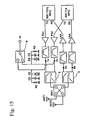
- the conventional power control circuit for wireless LAN comprises a coupler between a power amplifier PA1 and a diplexer 3 for transmission signals, a detection signal from the coupler being rectified by a detector comprising a detection diode D2 and a smoothing circuit C2, R2, to control an output signal of RFIC based on the resultant detection voltage.
- This power control circuit requires a coupler, and a detector comprising a detection diode and a smoothing circuit for both of PA1 in a 2.4-GHz band and PA2 in a 5-GHz band, as well as an analog switch 6 for selecting detection voltage terminals for the 2.4-GHz band and the 5-GHz band. Accordingly, it needs many parts, resulting in difficulty in reducing the size of an communications apparatus.
- Japanese Patent 3,371,887 proposes a circuit comprising a coupler 7 connected to a common end of a diplexer 3, as shown in Fig. 16.
- This circuit has parts whose number is reduced to 1/2 or less of that in the detection circuit shown in Fig. 15, and can monitor an output power at a position near an antenna, resulting in improved detection precision.
- both transmission powers in a 2.4-GHz band and a 5-GHz band should be detected in the circuit shown in Fig. 16, it is extremely difficult to keep the relation between output power and detection voltage constant, when the coupling degree of the coupler largely depends on a frequency.
- a detection diode should be disposed to detect transmission powers in both 2.4-GHz and 5-GHz bands, but it generates harmonic signals due to its detection distortion.
- the harmonic signals mainly having frequencies 2 or 3 times those of the transmission signals are reflected toward the coupler, so that most of them are radiated from the antenna via the coupler.
- laminated couplers With respect to the frequency dependency of the coupling degree of the coupler, for instance, small, low-loss, laminated couplers generally have coupling degrees of -15 dB and -10 dB, respectively, in a 2.4-GHz band and a 5-GHz band, this difference directly affecting their detection voltages.
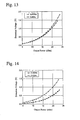
- the detection voltage is +0.5 V at 2.45 GHz and +1 V at 5.4 GHz, for instance, when there is an output of +20 dBm at an antenna end as shown in Fig. 14.
- Such variations of the detection voltage depending on the frequency should be reduced to enable the TPC function.
- an object of the present invention is to provide a high-frequency circuit with reduced harmonic signals generated by a detection diode, small variations of a detection voltage in pluralities of frequencies, and a small number of parts.
- Another object of the present invention is to provide a wireless LAN communications apparatus comprising such high-frequency circuit.
- the first high-frequency circuit of the present invention comprises a coupler having a primary line having input and output ends for a transmission signal and a secondary line, a detector comprising a detection diode for detecting a transmission power of a high-frequency signal sent from the secondary line of the coupler, and a harmonics-suppressing circuit disposed between the secondary line of the coupler and the detection diode.
- the harmonics-suppressing circuit is preferably a low-pass filter circuit or a notch filter circuit constituted by one or more transmission lines and one or more capacitors, or an attenuator circuit constituted by one or more resistors.
- the harmonics-suppressing circuit has conventionally been disposed in a main line, through which a transmission signal and a receiving signal pass, it is disposed between the coupler and the detection diode in the present invention. This makes it possible to drastically reduce the loss of the main line, through which a transmission signal and a receiving signal pass, resulting in higher quality and lower power consumption of communications.
- the low-pass filter circuit or the notch filter circuit constituting the harmonics-suppressing circuit in the high-frequency circuit of the present invention preferably has an attenuation pole adjusted to 2 or 3 times the passband frequency, without attenuation at the passband frequency. This makes it possible to reduce only harmonic signals while keeping the detection voltage constant.
- the low-pass filter circuit and the notch filter circuit are effective when a signal being detected has a relatively narrow passband.
- the attenuator circuit constituted by one or more resistors is more preferable than the low-pass filter circuit and the notch filter circuit, because the attenuator can attenuate a signal in a wide band.
- the first and second frequency bands are a 2.4-GHz band and a 5-GHz band, respectively
- detection in the 5-GHz band is insufficient in the low-pass filter circuit and the notch filter circuit, because a second-harmonic signal in the first frequency band is substantially 5 GHz.
- the attenuator circuit attenuates not only a detected signal from the coupler but also reflected waves of harmonic signals generated by the detection diode.
- the use of the attenuator circuit makes it necessary for the coupler to have a large coupling degree to keep the detection voltage constant, it is advantageous in providing sufficient attenuation in a broad band.
- the harmonics-suppressing circuit is preferably a notch filter constituted by an inductor, a diode, a capacitor, a resistor and a power-supplying terminal for attenuating frequencies 2 or 3 times those of transmission signals in a first frequency band (for instance, 2.4-GHz band) and a second frequency band (for instance, 5-GHz band), and it is preferable to use a variable notch filter having a variable resonance frequency attenuated by voltage applied to the power-supplying terminal.
- a first frequency band for instance, 2.4-GHz band
- a second frequency band for instance, 5-GHz band
- the attenuation pole By ON/OFF of the power-supplying terminal of the variable notch filter, the attenuation pole can be set to a frequency 2 times that of the first transmission signal when a transmission signal in the first frequency band is sent to the antenna, and to the frequency of a second harmonic of the second transmission signal when a transmission signal in the second frequency band is sent to the antenna.
- the second harmonics can be reduced by one filter.
- a matching circuit constituted by a shunt inductor connected to the coupling line of the coupler, and/or a matching circuit constituted by a shunt inductor and a phase circuit connected between the coupling line of the coupler and the detection diode are preferably disposed between the secondary line of the coupler and the harmonics-suppressing circuit.
- This matching circuit is preferably adjusted such that impedance matching is obtained between the coupling line of the coupler and the detection diode in a first frequency band (for instance, 2.4-GHz band). This increases the detection voltage in a 2.4-GHz band, in which the coupler has a small coupling degree and the detection voltage is small, thereby reducing differences from the detection voltage in a 5-GHz band.
- This matching circuit can separately adjust impedance matching in an amplitude direction by the shunt inductor and impedance matching in a phase direction by the phase circuit on a Smith chart. As a result, impedance matching can be easily adjusted between the coupling line of the coupler and the detection diode in a 2.4-GHz band.
- the high-frequency circuit of the present invention preferably comprises a switch circuit for switching a transmission signal and a receiving signal, which comprises one or more antenna ends for inputting and outputting a transmission signal and a receiving signal, one or more transmission ends for inputting a transmission signal, and one or more receiving ends for outputting a receiving signal, the transmission end of the switch circuit being connected to the primary line of the coupler.
- this circuit structure can provide a dual-band RF front-end circuit applicable to the communications systems of IEEE802.11a, IEEE802.11b and IEEE802.11g.
- This circuit structure can also provide a single-band RF front-end circuit usable in a 2.4 GHz band or a 5 GHz band.
- the wireless communications apparatus of the present invention comprises the above-described high-frequency circuit.
- Fig. 1 shows a high-frequency circuit according to one embodiment of the present invention.
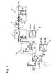
- This high-frequency circuit comprises a diplexer 3, a coupler 2, a detector 4 comprising a detection diode D 1 and a smoothing circuit 4', and a harmonics-suppressing circuit 1 disposed between the coupler 2 and the detection diode D1.
- the diplexer 3 is constituted by a combination of a low-pass filter and a high-pass filter, which are constituted, for instance, by LC circuits.
- the coupler 2 is constituted by a primary line L3, a secondary line L2 and a resistor R1.
- a coupling line CL on the side of the secondary line L2 of the coupler 2 is connected to the harmonics-suppressing circuit 1 and the detector 4 in series.
- the detection diode D 1 in the detector 4 has an anode terminal 1g connected to the harmonics-suppressing circuit 1, and a cathode terminal 1h connected to the smoothing circuit 4'.
- a transmission signal in a 2.4-GHz band (IEEE802.11b) and a transmission signal in a 5-GHz band (IEEE802.11a) are input to the input ends 1a and 1b of the diplexer 3, and transmission signals sent from the diplexer 3 to the antenna are input to the input end 1e of the coupler 2 and output from the output end 1c of the coupler 2. Because the primary line L3 and the secondary line L2 are coupled at high frequencies, part of the transmission signal is output to the coupling end 1f of the coupling line CL.
- a high-frequency signal passing through the coupler 2 and the harmonics-suppressing circuit 1 is input to the detection diode D1, and only a high-frequency signal exceeding the forward voltage of the detection diode D1 is transmitted to the cathode terminal 1h, converted to DC by the smoothing circuit 4', and output to the detection terminal 1d as a plus DC voltage.
- This detection signal is fed back to a transmission power amplifier via an RFIC circuit, etc. for use as a control.
- Harmonic signals generated in rectification by the detection diode D 1 are reflected and radiated through the antenna via the coupler 2.
- the harmonics-suppressing circuit 1 is constituted by a ⁇ -type low-pass filter having an attenuation pole, for instance, in a 10-GHz band, a second harmonic wave of the 5-GHz band.
- the attenuation pole may be in a third harmonic band of a 2.4-GHz band or in a second or third harmonic band of a 5-GHz band, depending on the circuit structure.
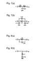
- Other examples of the harmonics-suppressing circuit 1 are a low-pass filter constituted by an LC circuit as shown in Figs.
- the low-pass filter provides large attenuation at frequencies exceeding the attenuation pole, it is not suitable for miniaturization because it needs large numbers of elements.
- the notch filter provides small attenuation at frequencies exceeding the attenuation pole, it easily achieves miniaturization because of small numbers of elements.
- the connection of the harmonics-suppressing circuit 1 to the anode of the detection diode D 1 makes it possible to detect a positive detection voltage.
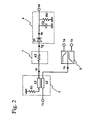
- Fig. 2 shows an example of the harmonics-suppressing circuit 1, which is constituted by an attenuator AT.
- the attenuator AT comprises a resistor for providing voltage drop to reduce the intensity of a high-frequency signal.
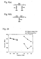
- Figs. 9(a) and 9(b) show specific examples of attenuators constituted by pluralities of resistors.
- an attenuator constituted by pluralities of resistors can provide higher attenuation than an attenuator of one resistor in a broad band, although the former is not suitable for miniaturization.
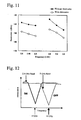
- the characteristic values (dBm) of second harmonics generated in a 2.4-GHz band and a 5-GHz band were measured.
- the results are shown in Figs. 10 and 11.
- Figs. 10 and 11 there are harmonics-suppressing effects of 10 dB or more except in the 2.4-GHz band in Fig. 10. Why an improved harmonics-suppressing effect is not obtained by the low-pass filter in the 2.4-GHz band appears to be due to the fact that the attenuation pole of the low-pass filter is set at 10 GHz.
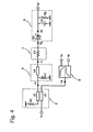
- Fig. 3 shows an example of high-frequency circuits, in which a harmonics-suppressing circuit 1 is constituted by a variable notch filter.
- the variable notch filter VNF is constituted by a transmission line or inductor L6, a choke coil L7, a capacitor C1, a diode switch D5, and a resistor R1.
- the transmission line L6, the diode D5 and the capacitor C 1 constitute a series resonance circuit, whose resonance frequency varies by ON/OFF of the diode D5. That is, it is usual that the diode is nearly short-circuited in an ON state, while it has a capacitance of 0.1-1.0 pF in an OFF state.
- a series resonance circuit is formed by L6 and C 1 in an ON state, and by L6, C 1 and the capacitance of the diode D5 in an OFF state.
- the attenuation pole of the resonance circuit can be changed by ON/OFF of the diode D5.
- variable notch filter VNF has an attenuation pole at a frequency of about 5 GHz, 2 times the frequency (2.4 GHz) of the first transmission signal when the diode D5 is in an ON state, and an attenuation pole at a frequency of about 10 GHz, 2 times the frequency (5 GHz) of the second transmission signal when the diode D5 is in an OFF state. Because the resonance frequencies at ON and OFF of the diode D5 can be arbitrarily adjusted by a combination of L6 and C1, the attenuation pole can also be set at the frequency of a third harmonic.
- DC current should be caused to flow through the diode D5 by applying voltage of about 0.5 V or more to the diode D5, and a choke coil L7 is needed for this DC current.
- the choke coil L7 is preferably 2 nH or more such that it has large impedance to signals in a 2.4 GHz band and a 5-GHz band.
- a choke coil L7 is 5.6 nH.
- a resistor R1 is disposed between the anode of the diode D5 and a power-supplying terminal V1, to limit electric current flowing through the diode D5.
- the resistor R1 is 2 k ⁇ .
- Fig. 4 shows a high-frequency circuit according to a still further embodiment of the present invention.
- This high-frequency circuit comprises a matching circuit 5 between the secondary line L2 of the coupler 2 and the harmonics-suppressing circuit 1.
- the matching circuit 5 is constituted by a shunt inductor L 1 and a phase circuit L4, a coupling signal being input from a coupling end 1f, and output to a detection diode D 1 via an attenuator AT.
- the constants of the shunt inductor L 1 and the phase circuit L4 are set to provide matching between the impedance of the coupling end 1f and the impedance of the coupling end 1i on the side of the detection diode D1 in a 2.4-GHz band.
- the matching circuit 5 can separately adjust impedance matching in an amplitude direction by the shunt inductor L1, and impedance matching in a phase direction by the phase circuit L4 on a Smith chart. Accordingly, impedance matching can be easily adjusted between the coupling end and the detection diode D 1 in a 2.4-GHz band. This can increase detection voltage even in a 2.4-GHz band in which the conventional circuit shown in Fig. 13 has a small coupling degree of the coupler and a small detection voltage, so that the difference from the detection voltage in a 5-GHz band can be reduced.
- Fig. 13 shows the relation between output power and detection voltage in the high-frequency circuit shown in Fig. 4. Compared with the conventional circuit shown in Fig. 14, the difference between the detection voltage in a 2.4-GHz band and the detection voltage in a 5-GHz band is much smaller.
- the harmonics-suppressing circuit 1 reduces harmonics, and the matching circuit 5 suppresses the variations of the coupling degree and the detection voltage, which depend on a frequency.
- a matching circuit 5 comprises both shunt inductor L1 and phase circuit L4, although modifications are possible depending on impedance matching between a coupling end 1f and the detection diode D1.
- the shunt inductor L1 or the phase circuit L4 may be used alone as the matching circuit 5 to achieve both impedance matching and miniaturization.
- Fig. 5 shows a high-frequency circuit according to a further embodiment of the present invention.
- This high-frequency circuit comprises a dual-pole, dual-throw (DPDT) switch circuit 8 for switching a transmission signal and a receiving signal, which has at least two multi-band antenna ends 5a, 5b capable of transmitting and receiving signals in a 2.4-GHz band and a 5-GHz band, a transmission end 1c for inputting transmission signals in a 2.4-GHz band and a 5-GHz band, and a receiving end 5c for outputting receiving signals in a 2.4-GHz band and a 5-GHz band.
- DPDT dual-pole, dual-throw
- the receiving end 5c of the switch circuit 8 is connected to a receiving diplexer 5 for dividing the receiving signals in a 2.4-GHz band and a 5-GHz band, and the transmission end 1c of the switch circuit 8 is connected to an output end of a coupler 2 in the same high-frequency circuit as shown in Fig. 4.
- the circuit structure downstream of the input ends 1a, 1b of the transmitting diplexer 3, and the circuit structure downstream of the output ends 5d, 5e of the receiving diplexer 5 are the same as shown in Fig. 15.
- This circuit structure provides an RF front-end circuit applicable to multi-band communications systems of IEEE802.11a, IEEE802.11b and IEEE802.11g.
- This high-frequency circuit provides small detection voltage variations depending on frequency, and achieves miniaturization due to a small number of parts. Thus, it is optimum for a multi-band communications apparatus of IEEE802.11h having a TPC function.
- Fig. 5 shows the transmission end 1c connected to the high-frequency circuit shown in Fig. 4, the same effects can be obtained by connecting the transmission end 1c to any one of the high-frequency circuits shown in Figs. 1-3.
- the present invention is not restricted thereto.
- a communications system comprising a single-pole, dual-throw (SPDT) switch circuit 9 for switching an antenna end 5a, a transmission end 1c for inputting a transmission signal from a power amplifier, and a receiving end 5c for outputting a receiving signal to a low-noise amplifier may be disposed, such that a transmission signal and a receiving signal in one band can be switched.
- SPDT single-pole, dual-throw
- This communications system can also provide the effects of the present invention, because the transmission end 1c is connected to the output end of the coupler 2 in the high-frequency circuit shown in Fig. 4.
- the high-frequency circuit of the present invention has a detection function for two transmission lines, thereby reducing harmonics reflected from the detection diode. Also, a matching circuit provides the high-frequency circuit with small detection voltage difference in two frequencies, and miniaturization due to a small number of parts. The use of such high-frequency circuit provides a communications apparatus for wireless LAN, etc., which is optimum for communications systems ofIEEE802.11h having a TPC function.
Landscapes
- Engineering & Computer Science (AREA)
- Power Engineering (AREA)
- Physics & Mathematics (AREA)
- General Physics & Mathematics (AREA)
- Transmitters (AREA)
- Transceivers (AREA)
Abstract
Description
- The present invention relates to a high-frequency circuit handling at least two communications systems and having a function to detect a transmission power, and an apparatus comprising such high-frequency circuit for wireless communications among electronic appliances.
- Data communications by wireless LAN (local area network) according to IEEE802.11 are now widely used. They are used as signal-transmitting means in place of personal computers (PCs); PC peripherals such as printers, hard disk drives, broadband rooters, etc.; electronic appliances such as facsimiles, refrigerators, standard-definition televisions (SDTVs), high-definition televisions (HDTVs), digital cameras, digital video recorders, cell phones, etc.; and wired communications of automobiles and aircrafts, and wireless data transmission is conducted among these electronic appliances.
- There are IEEE802.11a, IEEE802.11b and IEEE802.11g as the standards of wireless LAN. IEEE802.11a is adapted to high-speed data communications of 54 Mbps at maximum in a frequency band of 5 GHz, using an orthogonal frequency division multiples (OFDM) system. IEEE802.11b is adapted to high-speed communications of 5.5 Mbps and 11 Mbps in an industrial, scientific and medical (ISM) band of 2.4 GHz that can be freely used without wireless license, using a direct sequence spread spectrum (DSSS) system. IEEE802.11g is adapted to high-speed data communications of 54 Mbps at maximum in a 2.4-GHz band like IEEE802.11b, using the OFDM system.
-
WO 03/092997 diplexer 3 disposed between one port of the high-frequency switch SW1 and the transmission circuits, and adiplexer 5 disposed between another port of the high-frequency switch SW1 and the receiving circuits, thereby being able to conduct diversity reception. - There is IEEE802.11h, a communications system making wireless LAN usable in Europe. This requires a transmission power control (TPC) function to reduce a transmission power, when good transmission can be obtained even though the transmission power is suppressed, for instance, because terminals are close to base stations. For this purpose, the output power should be able to be controlled more precisely than the conventional wireless LAN.
- As shown in Fig. 15 of
WO 03/092997 diplexer 3 for transmission signals, a detection signal from the coupler being rectified by a detector comprising a detection diode D2 and a smoothing circuit C2, R2, to control an output signal of RFIC based on the resultant detection voltage. This power control circuit requires a coupler, and a detector comprising a detection diode and a smoothing circuit for both of PA1 in a 2.4-GHz band and PA2 in a 5-GHz band, as well as ananalog switch 6 for selecting detection voltage terminals for the 2.4-GHz band and the 5-GHz band. Accordingly, it needs many parts, resulting in difficulty in reducing the size of an communications apparatus. - To solve this problem,
Japanese Patent 3,371,887 coupler 7 connected to a common end of adiplexer 3, as shown in Fig. 16. This circuit has parts whose number is reduced to 1/2 or less of that in the detection circuit shown in Fig. 15, and can monitor an output power at a position near an antenna, resulting in improved detection precision. However, because both transmission powers in a 2.4-GHz band and a 5-GHz band should be detected in the circuit shown in Fig. 16, it is extremely difficult to keep the relation between output power and detection voltage constant, when the coupling degree of the coupler largely depends on a frequency. - A detection diode (Schottky diode) should be disposed to detect transmission powers in both 2.4-GHz and 5-GHz bands, but it generates harmonic signals due to its detection distortion. The harmonic signals mainly having
frequencies - Accordingly, an object of the present invention is to provide a high-frequency circuit with reduced harmonic signals generated by a detection diode, small variations of a detection voltage in pluralities of frequencies, and a small number of parts.
- Another object of the present invention is to provide a wireless LAN communications apparatus comprising such high-frequency circuit.
- The first high-frequency circuit of the present invention comprises a coupler having a primary line having input and output ends for a transmission signal and a secondary line, a detector comprising a detection diode for detecting a transmission power of a high-frequency signal sent from the secondary line of the coupler, and a harmonics-suppressing circuit disposed between the secondary line of the coupler and the detection diode.
- The second high-frequency circuit of the present invention for use in a dual-band wireless communications apparatus selectively using first and second frequency bands comprises a diplexer connected to the output side of a power amplifier for sending either one of transmission signals in the first and second frequency bands to an antenna, a coupler having a primary line connected to a common end of the diplexer and a secondary line, a detector comprising a detection diode for detecting a transmission power of a high-frequency signal sent from the secondary line of the coupler, and a harmonics-suppressing circuit disposed between the secondary line of the coupler and the detection diode.
- The harmonics-suppressing circuit is preferably a low-pass filter circuit or a notch filter circuit constituted by one or more transmission lines and one or more capacitors, or an attenuator circuit constituted by one or more resistors. Although the harmonics-suppressing circuit has conventionally been disposed in a main line, through which a transmission signal and a receiving signal pass, it is disposed between the coupler and the detection diode in the present invention. This makes it possible to drastically reduce the loss of the main line, through which a transmission signal and a receiving signal pass, resulting in higher quality and lower power consumption of communications.
- The low-pass filter circuit or the notch filter circuit constituting the harmonics-suppressing circuit in the high-frequency circuit of the present invention preferably has an attenuation pole adjusted to 2 or 3 times the passband frequency, without attenuation at the passband frequency. This makes it possible to reduce only harmonic signals while keeping the detection voltage constant.
- The low-pass filter circuit and the notch filter circuit are effective when a signal being detected has a relatively narrow passband.
- When used in a dual-band wireless communications apparatus selectively using first and second frequency bands, the attenuator circuit constituted by one or more resistors is more preferable than the low-pass filter circuit and the notch filter circuit, because the attenuator can attenuate a signal in a wide band. For instance, when the first and second frequency bands are a 2.4-GHz band and a 5-GHz band, respectively, detection in the 5-GHz band is insufficient in the low-pass filter circuit and the notch filter circuit, because a second-harmonic signal in the first frequency band is substantially 5 GHz. On the other hand, the attenuator circuit attenuates not only a detected signal from the coupler but also reflected waves of harmonic signals generated by the detection diode. Although the use of the attenuator circuit makes it necessary for the coupler to have a large coupling degree to keep the detection voltage constant, it is advantageous in providing sufficient attenuation in a broad band.
- The harmonics-suppressing circuit is preferably a notch filter constituted by an inductor, a diode, a capacitor, a resistor and a power-supplying terminal for attenuating
frequencies frequency 2 times that of the first transmission signal when a transmission signal in the first frequency band is sent to the antenna, and to the frequency of a second harmonic of the second transmission signal when a transmission signal in the second frequency band is sent to the antenna. Thus, by changing the attenuation poles in both bands, the second harmonics can be reduced by one filter. - A matching circuit constituted by a shunt inductor connected to the coupling line of the coupler, and/or a matching circuit constituted by a shunt inductor and a phase circuit connected between the coupling line of the coupler and the detection diode are preferably disposed between the secondary line of the coupler and the harmonics-suppressing circuit. This matching circuit is preferably adjusted such that impedance matching is obtained between the coupling line of the coupler and the detection diode in a first frequency band (for instance, 2.4-GHz band). This increases the detection voltage in a 2.4-GHz band, in which the coupler has a small coupling degree and the detection voltage is small, thereby reducing differences from the detection voltage in a 5-GHz band. This matching circuit can separately adjust impedance matching in an amplitude direction by the shunt inductor and impedance matching in a phase direction by the phase circuit on a Smith chart. As a result, impedance matching can be easily adjusted between the coupling line of the coupler and the detection diode in a 2.4-GHz band.
- The high-frequency circuit of the present invention preferably comprises a switch circuit for switching a transmission signal and a receiving signal, which comprises one or more antenna ends for inputting and outputting a transmission signal and a receiving signal, one or more transmission ends for inputting a transmission signal, and one or more receiving ends for outputting a receiving signal, the transmission end of the switch circuit being connected to the primary line of the coupler. When the first frequency band is a 2.4-GHz band, and the second frequency band is a 5-GHz band, this circuit structure can provide a dual-band RF front-end circuit applicable to the communications systems of IEEE802.11a, IEEE802.11b and IEEE802.11g. This circuit structure can also provide a single-band RF front-end circuit usable in a 2.4 GHz band or a 5 GHz band.
- The wireless communications apparatus of the present invention comprises the above-described high-frequency circuit.
-
- Fig. 1 is a block diagram showing a high-frequency circuit comprising a harmonics-suppressing circuit according to one embodiment of the present invention.
- Fig. 2 is a block diagram showing a high-frequency circuit comprising a harmonics-suppressing circuit according to another embodiment of the present invention.
- Fig. 3 is a block diagram showing a high-frequency circuit comprising a harmonics-suppressing circuit according to a further embodiment of the present invention.
- Fig. 4 is a block diagram showing a high-frequency circuit comprising a harmonics-suppressing circuit and a matching circuit according to a still further embodiment of the present invention.
- Fig. 5 is a block diagram showing a high-frequency circuit according to a still further embodiment of the present invention, which is obtained by adding a switch circuit, a diplexer circuit, etc. to the high-frequency circuit of Fig. 4.
- Fig. 6 is a block diagram showing a high-frequency circuit comprising a harmonics-suppressing circuit according to a still further embodiment of the present invention.
- Fig. 7 is a view showing one example of low-pass filters used in the harmonics-suppressing circuit of the present invention.
- Fig. 8 is a view showing one example of notch filters used in the harmonics-suppressing circuit of the present invention.
- Fig. 9 is a view showing one example of attenuators used in the harmonics-suppressing circuit of the present invention.
- Fig. 10 is a graph showing the harmonics-attenuating characteristics of the harmonics-suppressing circuit of Fig. 1.
- Fig. 11 is a graph showing the harmonics-attenuating characteristics of the harmonics-suppressing circuit of Fig. 2.
- Fig. 12 is a graph showing the harmonics-attenuating characteristics of the harmonics-suppressing circuit of Fig. 3.
- Fig. 13 is a graph showing the relation between output power and detection voltage in the high-frequency circuit of Fig. 4.
- Fig. 14 is a graph showing the relation between output power and detection voltage in a conventional high-frequency circuit.
- Fig. 15 is a block diagram showing one example of high-frequency circuits having conventional detection functions.
- Fig. 16 is a block diagram showing another example of high-frequency circuits having conventional detection functions.
- Fig. 1 shows a high-frequency circuit according to one embodiment of the present invention. This high-frequency circuit comprises a
diplexer 3, acoupler 2, adetector 4 comprising a detection diode D 1 and a smoothing circuit 4', and a harmonics-suppressing circuit 1 disposed between thecoupler 2 and the detection diode D1. Thediplexer 3 is constituted by a combination of a low-pass filter and a high-pass filter, which are constituted, for instance, by LC circuits. Thecoupler 2 is constituted by a primary line L3, a secondary line L2 and a resistor R1. A coupling line CL on the side of the secondary line L2 of thecoupler 2 is connected to the harmonics-suppressing circuit 1 and thedetector 4 in series. The detection diode D 1 in thedetector 4 has ananode terminal 1g connected to the harmonics-suppressing circuit 1, and acathode terminal 1h connected to the smoothing circuit 4'. - A transmission signal in a 2.4-GHz band (IEEE802.11b) and a transmission signal in a 5-GHz band (IEEE802.11a) are input to the input ends 1a and 1b of the
diplexer 3, and transmission signals sent from thediplexer 3 to the antenna are input to theinput end 1e of thecoupler 2 and output from theoutput end 1c of thecoupler 2. Because the primary line L3 and the secondary line L2 are coupled at high frequencies, part of the transmission signal is output to thecoupling end 1f of the coupling line CL. - A high-frequency signal passing through the
coupler 2 and the harmonics-suppressing circuit 1 is input to the detection diode D1, and only a high-frequency signal exceeding the forward voltage of the detection diode D1 is transmitted to thecathode terminal 1h, converted to DC by the smoothing circuit 4', and output to thedetection terminal 1d as a plus DC voltage. This detection signal is fed back to a transmission power amplifier via an RFIC circuit, etc. for use as a control. - Harmonic signals generated in rectification by the detection diode D 1 are reflected and radiated through the antenna via the
coupler 2. Provided to prevent this is the harmonics-suppressing circuit 1 as shown in Fig. 1. The harmonics-suppressing circuit 1 is constituted by a π-type low-pass filter having an attenuation pole, for instance, in a 10-GHz band, a second harmonic wave of the 5-GHz band. The attenuation pole may be in a third harmonic band of a 2.4-GHz band or in a second or third harmonic band of a 5-GHz band, depending on the circuit structure. Other examples of the harmonics-suppressing circuit 1 are a low-pass filter constituted by an LC circuit as shown in Figs. 7(a) and 7(b), and a notch filter as shown in Figs. 8(a) and 8(b). Although the low-pass filter provides large attenuation at frequencies exceeding the attenuation pole, it is not suitable for miniaturization because it needs large numbers of elements. Although the notch filter provides small attenuation at frequencies exceeding the attenuation pole, it easily achieves miniaturization because of small numbers of elements. The connection of the harmonics-suppressing circuit 1 to the anode of the detection diode D 1 makes it possible to detect a positive detection voltage. - Fig. 2 shows an example of the harmonics-suppressing circuit 1, which is constituted by an attenuator AT. The attenuator AT comprises a resistor for providing voltage drop to reduce the intensity of a high-frequency signal. Figs. 9(a) and 9(b) show specific examples of attenuators constituted by pluralities of resistors. In general, an attenuator constituted by pluralities of resistors can provide higher attenuation than an attenuator of one resistor in a broad band, although the former is not suitable for miniaturization.
- With respect to the harmonics-suppressing circuit 1 constituted by a π-type low-pass filter as shown in Fig. 1 and the harmonics-suppressing circuit 1 constituted by the attenuator AT as shown in Fig. 2, the characteristic values (dBm) of second harmonics generated in a 2.4-GHz band and a 5-GHz band were measured. The results are shown in Figs. 10 and 11. As is clear from Figs. 10 and 11, there are harmonics-suppressing effects of 10 dB or more except in the 2.4-GHz band in Fig. 10. Why an improved harmonics-suppressing effect is not obtained by the low-pass filter in the 2.4-GHz band appears to be due to the fact that the attenuation pole of the low-pass filter is set at 10 GHz.
- Fig. 3 shows an example of high-frequency circuits, in which a harmonics-suppressing circuit 1 is constituted by a variable notch filter. The variable notch filter VNF is constituted by a transmission line or inductor L6, a choke coil L7, a capacitor C1, a diode switch D5, and a resistor R1. The transmission line L6, the diode D5 and the capacitor C 1 constitute a series resonance circuit, whose resonance frequency varies by ON/OFF of the diode D5. That is, it is usual that the diode is nearly short-circuited in an ON state, while it has a capacitance of 0.1-1.0 pF in an OFF state. Accordingly, a series resonance circuit is formed by L6 and C 1 in an ON state, and by L6, C 1 and the capacitance of the diode D5 in an OFF state. Thus, the attenuation pole of the resonance circuit can be changed by ON/OFF of the diode D5.
- The characteristics of the variable notch filter VNF shown in Fig. 3 are shown in Fig. 12. The variable notch filter VNF has an attenuation pole at a frequency of about 5 GHz, 2 times the frequency (2.4 GHz) of the first transmission signal when the diode D5 is in an ON state, and an attenuation pole at a frequency of about 10 GHz, 2 times the frequency (5 GHz) of the second transmission signal when the diode D5 is in an OFF state. Because the resonance frequencies at ON and OFF of the diode D5 can be arbitrarily adjusted by a combination of L6 and C1, the attenuation pole can also be set at the frequency of a third harmonic. To turn the diode D5 to an ON state, DC current should be caused to flow through the diode D5 by applying voltage of about 0.5 V or more to the diode D5, and a choke coil L7 is needed for this DC current. The choke coil L7 is preferably 2 nH or more such that it has large impedance to signals in a 2.4 GHz band and a 5-GHz band. In this embodiment, a choke coil L7 is 5.6 nH. A resistor R1 is disposed between the anode of the diode D5 and a power-supplying terminal V1, to limit electric current flowing through the diode D5. In this embodiment, the resistor R1 is 2 kΩ.
- Fig. 4 shows a high-frequency circuit according to a still further embodiment of the present invention. This high-frequency circuit comprises a
matching circuit 5 between the secondary line L2 of thecoupler 2 and the harmonics-suppressing circuit 1. Thematching circuit 5 is constituted by a shunt inductor L 1 and a phase circuit L4, a coupling signal being input from acoupling end 1f, and output to a detection diode D 1 via an attenuator AT. The constants of the shunt inductor L 1 and the phase circuit L4 are set to provide matching between the impedance of thecoupling end 1f and the impedance of thecoupling end 1i on the side of the detection diode D1 in a 2.4-GHz band. Thematching circuit 5 can separately adjust impedance matching in an amplitude direction by the shunt inductor L1, and impedance matching in a phase direction by the phase circuit L4 on a Smith chart. Accordingly, impedance matching can be easily adjusted between the coupling end and the detection diode D 1 in a 2.4-GHz band. This can increase detection voltage even in a 2.4-GHz band in which the conventional circuit shown in Fig. 13 has a small coupling degree of the coupler and a small detection voltage, so that the difference from the detection voltage in a 5-GHz band can be reduced. - Fig. 13 shows the relation between output power and detection voltage in the high-frequency circuit shown in Fig. 4. Compared with the conventional circuit shown in Fig. 14, the difference between the detection voltage in a 2.4-GHz band and the detection voltage in a 5-GHz band is much smaller.
- In the embodiment shown in Fig. 4, the harmonics-suppressing circuit 1 reduces harmonics, and the
matching circuit 5 suppresses the variations of the coupling degree and the detection voltage, which depend on a frequency. - In the embodiment shown in Fig. 4, a
matching circuit 5 comprises both shunt inductor L1 and phase circuit L4, although modifications are possible depending on impedance matching between acoupling end 1f and the detection diode D1. For instance, the shunt inductor L1 or the phase circuit L4 may be used alone as thematching circuit 5 to achieve both impedance matching and miniaturization. - Fig. 5 shows a high-frequency circuit according to a further embodiment of the present invention. This high-frequency circuit comprises a dual-pole, dual-throw (DPDT) switch circuit 8 for switching a transmission signal and a receiving signal, which has at least two multi-band antenna ends 5a, 5b capable of transmitting and receiving signals in a 2.4-GHz band and a 5-GHz band, a
transmission end 1c for inputting transmission signals in a 2.4-GHz band and a 5-GHz band, and a receivingend 5c for outputting receiving signals in a 2.4-GHz band and a 5-GHz band. The receivingend 5c of the switch circuit 8 is connected to a receivingdiplexer 5 for dividing the receiving signals in a 2.4-GHz band and a 5-GHz band, and thetransmission end 1c of the switch circuit 8 is connected to an output end of acoupler 2 in the same high-frequency circuit as shown in Fig. 4. The circuit structure downstream of the input ends 1a, 1b of the transmittingdiplexer 3, and the circuit structure downstream of the output ends 5d, 5e of the receivingdiplexer 5 are the same as shown in Fig. 15. - This circuit structure provides an RF front-end circuit applicable to multi-band communications systems of IEEE802.11a, IEEE802.11b and IEEE802.11g. This high-frequency circuit provides small detection voltage variations depending on frequency, and achieves miniaturization due to a small number of parts. Thus, it is optimum for a multi-band communications apparatus of IEEE802.11h having a TPC function. Although Fig. 5 shows the
transmission end 1c connected to the high-frequency circuit shown in Fig. 4, the same effects can be obtained by connecting thetransmission end 1c to any one of the high-frequency circuits shown in Figs. 1-3. - Although the high-frequency circuits capable of handling two bands at 2.4 and 5 GHz have been explained above, the present invention is not restricted thereto. For instance, as shown in Fig. 6, it is applicable to a communications system comprising a single-pole, dual-throw (SPDT)
switch circuit 9 for switching anantenna end 5a, atransmission end 1c for inputting a transmission signal from a power amplifier, and a receivingend 5c for outputting a receiving signal to a low-noise amplifier may be disposed, such that a transmission signal and a receiving signal in one band can be switched. This communications system can also provide the effects of the present invention, because thetransmission end 1c is connected to the output end of thecoupler 2 in the high-frequency circuit shown in Fig. 4. - Because the harmonics-suppressing circuit is connected to the secondary line of the coupler, the high-frequency circuit of the present invention has a detection function for two transmission lines, thereby reducing harmonics reflected from the detection diode. Also, a matching circuit provides the high-frequency circuit with small detection voltage difference in two frequencies, and miniaturization due to a small number of parts. The use of such high-frequency circuit provides a communications apparatus for wireless LAN, etc., which is optimum for communications systems ofIEEE802.11h having a TPC function.
Claims (7)
- A high-frequency circuit comprising a coupler having a primary line having input and output ends for a transmission signal and a secondary line, a detector comprising a detection diode for detecting a transmission power of a high-frequency signal sent from the secondary line of said coupler, and a harmonics-suppressing circuit disposed between the secondary line of said coupler and said detection diode.
- A high-frequency circuit for use in a dual-band wireless communications apparatus selectively using first and second frequency bands, comprising a diplexer connected to the output of a power amplifier for sending either one of transmission signals in said first and second frequency bands to an antenna, a coupler having a primary line connected to a common end of said diplexer and a secondary line, a detector comprising a detection diode for detecting a transmission power of a high-frequency signal sent from the secondary line of said coupler, and a harmonics-suppressing circuit disposed between the secondary line of said coupler and said detection diode.
- The circuit of claim 1 or 2, wherein said harmonics-suppressing circuit is a low-pass filter circuit or a notch filter circuit constituted by one or more transmission lines and one or more capacitors, or an attenuator circuit constituted by one or more resistors.
- The circuit of claim 3, wherein said notch filter comprises an inductor, a diode, a capacitor, a resistor and a power-supplying terminal, whereby a resonance frequency attenuated by voltage applied to said power-supplying terminal is variable.
- The circuit of any preceding claim, wherein a matching circuit constituted by a shunt inductor connected to the coupling line of said coupler, and/or a matching circuit constituted by a shunt inductor and a phase circuit connected between the coupling line of said coupler and said detection diode are disposed between the secondary line of said coupler and said harmonics-suppressing circuit.
- The circuit of any preceding claim, comprising a switch circuit for switching a transmission signal and a receiving signal, which comprises one or more antenna ends for inputting and outputting a transmission signal and a receiving signal, one or more transmission ends for inputting a transmission signal, and one or more receiving ends for outputting a receiving signal, said transmission end of said switch circuit being connected to the primary line of said coupler.
- A communications apparatus comprising the high-frequency circuit recited in any preceding claim.
Applications Claiming Priority (1)
| Application Number | Priority Date | Filing Date | Title |
|---|---|---|---|
| JP2005110867A JP2006295375A (en) | 2005-04-07 | 2005-04-07 | High frequency circuit and communication system using the same |
Publications (3)
| Publication Number | Publication Date |
|---|---|
| EP1710925A2 true EP1710925A2 (en) | 2006-10-11 |
| EP1710925A3 EP1710925A3 (en) | 2006-11-02 |
| EP1710925B1 EP1710925B1 (en) | 2020-08-05 |
Family
ID=36570638
Family Applications (1)
| Application Number | Title | Priority Date | Filing Date |
|---|---|---|---|
| EP06007063.8A Expired - Lifetime EP1710925B1 (en) | 2005-04-07 | 2006-04-03 | Multi-band high-frequency circuit |
Country Status (5)
| Country | Link |
|---|---|
| US (1) | US7705692B2 (en) |
| EP (1) | EP1710925B1 (en) |
| JP (1) | JP2006295375A (en) |
| CN (1) | CN1870555B (en) |
| TW (1) | TWI376889B (en) |
Cited By (2)
| Publication number | Priority date | Publication date | Assignee | Title |
|---|---|---|---|---|
| EP1768269A4 (en) * | 2004-06-30 | 2015-04-22 | Hitachi Metals Ltd | High frequency circuit, high frequency component, and multi-band communication apparatus |
| CN113691277A (en) * | 2021-09-26 | 2021-11-23 | 广东宽普科技有限公司 | High-frequency short-wave high-suppression communication circuit |
Families Citing this family (51)
| Publication number | Priority date | Publication date | Assignee | Title |
|---|---|---|---|---|
| US8744384B2 (en) | 2000-07-20 | 2014-06-03 | Blackberry Limited | Tunable microwave devices with auto-adjusting matching circuit |
| US9406444B2 (en) | 2005-11-14 | 2016-08-02 | Blackberry Limited | Thin film capacitors |
| US7711337B2 (en) | 2006-01-14 | 2010-05-04 | Paratek Microwave, Inc. | Adaptive impedance matching module (AIMM) control architectures |
| US7535312B2 (en) | 2006-11-08 | 2009-05-19 | Paratek Microwave, Inc. | Adaptive impedance matching apparatus, system and method with improved dynamic range |
| US7714676B2 (en) | 2006-11-08 | 2010-05-11 | Paratek Microwave, Inc. | Adaptive impedance matching apparatus, system and method |
| US10715209B2 (en) * | 2006-11-18 | 2020-07-14 | RF Micron, Inc. | Computing device for processing environmental sensed conditions |
| US20090102579A1 (en) * | 2006-12-29 | 2009-04-23 | Broadcom Corporation | Frequency division coupling circuit and applications thereof |
| DE102007003182B4 (en) * | 2007-01-22 | 2019-11-28 | Snaptrack Inc. | Electrical component |
| JP4927162B2 (en) * | 2007-03-29 | 2012-05-09 | 京セラ株式会社 | Portable radio |
| US7917104B2 (en) | 2007-04-23 | 2011-03-29 | Paratek Microwave, Inc. | Techniques for improved adaptive impedance matching |
| US8213886B2 (en) | 2007-05-07 | 2012-07-03 | Paratek Microwave, Inc. | Hybrid techniques for antenna retuning utilizing transmit and receive power information |
| TWI364195B (en) * | 2007-10-12 | 2012-05-11 | Filtering apparatus and method for dual-band sensing circuit | |
| US7991363B2 (en) | 2007-11-14 | 2011-08-02 | Paratek Microwave, Inc. | Tuning matching circuits for transmitter and receiver bands as a function of transmitter metrics |
| US20090131001A1 (en) * | 2007-11-16 | 2009-05-21 | James Breslin | Switch architecture |
| US8072285B2 (en) | 2008-09-24 | 2011-12-06 | Paratek Microwave, Inc. | Methods for tuning an adaptive impedance matching network with a look-up table |
| US8301091B2 (en) * | 2009-01-30 | 2012-10-30 | Avago Technologies General Ip (Singapore) Pte. Ltd. | Power detector for multi-band network access |
| US8208867B2 (en) * | 2009-04-09 | 2012-06-26 | Apple Inc. | Shared multiband antennas and antenna diversity circuitry for electronic devices |
| US8472888B2 (en) | 2009-08-25 | 2013-06-25 | Research In Motion Rf, Inc. | Method and apparatus for calibrating a communication device |
| US9026062B2 (en) | 2009-10-10 | 2015-05-05 | Blackberry Limited | Method and apparatus for managing operations of a communication device |
| US20110117869A1 (en) * | 2009-11-18 | 2011-05-19 | Ryan Woodings | Multiple band portable spectrum analyzer |
| US8803631B2 (en) | 2010-03-22 | 2014-08-12 | Blackberry Limited | Method and apparatus for adapting a variable impedance network |
| CN102948083B (en) | 2010-04-20 | 2015-05-27 | 黑莓有限公司 | Method and apparatus for managing interference in a communication device |
| US9948348B2 (en) | 2010-05-26 | 2018-04-17 | Skyworks Solutions, Inc. | High isolation switch with notch filter |
| US9379454B2 (en) * | 2010-11-08 | 2016-06-28 | Blackberry Limited | Method and apparatus for tuning antennas in a communication device |
| US8659496B1 (en) * | 2010-11-24 | 2014-02-25 | R.A. Miller Industries, Inc. | Heat sink for a high power antenna |
| US8712340B2 (en) | 2011-02-18 | 2014-04-29 | Blackberry Limited | Method and apparatus for radio antenna frequency tuning |
| US8655286B2 (en) | 2011-02-25 | 2014-02-18 | Blackberry Limited | Method and apparatus for tuning a communication device |
| US8626083B2 (en) | 2011-05-16 | 2014-01-07 | Blackberry Limited | Method and apparatus for tuning a communication device |
| US8594584B2 (en) | 2011-05-16 | 2013-11-26 | Blackberry Limited | Method and apparatus for tuning a communication device |
| US20130027273A1 (en) * | 2011-07-27 | 2013-01-31 | Tdk Corporation | Directional coupler and wireless communication device |
| WO2013022826A1 (en) | 2011-08-05 | 2013-02-14 | Research In Motion Rf, Inc. | Method and apparatus for band tuning in a communication device |
| US9065504B2 (en) * | 2011-10-28 | 2015-06-23 | Broadcom Corporation | Transmitter front end with programmable notch filter and methods for use therewith |
| US8948889B2 (en) | 2012-06-01 | 2015-02-03 | Blackberry Limited | Methods and apparatus for tuning circuit components of a communication device |
| US9853363B2 (en) | 2012-07-06 | 2017-12-26 | Blackberry Limited | Methods and apparatus to control mutual coupling between antennas |
| US9246223B2 (en) | 2012-07-17 | 2016-01-26 | Blackberry Limited | Antenna tuning for multiband operation |
| US9350405B2 (en) | 2012-07-19 | 2016-05-24 | Blackberry Limited | Method and apparatus for antenna tuning and power consumption management in a communication device |
| US9413066B2 (en) | 2012-07-19 | 2016-08-09 | Blackberry Limited | Method and apparatus for beam forming and antenna tuning in a communication device |
| US9362891B2 (en) | 2012-07-26 | 2016-06-07 | Blackberry Limited | Methods and apparatus for tuning a communication device |
| US10404295B2 (en) | 2012-12-21 | 2019-09-03 | Blackberry Limited | Method and apparatus for adjusting the timing of radio antenna tuning |
| US9374113B2 (en) | 2012-12-21 | 2016-06-21 | Blackberry Limited | Method and apparatus for adjusting the timing of radio antenna tuning |
| FR3004007A1 (en) * | 2013-03-29 | 2014-10-03 | St Microelectronics Tours Sas | BROADBAND COUPLER |
| US9276552B2 (en) * | 2013-09-26 | 2016-03-01 | Rf Micro Devices, Inc. | Output match directional coupler |
| CN104579407A (en) * | 2013-10-28 | 2015-04-29 | 深圳富泰宏精密工业有限公司 | Wireless communication device |
| US9438319B2 (en) | 2014-12-16 | 2016-09-06 | Blackberry Limited | Method and apparatus for antenna selection |
| CN106788309A (en) * | 2015-11-20 | 2017-05-31 | 厦门宇臻集成电路科技有限公司 | Power amplifier with WIFI trappers |
| JP2018067752A (en) * | 2016-10-17 | 2018-04-26 | 株式会社村田製作所 | Communication module |
| KR102580883B1 (en) * | 2019-01-03 | 2023-09-21 | 삼성전자주식회사 | Tunable radio frequency circuit, control method and electronic device including the same |
| CN112636703B (en) * | 2020-12-09 | 2022-08-30 | 中国电子科技集团公司第五十五研究所 | Dual-band power chip circuit structure |
| CN112864555B (en) * | 2021-01-25 | 2021-10-29 | 南通大学 | Suspended Stripline Cavity Combiner with Uniform Impedance Branch Loading |
| CN113904082A (en) * | 2021-09-17 | 2022-01-07 | 深圳飞骧科技股份有限公司 | Dual microstrip line coupler, power amplifier and related device and chip |
| CN117543174B (en) * | 2023-12-25 | 2024-06-21 | 苏州汰砾微波技术有限公司 | Broadband frequency division duplexer |
Citations (3)
| Publication number | Priority date | Publication date | Assignee | Title |
|---|---|---|---|---|
| JP3371887B2 (en) | 2000-03-23 | 2003-01-27 | 株式会社村田製作所 | Mobile communication device and high-frequency composite component used therefor |
| WO2003092997A2 (en) | 2002-05-03 | 2003-11-13 | Atheros Communications, Inc. | Dual frequency band wireless lan |
| US20040227502A1 (en) | 2003-05-15 | 2004-11-18 | Skyworks Solutions, Inc. | Efficient coupler detector circuit with reduced harmonic distortion |
Family Cites Families (18)
| Publication number | Priority date | Publication date | Assignee | Title |
|---|---|---|---|---|
| US4468607A (en) * | 1981-05-07 | 1984-08-28 | Sanyo Electric Co., Ltd. | Ladder-type signal attenuator |
| JPS6249337U (en) * | 1985-09-17 | 1987-03-26 | ||
| JPH03162013A (en) * | 1989-11-20 | 1991-07-12 | Matsushita Electric Ind Co Ltd | Transmission output controller |
| KR960000775B1 (en) * | 1990-10-19 | 1996-01-12 | 닛본덴기 가부시끼가이샤 | Output level control circuit of high frequency power amplifier |
| JPH06177780A (en) * | 1992-12-07 | 1994-06-24 | Uniden Corp | Transmit output stabilization circuit |
| JP3735199B2 (en) * | 1998-04-20 | 2006-01-18 | 新日本無線株式会社 | Power combiner for high frequency power monitor |
| JP3744249B2 (en) | 1999-03-29 | 2006-02-08 | 株式会社村田製作所 | Transmission output control device and wireless device using the same |
| JP2000278167A (en) * | 1999-03-29 | 2000-10-06 | Murata Mfg Co Ltd | Transmission output control device and wireless device using the same |
| US6496708B1 (en) * | 1999-09-15 | 2002-12-17 | Motorola, Inc. | Radio frequency coupler apparatus suitable for use in a multi-band wireless communication device |
| EP1187357B1 (en) * | 2000-03-15 | 2010-05-19 | Hitachi Metals, Ltd. | High-frequency module and wireless communication device |
| JP2002043813A (en) * | 2000-05-19 | 2002-02-08 | Hitachi Ltd | Directional coupler, high-frequency circuit module, and wireless communication device |
| JP2003037520A (en) | 2001-07-26 | 2003-02-07 | Murata Mfg Co Ltd | High frequency switch |
| EP1418680A4 (en) * | 2001-08-10 | 2005-04-06 | Hitachi Metals Ltd | Bypass filter; multi;band antenna switch circuit; and layered module composite part and communication device using them |
| JP4006680B2 (en) * | 2001-08-31 | 2007-11-14 | 日立金属株式会社 | Multiband antenna switch circuit, multiband antenna switch laminated module composite component, and communication apparatus using the same |
| JP3920620B2 (en) * | 2001-10-22 | 2007-05-30 | 日本特殊陶業株式会社 | Antenna switch module |
| US6879870B2 (en) * | 2002-04-16 | 2005-04-12 | Steven C. Shannon | Method and apparatus for routing harmonics in a plasma to ground within a plasma enhanced semiconductor wafer processing chamber |
| FR2846166A1 (en) * | 2002-10-18 | 2004-04-23 | St Microelectronics Sa | Radio-frequency (RF) circuit comprising a voltage-controlled oscillator (VCO) and circuit for compensating effect of frequency drift by suppressing harmonic components |
| JP4219203B2 (en) * | 2003-03-31 | 2009-02-04 | Tdk株式会社 | Multiband wireless communication module and multiband wireless communication terminal |
-
2005
- 2005-04-07 JP JP2005110867A patent/JP2006295375A/en active Pending
-
2006
- 2006-04-03 EP EP06007063.8A patent/EP1710925B1/en not_active Expired - Lifetime
- 2006-04-05 CN CN200610073226XA patent/CN1870555B/en not_active Expired - Fee Related
- 2006-04-05 US US11/397,602 patent/US7705692B2/en not_active Expired - Fee Related
- 2006-04-06 TW TW095112080A patent/TWI376889B/en not_active IP Right Cessation
Patent Citations (3)
| Publication number | Priority date | Publication date | Assignee | Title |
|---|---|---|---|---|
| JP3371887B2 (en) | 2000-03-23 | 2003-01-27 | 株式会社村田製作所 | Mobile communication device and high-frequency composite component used therefor |
| WO2003092997A2 (en) | 2002-05-03 | 2003-11-13 | Atheros Communications, Inc. | Dual frequency band wireless lan |
| US20040227502A1 (en) | 2003-05-15 | 2004-11-18 | Skyworks Solutions, Inc. | Efficient coupler detector circuit with reduced harmonic distortion |
Non-Patent Citations (1)
| Title |
|---|
| A. KRYSHTOPIN ET AL.: "Novel high-accuracy LTCC-integrated power monitors for 2.4 and 5 GHz wireless-LAN applications", MICROWAVE SYMPOSIUM DIGEST, 2004 IEEE MTT-S INTERNATIONAL FORT WORTH, vol. 2, 6 June 2004 (2004-06-06), pages 1275 - 1278 |
Cited By (3)
| Publication number | Priority date | Publication date | Assignee | Title |
|---|---|---|---|---|
| EP1768269A4 (en) * | 2004-06-30 | 2015-04-22 | Hitachi Metals Ltd | High frequency circuit, high frequency component, and multi-band communication apparatus |
| CN113691277A (en) * | 2021-09-26 | 2021-11-23 | 广东宽普科技有限公司 | High-frequency short-wave high-suppression communication circuit |
| CN113691277B (en) * | 2021-09-26 | 2023-04-18 | 广东宽普科技有限公司 | High-frequency short-wave high-suppression communication circuit |
Also Published As
| Publication number | Publication date |
|---|---|
| EP1710925A3 (en) | 2006-11-02 |
| CN1870555A (en) | 2006-11-29 |
| US20060229035A1 (en) | 2006-10-12 |
| JP2006295375A (en) | 2006-10-26 |
| CN1870555B (en) | 2010-12-08 |
| EP1710925B1 (en) | 2020-08-05 |
| US7705692B2 (en) | 2010-04-27 |
| TWI376889B (en) | 2012-11-11 |
| TW200707928A (en) | 2007-02-16 |
Similar Documents
| Publication | Publication Date | Title |
|---|---|---|
| EP1710925B1 (en) | Multi-band high-frequency circuit | |
| US7518469B2 (en) | Multi-band high-frequency circuit, multi-band high-frequency circuit component and multi-band communication apparatus using same | |
| EP0641090B1 (en) | Antenna switching device | |
| EP1515450B1 (en) | Antenna switching circuit | |
| US6072993A (en) | Portable radio transceiver with diplexer-switch circuit for dual frequency band operation | |
| US20020137471A1 (en) | High-frequency composite switch component | |
| US10476531B2 (en) | High-frequency front-end circuit | |
| US7885614B2 (en) | Antenna switch with adaptive filter | |
| US20090115549A1 (en) | Front-end circuit of the wireless transceiver | |
| CN113630147B (en) | Radio frequency front-end circuit and electronic equipment comprising same | |
| US20040185818A1 (en) | Radio frequency switching apparatus and mobile telecommunication terminal using the same | |
| US20160254828A1 (en) | High-frequency front end circuit | |
| JP3434732B2 (en) | Antenna switching device | |
| EP1124329A2 (en) | Television tuner input circuit | |
| CN112042130B (en) | wireless communication module | |
| US7456703B2 (en) | High frequency switch and method for manufacturing the same | |
| JP2006157095A (en) | High frequency circuit and multi-band communication apparatus employing same | |
| JPH10154947A (en) | Antenna switch duplexer | |
| EP4380062A1 (en) | High-frequency switching extenders and quad-frequency switching extenders having the same | |
| US9343807B2 (en) | Antenna system for receiving and transmitting wireless signals | |
| CN101420238A (en) | Filtering device and method for dual-band sensing circuit | |
| KR20060096750A (en) | Front end module |
Legal Events
| Date | Code | Title | Description |
|---|---|---|---|
| PUAI | Public reference made under article 153(3) epc to a published international application that has entered the european phase |
Free format text: ORIGINAL CODE: 0009012 |
|
| PUAL | Search report despatched |
Free format text: ORIGINAL CODE: 0009013 |
|
| AK | Designated contracting states |
Kind code of ref document: A2 Designated state(s): AT BE BG CH CY CZ DE DK EE ES FI FR GB GR HU IE IS IT LI LT LU LV MC NL PL PT RO SE SI SK TR |
|
| AX | Request for extension of the european patent |
Extension state: AL BA HR MK YU |
|
| AK | Designated contracting states |
Kind code of ref document: A3 Designated state(s): AT BE BG CH CY CZ DE DK EE ES FI FR GB GR HU IE IS IT LI LT LU LV MC NL PL PT RO SE SI SK TR |
|
| AX | Request for extension of the european patent |
Extension state: AL BA HR MK YU |
|
| RIC1 | Information provided on ipc code assigned before grant |
Ipc: H04B 1/40 20060101ALI20060926BHEP Ipc: G01R 21/10 20060101AFI20060926BHEP |
|
| 17P | Request for examination filed |
Effective date: 20070403 |
|
| 17Q | First examination report despatched |
Effective date: 20070511 |
|
| AKX | Designation fees paid |
Designated state(s): AT BE BG CH CY CZ DE DK EE ES FI FR GB GR HU IE IS IT LI LT LU LV MC NL PL PT RO SE SI SK TR |
|
| STAA | Information on the status of an ep patent application or granted ep patent |
Free format text: STATUS: EXAMINATION IS IN PROGRESS |
|
| GRAP | Despatch of communication of intention to grant a patent |
Free format text: ORIGINAL CODE: EPIDOSNIGR1 |
|
| STAA | Information on the status of an ep patent application or granted ep patent |
Free format text: STATUS: GRANT OF PATENT IS INTENDED |
|
| INTG | Intention to grant announced |
Effective date: 20200406 |
|
| GRAS | Grant fee paid |
Free format text: ORIGINAL CODE: EPIDOSNIGR3 |
|
| GRAA | (expected) grant |
Free format text: ORIGINAL CODE: 0009210 |
|
| STAA | Information on the status of an ep patent application or granted ep patent |
Free format text: STATUS: THE PATENT HAS BEEN GRANTED |
|
| AK | Designated contracting states |
Kind code of ref document: B1 Designated state(s): AT BE BG CH CY CZ DE DK EE ES FI FR GB GR HU IE IS IT LI LT LU LV MC NL PL PT RO SE SI SK TR |
|
| REG | Reference to a national code |
Ref country code: GB Ref legal event code: FG4D |
|
| REG | Reference to a national code |
Ref country code: CH Ref legal event code: EP |
|
| REG | Reference to a national code |
Ref country code: AT Ref legal event code: REF Ref document number: 1299456 Country of ref document: AT Kind code of ref document: T Effective date: 20200815 |
|
| REG | Reference to a national code |
Ref country code: DE Ref legal event code: R096 Ref document number: 602006059586 Country of ref document: DE |
|
| REG | Reference to a national code |
Ref country code: IE Ref legal event code: FG4D |
|
| REG | Reference to a national code |
Ref country code: LT Ref legal event code: MG4D |
|
| REG | Reference to a national code |
Ref country code: NL Ref legal event code: MP Effective date: 20200805 |
|
| REG | Reference to a national code |
Ref country code: AT Ref legal event code: MK05 Ref document number: 1299456 Country of ref document: AT Kind code of ref document: T Effective date: 20200805 |
|
| PG25 | Lapsed in a contracting state [announced via postgrant information from national office to epo] |
Ref country code: AT Free format text: LAPSE BECAUSE OF FAILURE TO SUBMIT A TRANSLATION OF THE DESCRIPTION OR TO PAY THE FEE WITHIN THE PRESCRIBED TIME-LIMIT Effective date: 20200805 Ref country code: BG Free format text: LAPSE BECAUSE OF FAILURE TO SUBMIT A TRANSLATION OF THE DESCRIPTION OR TO PAY THE FEE WITHIN THE PRESCRIBED TIME-LIMIT Effective date: 20201105 Ref country code: GR Free format text: LAPSE BECAUSE OF FAILURE TO SUBMIT A TRANSLATION OF THE DESCRIPTION OR TO PAY THE FEE WITHIN THE PRESCRIBED TIME-LIMIT Effective date: 20201106 Ref country code: ES Free format text: LAPSE BECAUSE OF FAILURE TO SUBMIT A TRANSLATION OF THE DESCRIPTION OR TO PAY THE FEE WITHIN THE PRESCRIBED TIME-LIMIT Effective date: 20200805 Ref country code: PT Free format text: LAPSE BECAUSE OF FAILURE TO SUBMIT A TRANSLATION OF THE DESCRIPTION OR TO PAY THE FEE WITHIN THE PRESCRIBED TIME-LIMIT Effective date: 20201207 Ref country code: SE Free format text: LAPSE BECAUSE OF FAILURE TO SUBMIT A TRANSLATION OF THE DESCRIPTION OR TO PAY THE FEE WITHIN THE PRESCRIBED TIME-LIMIT Effective date: 20200805 Ref country code: FI Free format text: LAPSE BECAUSE OF FAILURE TO SUBMIT A TRANSLATION OF THE DESCRIPTION OR TO PAY THE FEE WITHIN THE PRESCRIBED TIME-LIMIT Effective date: 20200805 Ref country code: LT Free format text: LAPSE BECAUSE OF FAILURE TO SUBMIT A TRANSLATION OF THE DESCRIPTION OR TO PAY THE FEE WITHIN THE PRESCRIBED TIME-LIMIT Effective date: 20200805 |
|
| PG25 | Lapsed in a contracting state [announced via postgrant information from national office to epo] |
Ref country code: IS Free format text: LAPSE BECAUSE OF FAILURE TO SUBMIT A TRANSLATION OF THE DESCRIPTION OR TO PAY THE FEE WITHIN THE PRESCRIBED TIME-LIMIT Effective date: 20201205 Ref country code: LV Free format text: LAPSE BECAUSE OF FAILURE TO SUBMIT A TRANSLATION OF THE DESCRIPTION OR TO PAY THE FEE WITHIN THE PRESCRIBED TIME-LIMIT Effective date: 20200805 Ref country code: NL Free format text: LAPSE BECAUSE OF FAILURE TO SUBMIT A TRANSLATION OF THE DESCRIPTION OR TO PAY THE FEE WITHIN THE PRESCRIBED TIME-LIMIT Effective date: 20200805 Ref country code: PL Free format text: LAPSE BECAUSE OF FAILURE TO SUBMIT A TRANSLATION OF THE DESCRIPTION OR TO PAY THE FEE WITHIN THE PRESCRIBED TIME-LIMIT Effective date: 20200805 |
|
| PG25 | Lapsed in a contracting state [announced via postgrant information from national office to epo] |
Ref country code: CZ Free format text: LAPSE BECAUSE OF FAILURE TO SUBMIT A TRANSLATION OF THE DESCRIPTION OR TO PAY THE FEE WITHIN THE PRESCRIBED TIME-LIMIT Effective date: 20200805 Ref country code: DK Free format text: LAPSE BECAUSE OF FAILURE TO SUBMIT A TRANSLATION OF THE DESCRIPTION OR TO PAY THE FEE WITHIN THE PRESCRIBED TIME-LIMIT Effective date: 20200805 Ref country code: EE Free format text: LAPSE BECAUSE OF FAILURE TO SUBMIT A TRANSLATION OF THE DESCRIPTION OR TO PAY THE FEE WITHIN THE PRESCRIBED TIME-LIMIT Effective date: 20200805 Ref country code: RO Free format text: LAPSE BECAUSE OF FAILURE TO SUBMIT A TRANSLATION OF THE DESCRIPTION OR TO PAY THE FEE WITHIN THE PRESCRIBED TIME-LIMIT Effective date: 20200805 |
|
| REG | Reference to a national code |
Ref country code: DE Ref legal event code: R097 Ref document number: 602006059586 Country of ref document: DE |
|
| PLBE | No opposition filed within time limit |
Free format text: ORIGINAL CODE: 0009261 |
|
| STAA | Information on the status of an ep patent application or granted ep patent |
Free format text: STATUS: NO OPPOSITION FILED WITHIN TIME LIMIT |
|
| PG25 | Lapsed in a contracting state [announced via postgrant information from national office to epo] |
Ref country code: SK Free format text: LAPSE BECAUSE OF FAILURE TO SUBMIT A TRANSLATION OF THE DESCRIPTION OR TO PAY THE FEE WITHIN THE PRESCRIBED TIME-LIMIT Effective date: 20200805 |
|
| 26N | No opposition filed |
Effective date: 20210507 |
|
| PG25 | Lapsed in a contracting state [announced via postgrant information from national office to epo] |
Ref country code: IT Free format text: LAPSE BECAUSE OF FAILURE TO SUBMIT A TRANSLATION OF THE DESCRIPTION OR TO PAY THE FEE WITHIN THE PRESCRIBED TIME-LIMIT Effective date: 20200805 |
|
| PGFP | Annual fee paid to national office [announced via postgrant information from national office to epo] |
Ref country code: DE Payment date: 20210316 Year of fee payment: 16 |
|
| PG25 | Lapsed in a contracting state [announced via postgrant information from national office to epo] |
Ref country code: SI Free format text: LAPSE BECAUSE OF FAILURE TO SUBMIT A TRANSLATION OF THE DESCRIPTION OR TO PAY THE FEE WITHIN THE PRESCRIBED TIME-LIMIT Effective date: 20200805 |
|
| PG25 | Lapsed in a contracting state [announced via postgrant information from national office to epo] |
Ref country code: MC Free format text: LAPSE BECAUSE OF FAILURE TO SUBMIT A TRANSLATION OF THE DESCRIPTION OR TO PAY THE FEE WITHIN THE PRESCRIBED TIME-LIMIT Effective date: 20200805 |
|
| GBPC | Gb: european patent ceased through non-payment of renewal fee |
Effective date: 20210403 |
|
| PG25 | Lapsed in a contracting state [announced via postgrant information from national office to epo] |
Ref country code: LU Free format text: LAPSE BECAUSE OF NON-PAYMENT OF DUE FEES Effective date: 20210403 |
|
| REG | Reference to a national code |
Ref country code: BE Ref legal event code: MM Effective date: 20210430 |
|
| PG25 | Lapsed in a contracting state [announced via postgrant information from national office to epo] |
Ref country code: CH Free format text: LAPSE BECAUSE OF NON-PAYMENT OF DUE FEES Effective date: 20210430 Ref country code: LI Free format text: LAPSE BECAUSE OF NON-PAYMENT OF DUE FEES Effective date: 20210430 Ref country code: GB Free format text: LAPSE BECAUSE OF NON-PAYMENT OF DUE FEES Effective date: 20210403 Ref country code: FR Free format text: LAPSE BECAUSE OF NON-PAYMENT OF DUE FEES Effective date: 20210430 |
|
| PG25 | Lapsed in a contracting state [announced via postgrant information from national office to epo] |
Ref country code: IE Free format text: LAPSE BECAUSE OF NON-PAYMENT OF DUE FEES Effective date: 20210403 |
|
| PG25 | Lapsed in a contracting state [announced via postgrant information from national office to epo] |
Ref country code: IS Free format text: LAPSE BECAUSE OF FAILURE TO SUBMIT A TRANSLATION OF THE DESCRIPTION OR TO PAY THE FEE WITHIN THE PRESCRIBED TIME-LIMIT Effective date: 20201205 |
|
| PG25 | Lapsed in a contracting state [announced via postgrant information from national office to epo] |
Ref country code: BE Free format text: LAPSE BECAUSE OF NON-PAYMENT OF DUE FEES Effective date: 20210430 |
|
| REG | Reference to a national code |
Ref country code: DE Ref legal event code: R119 Ref document number: 602006059586 Country of ref document: DE |
|
| PG25 | Lapsed in a contracting state [announced via postgrant information from national office to epo] |
Ref country code: DE Free format text: LAPSE BECAUSE OF NON-PAYMENT OF DUE FEES Effective date: 20221103 |
|
| PG25 | Lapsed in a contracting state [announced via postgrant information from national office to epo] |
Ref country code: HU Free format text: LAPSE BECAUSE OF FAILURE TO SUBMIT A TRANSLATION OF THE DESCRIPTION OR TO PAY THE FEE WITHIN THE PRESCRIBED TIME-LIMIT; INVALID AB INITIO Effective date: 20060403 Ref country code: CY Free format text: LAPSE BECAUSE OF FAILURE TO SUBMIT A TRANSLATION OF THE DESCRIPTION OR TO PAY THE FEE WITHIN THE PRESCRIBED TIME-LIMIT Effective date: 20200805 |
|
| PG25 | Lapsed in a contracting state [announced via postgrant information from national office to epo] |
Ref country code: TR Free format text: LAPSE BECAUSE OF FAILURE TO SUBMIT A TRANSLATION OF THE DESCRIPTION OR TO PAY THE FEE WITHIN THE PRESCRIBED TIME-LIMIT Effective date: 20200805 |