EP1710691A1 - MAC/MUL unit - Google Patents
MAC/MUL unit Download PDFInfo
- Publication number
- EP1710691A1 EP1710691A1 EP05252194A EP05252194A EP1710691A1 EP 1710691 A1 EP1710691 A1 EP 1710691A1 EP 05252194 A EP05252194 A EP 05252194A EP 05252194 A EP05252194 A EP 05252194A EP 1710691 A1 EP1710691 A1 EP 1710691A1
- Authority
- EP
- European Patent Office
- Prior art keywords
- multiply
- arithmetic unit
- result
- instruction
- accumulate
- Prior art date
- Legal status (The legal status is an assumption and is not a legal conclusion. Google has not performed a legal analysis and makes no representation as to the accuracy of the status listed.)
- Withdrawn
Links
Images



Classifications
-
- G—PHYSICS
- G06—COMPUTING OR CALCULATING; COUNTING
- G06F—ELECTRIC DIGITAL DATA PROCESSING
- G06F7/00—Methods or arrangements for processing data by operating upon the order or content of the data handled
- G06F7/38—Methods or arrangements for performing computations using exclusively denominational number representation, e.g. using binary, ternary, decimal representation
- G06F7/48—Methods or arrangements for performing computations using exclusively denominational number representation, e.g. using binary, ternary, decimal representation using non-contact-making devices, e.g. tube, solid state device; using unspecified devices
- G06F7/57—Arithmetic logic units [ALU], i.e. arrangements or devices for performing two or more of the operations covered by groups G06F7/483 – G06F7/556 or for performing logical operations
-
- G—PHYSICS
- G06—COMPUTING OR CALCULATING; COUNTING
- G06F—ELECTRIC DIGITAL DATA PROCESSING
- G06F7/00—Methods or arrangements for processing data by operating upon the order or content of the data handled
- G06F7/38—Methods or arrangements for performing computations using exclusively denominational number representation, e.g. using binary, ternary, decimal representation
- G06F7/48—Methods or arrangements for performing computations using exclusively denominational number representation, e.g. using binary, ternary, decimal representation using non-contact-making devices, e.g. tube, solid state device; using unspecified devices
- G06F7/544—Methods or arrangements for performing computations using exclusively denominational number representation, e.g. using binary, ternary, decimal representation using non-contact-making devices, e.g. tube, solid state device; using unspecified devices for evaluating functions by calculation
- G06F7/5443—Sum of products
Definitions
- the present invention relates to a multiply-accumulate unit for selectively implementing multiply and multiply-accumulate operations.
- Multiply-accumulate (MAC) operations are required in processor cores. Multiply-accumulate is an important and expensive operation. It is frequently used in digital signal processing and video/graphics applications. As a result, any improvement in the delay for performing this operation has a significant impact on various aspects of processor performance.
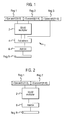
- Figure 1 is a schematic diagram illustrating a method of implementing a multiply-accumulate (MAC) instruction with three source operands.
- Each 32 bit source operand, Operand 1, Operand 2 and Operand 3 is held in a respective register, Reg 1, Reg 2, Reg 3.
- the first and second operands are supplied to a 32 x 32 bit multiplier 2, the outputs of which (in the form of 64 pairs of sum/carry terms) are supplied to a set of full adders in block 4 for the purposes of accumulation.
- the third operand, Operand 3 is also supplied to the full adder block 4.
- the full adder block adds in the third operand the multiplication result.
- the outputs from the full adder block 4 are supplied to an add 64 block 6 which combines the terms from the full adder block and generates a final result.
- the final result is placed in a result register Reg R.
- two of the three operands are multiplied together, and the third operand is added to the result of the multiplication. All three source operands are held in registers (generally implemented as flip-flops), and the final result is stored in a register (flip-flops). Three operands are required, they are all read from a register file at once, and the result is written back to the register file. This enlarges the register file and makes the wiring worse.
- the cost of providing the third register Reg 3 for the third operand, with the corresponding flip-flop and wiring renders a unit such as that illustrated in Figure 1 for implementing a MAC instruction unduly expensive. Moreover, when used for a multiply (MUL) operation, the third register is redundant.
- Figure 2 illustrates a multiply unit which is readily available in many processor cores.
- the multiply unit comprises first and second registers for holding respective operands, a 32 x 32 multiplier block 2, an add 64 block 6 and a result register Reg R.
- Like numerals denote like parts as in Figure 1. Operation of such a multiply unit is known in the art.
- an arithmetic unit for selectively implementing one of a multiply and multiply-accumulate instruction, comprising: a multiplier arranged to receive first and second operands and operable to generate multiplication terms; addition circuitry for receiving multiplication terms from the multiplier and operable to combine them to generate a multiplication result; an output register for receiving the multiplication result from the adder; and accumulator circuitry connected to receive a value stored in the result register and an accumulate control signal which determines whether the arithmetic unit implements a multiply or a multiply-accumulate instruction.
- a further aspect of the invention provides a processor including such a arithmetic unit and an execution unit arranged to execute a first instruction to retrieve an accumulator result from the result register and a second instruction to load an accumulator value into the arithmetic unit.
- Another aspect of the invention provides a method of operating an arithmetic unit for selectively implementing one of a multiply and multiply-accumulate instruction, the method comprising: supplying first and second operands to a multiplier operable to generate multiplication terms; supplying the multiplication terms to addition circuitry operable to generate a multiplication result; storing the multiplication result in a result register of the arithmetic unit; supplying a value stored in the result register to accumulator circuitry; and selectively operating an accumulate control signal supplied to the accumulator circuitry to determine whether the arithmetic unit implements a multiply or a multiply-accumulate instruction.
- a further aspect of the invention provides a method of implementing a multiply instruction in a processor, the method comprising: executing a first instruction to retrieve an accumulator result from a result register of an arithmetic unit in the processor; executing a multiply instruction which causes first and second operands to be supplied to the arithmetic unit which is operable to generate a multiplication result; transferring the multiplication result from the result register to a destination register of the processor; and executing a further instruction to load an accumulator value into the arithmetic unit in readiness for a subsequent multiply-accumulate instruction.
- Figure 3 illustrates a multiply-accumulate unit 1 in accordance with one embodiment of the invention.
- Like numerals denote like parts as in Figures 1 and 2.
- first and second 32 bit operands, Operand 1, Operand 2 are loaded into respective first and second registers Reg 1, Reg 2 by execution of a MAC or MUL instruction.
- the outputs of these registers are connected to a 32 x 32 multiplier block 2 which supplies its outputs (in the form of 64 pairs of sum/carry terms) to a full adder block 4.
- the full adder block receives an additional 64 bit input 3 from a set of logic gates, herein labelled as 8, which allow an accumulator function to be implemented as described in the following. They are referred to herein as accumulator gates.
- the outputs from the full adder block 4 are supplied to an add 64 block 6.
- the register R1 has a clock input 9 for receiving a first clock signal CLK1.
- the result register Reg R2 has a clock input 10 for receiving a second clock signal CLK2, and an output 12 which supplies one input 80 of the accumulator gates.
- the other input of the accumulator gates 8 receives an accumulate signal 82, which is active when a MAC instruction is executed and inactive when a MUL instruction is executed.
- the accumulator gates 8 are shown in more detail in Figure 4.
- a plurality of AND gates (64 in this case) 8 0 ... 8 63 each receive one bit of the result 12 to be accumulated at one input and the accumulate signal 14 at the other input.
- the 64 bit output 16 from the accumulator gates is supplied to the full adder block, which thus acts to accumulate the multiplication results.
- a local accumulator function represents an improvement over the design of Figure 1. It has the effect that the result of previous multiply or multiply-accumulate instructions can be added into future multiply-accumulate instructions, providing the required accumulation.
- the clock CLK1 at input 9 is active.
- the clocks CLK1 and CLK2 are both active and the accumulate signal 14 is set to one. This has the effect that the output of the second result register Reg R2 is supplied to the accumulator 8.
- the clock CLK2 at input 10 is inactive, and the accumulate signal 14 is set to zero. The unit then operates as a normal MUL unit.
- the second result register Reg R2 can be implemented by a bank of flip-flops and holds the accumulation result.
- the accumulation result is selectively fed back into the next operation depending upon whether it is a normal multiplication or a multiply-accumulate instruction. This allows the hardware to be shared between multiply and multiply-accumulate instructions. It will be appreciated that when the MUL/MAC unit is read, it is the result stored in the first result register REG 1 which is read out.
- This design represents an improvement over the design of Figure 1, because it removes the third register for holding a third source operand. However, it still requires an additional 64 flip-flops to implement the second result register Reg R2, and it also requires a row of full adders in the full adder block 4 to perform the accumulation, which is in addition to a normal multiplier design.
- Figure 5 represents a second embodiment of the invention in which the design has been further improved.
- the second result register Reg R2 has been removed, thus saving area.
- a clock signal CLK is supplied to the existing result register Reg R1 at input 16 for clocking the result register in the event of an active instruction, MUL or MAC.
- the output of the result register Reg R1 is supplied to the input of the accumulator gates 8.
- the accumulator gates are as illustrated in Figure 4.
- an accumulator value can be set in the result register Reg R prior to a MAC operation by executing the instruction:
- the multiply-accumulate unit can switch between operating as a multiplier and a multiply-accumulate unit.
- the multiply-accumulate unit result needs to be removed so that the unit can operate as a multiplier
- the first of the above-referenced instructions is implemented.
- the initial accumulator value can be set using the second of the above-referenced instructions.
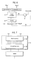
- This multiplier block 2 includes a booth recoding block 20 which receives the two operands Op 1, Op 2 and which provides an output of seventeen terms. The seventeen terms are fed to a carry-save addition block 22 which implements carry-save addition of the seventeen terms down to two terms. That is, for each bit position of the result (63 to 0) a maximum of 17 bits needs to be added.
- a Wallace tree construction for adding 17 terms is well known in the art. It comprises 64 columns of varying heights, the heights being determined by the number of levels in a column.
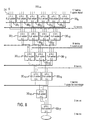
- Figure 8 illustrates one column COL m of a Wallace tree which will add 17 terms.
- the first level of the Wallace tree comprises six 3 bit adders 30 1 ... 30 6 each having three inputs labelled a, b, c, a sum output s and a carry output c. As there are seventeen terms, the first input of the first full adder 30 1 (labelled 24) is spare.
- the first level of the Wallace tree provides its carry outputs to the adjacent column of the Wallace tree (not shown), while its sum outputs are supplied to respective adders 30 7 ... 30 10 in the second level of this column of the Wallace tree.
- the sum outputs from the first two adders 30 1 , 30 2 in the first level are supplied to the first adder 30 7 in the second level
- the sum outputs from the second two adders 30 3 , 30 4 in the first level are supplied to the second adder 30 3 in the second level
- the sum output from the fifth adder 30 5 in the first level is supplied to the third adder 30 9 in the second level
- the sum output from the sixth adder 30 6 in the first level is supplied to the fourth adder 30 10 in the second level.
- the adders in the second level receive carry inputs from the adjacent column of the Wallace tree on the other side (not shown).
- the four 3 bit adders of the second level 30 7 ... 30 10 receive a total of twelve terms.
- the third level of the Wallace tree comprises three 3 bit adders 30 11 ... 30 13 , which are set to receive eight terms, being four sum terms from the preceding level of the Wallace tree and four carry terms from the adjacent column. This means that there is another spare input, labelled 26, in the third level of the Wallace tree.
- the fourth level of the Wallace tree comprises two 3 bit adders 30 14 , 30 15 which receive six terms, being two sum terms from the preceding level of the Wallace tree and three carry terms from the adjacent column.
- the fourth level of the Wallace tree outputs two carry terms to the next column and two sum terms to the next level of the Wallace tree which comprises a 3 bit adder 30 16 .
- Two carry terms are received from the adjacent column, one of which is supplied to the 3 bit adder constituting the fifth level of the Wallace tree, and the other of which is supplied to a final stage adder 30 17 .
- each column of the Wallace tree has two spare inputs, one, 24, in the first level and one, 26, in the third level.
- Each output from the accumulator 8 can be applied to one of these spare inputs.
- Either the spare inputs in the first level or the spare inputs in the third level can be used, though it would seem advantageous to use the spare inputs in the third level.
- the signal of same bit weight from the accumulator is applied to the column of the Wallace tree having the same bit weight.
- Figure 9 shows this schematically.
- the first and second instructions for removing the accumulated value and resetting the accumulated value as described above in relation to the embodiment of Figure 5 are also applicable to the embodiment of Figure 6.
- FIG 10 is a schematic diagram of a processor which uses a multiply-accumulate unit 1 as hereinabove described.
- the processor comprises an instruction memory 100 for holding instructions including multiply instructions, multiply-accumulate instructions and special instructions of the type described above.
- a fetch decode block 102 fetches instructions from the instruction memory 100 and supplies them to an execution stage 104 for execution.
- the execution stage includes or is associated with the multiply-accumulate unit 1 and cooperates with a register file 106 which includes source and destination registers for cooperation with the multiply-accumulate unit 1 as hereinabove described.
Landscapes
- Engineering & Computer Science (AREA)
- Physics & Mathematics (AREA)
- General Physics & Mathematics (AREA)
- Theoretical Computer Science (AREA)
- Computational Mathematics (AREA)
- Computing Systems (AREA)
- Mathematical Analysis (AREA)
- Mathematical Optimization (AREA)
- Pure & Applied Mathematics (AREA)
- General Engineering & Computer Science (AREA)
- Complex Calculations (AREA)
Abstract
Description
- The present invention relates to a multiply-accumulate unit for selectively implementing multiply and multiply-accumulate operations.
- Multiply-accumulate (MAC) operations are required in processor cores. Multiply-accumulate is an important and expensive operation. It is frequently used in digital signal processing and video/graphics applications. As a result, any improvement in the delay for performing this operation has a significant impact on various aspects of processor performance.
- Figure 1 is a schematic diagram illustrating a method of implementing a multiply-accumulate (MAC) instruction with three source operands. Each 32 bit source operand,
Operand 1,Operand 2 andOperand 3, is held in a respective register,Reg 1,Reg 2,Reg 3. The first and second operands are supplied to a 32 x 32bit multiplier 2, the outputs of which (in the form of 64 pairs of sum/carry terms) are supplied to a set of full adders inblock 4 for the purposes of accumulation. The third operand, Operand 3, is also supplied to thefull adder block 4. The full adder block adds in the third operand the multiplication result. The outputs from thefull adder block 4 are supplied to anadd 64block 6 which combines the terms from the full adder block and generates a final result. The final result is placed in a result register Reg R. According to this schematic, two of the three operands are multiplied together, and the third operand is added to the result of the multiplication. All three source operands are held in registers (generally implemented as flip-flops), and the final result is stored in a register (flip-flops). Three operands are required, they are all read from a register file at once, and the result is written back to the register file. This enlarges the register file and makes the wiring worse. - The cost of providing the
third register Reg 3 for the third operand, with the corresponding flip-flop and wiring renders a unit such as that illustrated in Figure 1 for implementing a MAC instruction unduly expensive. Moreover, when used for a multiply (MUL) operation, the third register is redundant. - Figure 2 illustrates a multiply unit which is readily available in many processor cores. The multiply unit comprises first and second registers for holding respective operands, a 32 x 32
multiplier block 2, an add 64block 6 and a result register Reg R. Like numerals denote like parts as in Figure 1. Operation of such a multiply unit is known in the art. - It is an aim of the present invention to make use of the existing available multiplier (MUL) unit to implement MAC instructions, to obviate the need for an extra input register for holding a third source operand.
- According to an aspect of the present invention there is provided an arithmetic unit for selectively implementing one of a multiply and multiply-accumulate instruction, comprising: a multiplier arranged to receive first and second operands and operable to generate multiplication terms; addition circuitry for receiving multiplication terms from the multiplier and operable to combine them to generate a multiplication result; an output register for receiving the multiplication result from the adder; and accumulator circuitry connected to receive a value stored in the result register and an accumulate control signal which determines whether the arithmetic unit implements a multiply or a multiply-accumulate instruction.
- A further aspect of the invention provides a processor including such a arithmetic unit and an execution unit arranged to execute a first instruction to retrieve an accumulator result from the result register and a second instruction to load an accumulator value into the arithmetic unit.
- Another aspect of the invention provides a method of operating an arithmetic unit for selectively implementing one of a multiply and multiply-accumulate instruction, the method comprising: supplying first and second operands to a multiplier operable to generate multiplication terms; supplying the multiplication terms to addition circuitry operable to generate a multiplication result; storing the multiplication result in a result register of the arithmetic unit; supplying a value stored in the result register to accumulator circuitry; and selectively operating an accumulate control signal supplied to the accumulator circuitry to determine whether the arithmetic unit implements a multiply or a multiply-accumulate instruction.
- A further aspect of the invention provides a method of implementing a multiply instruction in a processor, the method comprising: executing a first instruction to retrieve an accumulator result from a result register of an arithmetic unit in the processor; executing a multiply instruction which causes first and second operands to be supplied to the arithmetic unit which is operable to generate a multiplication result; transferring the multiplication result from the result register to a destination register of the processor; and executing a further instruction to load an accumulator value into the arithmetic unit in readiness for a subsequent multiply-accumulate instruction.
- For a better understanding of the present invention and to show how the same may be carried into effect, reference will now be made by way of example to the accompanying drawings, in which:
- Figure 1 is a schematic block diagram of a unit for implementing a MAC instruction;
- Figure 2 is a schematic block diagram of a unit for implementing a MUL instruction;
- Figure 3 is a schematic block diagram of a MUL/MAC unit in accordance with one embodiment of the invention;
- Figure 4 is a schematic block diagram of accumulating gates;
- Figure 5 is a schematic block diagram of a MUL/MAC unit in accordance with another embodiment of the invention;
- Figure 6 is a schematic block diagram of a MUL/MAC unit in accordance with another embodiment of the invention;
- Figure 7 is a schematic block diagram of a multiplier; and
- Figure 8 is a schematic block diagram of one column of a Wallace tree.
- Figure 3 illustrates a multiply-accumulate
unit 1 in accordance with one embodiment of the invention. Like numerals denote like parts as in Figures 1 and 2. - In the multiply-accumulate unit of Figure 3, first and second 32 bit operands,
Operand 1,Operand 2, are loaded into respective first andsecond registers Reg 1,Reg 2 by execution of a MAC or MUL instruction. The outputs of these registers are connected to a 32 x 32multiplier block 2 which supplies its outputs (in the form of 64 pairs of sum/carry terms) to afull adder block 4. In this case, the full adder block receives an additional 64bit input 3 from a set of logic gates, herein labelled as 8, which allow an accumulator function to be implemented as described in the following. They are referred to herein as accumulator gates. The outputs from thefull adder block 4 are supplied to an add 64block 6. In this case, there are two result registers, Reg R1 and Reg R2. The register R1 has a clock input 9 for receiving a first clock signal CLK1. The result register Reg R2 has aclock input 10 for receiving a second clock signal CLK2, and anoutput 12 which supplies oneinput 80 of the accumulator gates. The other input of theaccumulator gates 8 receives an accumulatesignal 82, which is active when a MAC instruction is executed and inactive when a MUL instruction is executed. - The
accumulator gates 8 are shown in more detail in Figure 4. A plurality of AND gates (64 in this case) 80 ... 863, each receive one bit of theresult 12 to be accumulated at one input and the accumulate signal 14 at the other input. The 64bit output 16 from the accumulator gates is supplied to the full adder block, which thus acts to accumulate the multiplication results. - The provision of a local accumulator function represents an improvement over the design of Figure 1. It has the effect that the result of previous multiply or multiply-accumulate instructions can be added into future multiply-accumulate instructions, providing the required accumulation. If a MUL operation is to be implemented, the clock CLK1 at input 9 is active. If a MAC operation is to be implemented, the clocks CLK1 and CLK2 are both active and the accumulate signal 14 is set to one. This has the effect that the output of the second result register Reg R2 is supplied to the
accumulator 8. If a MAC operation is not needed, the clock CLK2 atinput 10 is inactive, and the accumulate signal 14 is set to zero. The unit then operates as a normal MUL unit. - The second result register Reg R2 can be implemented by a bank of flip-flops and holds the accumulation result. The accumulation result is selectively fed back into the next operation depending upon whether it is a normal multiplication or a multiply-accumulate instruction. This allows the hardware to be shared between multiply and multiply-accumulate instructions. It will be appreciated that when the MUL/MAC unit is read, it is the result stored in the first
result register REG 1 which is read out. - This design represents an improvement over the design of Figure 1, because it removes the third register for holding a third source operand. However, it still requires an additional 64 flip-flops to implement the second result register Reg R2, and it also requires a row of full adders in the
full adder block 4 to perform the accumulation, which is in addition to a normal multiplier design. - Figure 5 represents a second embodiment of the invention in which the design has been further improved. In the embodiment of Figure 4, the second result register Reg R2 has been removed, thus saving area. Moreover, because 64 less flip-flops are being clocked for a MAC operation, power is saved. A clock signal CLK is supplied to the existing result register Reg R1 at
input 16 for clocking the result register in the event of an active instruction, MUL or MAC. The output of the result register Reg R1 is supplied to the input of theaccumulator gates 8. The accumulator gates are as illustrated in Figure 4. - The removal of the second result register in the embodiment of Figure 5 means that software executed on a CPU to implement multiplication and multiply-accumulate operations needs to be slightly modified to take this into account. It will readily be appreciated that when the
clock signal 16 is active, with the accumulate signal 14 set to zero, the multiplication result will remain "refreshed" in the result register Reg R. However, when the accumulate signal is set, at the first active clock pulse the previous multiplication result will be overwritten with the accumulated result. Thus this accumulated result needs to be read out at the end of the MAC operation by executing an instruction as follows: - MAC r0, r0, rx
- Conversely, an accumulator value can be set in the result register Reg R prior to a MAC operation by executing the instruction:
- MUL<accumulator value to set>, 1,
- Using these two instructions means that the multiply-accumulate unit can switch between operating as a multiplier and a multiply-accumulate unit. When the multiply-accumulate unit result needs to be removed so that the unit can operate as a multiplier, the first of the above-referenced instructions is implemented. When the unit ceases to be used as a multiplier and needs to be used again as a multiply-accumulate unit, the initial accumulator value can be set using the second of the above-referenced instructions.
- The design of Figure 5 is cheaper still to implement than the design of Figure 3, because it avoids the need for the second result register.
- A still further improvement can be made which will now be described with reference to Figures 6 to 8. As shown in Figure 6, it is possible for some multiplier configurations to be implemented without the full adder block leading to the construction of the multiply-accumulate unit shown in Figure 6 where the outputs of the multiplier are fed directly to the add 64 block, and the output of the accumulator is fed directly into the
multiplier block 2. - One example of a multiplier configuration which will allow this optimisation is illustrated in Figure 7. This
multiplier block 2 includes abooth recoding block 20 which receives the twooperands Op 1,Op 2 and which provides an output of seventeen terms. The seventeen terms are fed to a carry-saveaddition block 22 which implements carry-save addition of the seventeen terms down to two terms. That is, for each bit position of the result (63 to 0) a maximum of 17 bits needs to be added. A Wallace tree construction for adding 17 terms is well known in the art. It comprises 64 columns of varying heights, the heights being determined by the number of levels in a column. Figure 8 illustrates one column COLm of a Wallace tree which will add 17 terms. The first level of the Wallace tree comprises six 3 bit adders 301 ... 306 each having three inputs labelled a, b, c, a sum output s and a carry output c. As there are seventeen terms, the first input of the first full adder 301 (labelled 24) is spare. The first level of the Wallace tree provides its carry outputs to the adjacent column of the Wallace tree (not shown), while its sum outputs are supplied to respective adders 307 ... 3010 in the second level of this column of the Wallace tree. That is, the sum outputs from the first two adders 301, 302 in the first level are supplied to the first adder 307 in the second level, the sum outputs from the second two adders 303, 304 in the first level are supplied to the second adder 303 in the second level, the sum output from the fifth adder 305 in the first level is supplied to the third adder 309 in the second level and the sum output from the sixth adder 306 in the first level is supplied to the fourth adder 3010 in the second level. In addition, the adders in the second level receive carry inputs from the adjacent column of the Wallace tree on the other side (not shown). The four 3 bit adders of the second level 307 ... 3010 receive a total of twelve terms. The third level of the Wallace tree comprises three 3 bit adders 3011 ... 3013, which are set to receive eight terms, being four sum terms from the preceding level of the Wallace tree and four carry terms from the adjacent column. This means that there is another spare input, labelled 26, in the third level of the Wallace tree. - The fourth level of the Wallace tree comprises two 3 bit adders 3014, 3015 which receive six terms, being two sum terms from the preceding level of the Wallace tree and three carry terms from the adjacent column. The fourth level of the Wallace tree outputs two carry terms to the next column and two sum terms to the next level of the Wallace tree which comprises a 3 bit adder 3016. Two carry terms are received from the adjacent column, one of which is supplied to the 3 bit adder constituting the fifth level of the Wallace tree, and the other of which is supplied to a final stage adder 3017.
- It can be seen from the above that each column of the Wallace tree has two spare inputs, one, 24, in the first level and one, 26, in the third level. Each output from the
accumulator 8 can be applied to one of these spare inputs. Either the spare inputs in the first level or the spare inputs in the third level can be used, though it would seem advantageous to use the spare inputs in the third level. It will be appreciated that the signal of same bit weight from the accumulator is applied to the column of the Wallace tree having the same bit weight. Figure 9 shows this schematically. - By introducing the value to the accumulator directly into the Wallace tree construction, no full adders are needed to achieve the multiply-accumulate operation.
- The first and second instructions for removing the accumulated value and resetting the accumulated value as described above in relation to the embodiment of Figure 5 are also applicable to the embodiment of Figure 6.
- The above-described embodiments of Figures 5 and 6 provide an arithmetic unit which can perform a multiply or multiply-accumulate operate using a shared result register, therefore not adding any extra state (for example flip-flops). Moreover, all of the above-described embodiments provide an arithmetic unit in which a multiply-accumulate operation can be carried out with the same logical delay as a multiply operation.
- Figure 10 is a schematic diagram of a processor which uses a multiply-accumulate
unit 1 as hereinabove described. The processor comprises aninstruction memory 100 for holding instructions including multiply instructions, multiply-accumulate instructions and special instructions of the type described above. A fetchdecode block 102 fetches instructions from theinstruction memory 100 and supplies them to anexecution stage 104 for execution. The execution stage includes or is associated with the multiply-accumulateunit 1 and cooperates with aregister file 106 which includes source and destination registers for cooperation with the multiply-accumulateunit 1 as hereinabove described.
Claims (12)
- An arithmetic unit for selectively implementing one of a multiply and multiply-accumulate instruction, comprising:a multiplier (2) arranged to receive first and second operands and operable to generate multiplication terms;addition circuitry (6) for receiving multiplication terms from the multiplier and operable to combine them to generate a multiplication result;a result register (Reg R) for receiving the multiplication result from the adder; andaccumulator circuitry (8) connected to receive a value stored in the result register and an accumulate control signal which determines whether the arithmetic unit implements a multiply or a multiply-accumulate instruction.
- An arithmetic unit according to claim 1, wherein the addition circuitry comprises a set of full adders (4) connected to receive the multiplication terms from the multiplier, wherein an output (3) from the accumulator circuitry (8) is connected to the set of full adders.
- An arithmetic unit according to claim 1 or 2, wherein the result register is operable under the control of a clock signal (CLK2; CLK).
- An arithmetic unit according to claim 3, which comprises an additional result register (Reg R1) for receiving the multiplication result operable under the control of an additional clock signal (CLK1), wherein the clock signal (CLK2) for the first result register (Reg R2) is active only if the arithmetic unit is implementing a MAC instruction.
- An arithmetic unit according to any preceding claim, wherein the accumulator circuitry comprises a plurality of AND gates (80 ... 863), each providing an output of certain bit weight.
- An arithmetic unit according to claim 1, wherein the multiplier comprises a Wallace tree having a plurality of columns, each column having a plurality of adders (30), and wherein each output of the accumulator is connected to at least one adder in each respective column of the Wallace tree construction, in dependence on their bit weight.
- An arithmetic unit according to claim 6, wherein the multiplier comprises a Booth recoding block (20).
- An arithmetic unit according to any preceding claim which comprises first and second input registers for receiving respectively said first and second operands.
- A processor for implementing multiply-accumulate and multiply instructions, the processor comprising an arithmetic unit (1) according to any preceding, and an execution unit (104) arranged to execute a first instruction to retrieve an accumulator result from the result register and a second instruction to load an accumulator value into the arithmetic unit.
- A method of operating an arithmetic unit for selectively implementing one of a multiply and multiply-accumulate instruction, the method comprising:supplying first and second operands to a multiplier operable to generate multiplication terms;supplying the multiplication terms to addition circuitry operable to generate a multiplication result;storing the multiplication result in a result register of the arithmetic unit;supplying a value stored in the result register to accumulator circuitry; and selectively operating an accumulate control signal supplied to the accumulator circuitry to determine whether the arithmetic unit implements a multiply or a multiply-accumulate instruction.
- A method according to claim 10, which comprises controlling the result register using a clock signal.
- A method of implementing a multiply instruction in a processor, the method comprising:executing a first instruction to retrieve an accumulator result from a result register of an arithmetic unit in the processor;executing a multiply instruction which causes first and second operands to be supplied to the arithmetic unit which is operable to generate a multiplication result;transferring the multiplication result from the result register to a destination register of the processor; andexecuting a further instruction to load an accumulator value into the arithmetic unit in readiness for a subsequent multiply-accumulate instruction.
Priority Applications (2)
| Application Number | Priority Date | Filing Date | Title |
|---|---|---|---|
| EP05252194A EP1710691A1 (en) | 2005-04-07 | 2005-04-07 | MAC/MUL unit |
| US11/400,020 US7730118B2 (en) | 2005-04-07 | 2006-04-07 | Multiply-accumulate unit and method of operation |
Applications Claiming Priority (1)
| Application Number | Priority Date | Filing Date | Title |
|---|---|---|---|
| EP05252194A EP1710691A1 (en) | 2005-04-07 | 2005-04-07 | MAC/MUL unit |
Publications (1)
| Publication Number | Publication Date |
|---|---|
| EP1710691A1 true EP1710691A1 (en) | 2006-10-11 |
Family
ID=34940742
Family Applications (1)
| Application Number | Title | Priority Date | Filing Date |
|---|---|---|---|
| EP05252194A Withdrawn EP1710691A1 (en) | 2005-04-07 | 2005-04-07 | MAC/MUL unit |
Country Status (2)
| Country | Link |
|---|---|
| US (1) | US7730118B2 (en) |
| EP (1) | EP1710691A1 (en) |
Cited By (2)
| Publication number | Priority date | Publication date | Assignee | Title |
|---|---|---|---|---|
| GB2474901A (en) * | 2009-10-30 | 2011-05-04 | Advanced Risc Mach Ltd | Multiply-accumulate instruction which adds or subtracts based on a predicate value |
| CN103984520A (en) * | 2014-04-22 | 2014-08-13 | 浙江大学 | Self-adjusting multiply accumulation device for lossless audio decoding algorithm |
Families Citing this family (7)
| Publication number | Priority date | Publication date | Assignee | Title |
|---|---|---|---|---|
| US9563401B2 (en) | 2012-12-07 | 2017-02-07 | Wave Computing, Inc. | Extensible iterative multiplier |
| US10289382B2 (en) | 2012-12-20 | 2019-05-14 | Wave Computing, Inc. | Selectively combinable directional shifters |
| US9933996B2 (en) | 2012-12-20 | 2018-04-03 | Wave Computing, Inc. | Selectively combinable shifters |
| US11334319B2 (en) | 2017-06-30 | 2022-05-17 | Intel Corporation | Apparatus and method for multiplication and accumulation of complex values |
| WO2019005132A1 (en) | 2017-06-30 | 2019-01-03 | Intel Corporation | APPARATUS AND METHOD FOR MULTIPLICATION AND CUMULATION OF COMPLEX VALUES |
| US10872295B1 (en) | 2019-09-19 | 2020-12-22 | Hong Kong Applied Science and Technology Institute Company, Limited | Residual quantization of bit-shift weights in an artificial neural network |
| WO2025183589A1 (en) * | 2024-02-27 | 2025-09-04 | Общество С Ограниченной Ответственностью "Мотив Нейроморфные Технологии" | Pipelined multiplier |
Citations (3)
| Publication number | Priority date | Publication date | Assignee | Title |
|---|---|---|---|---|
| US5436860A (en) * | 1994-05-26 | 1995-07-25 | Motorola, Inc. | Combined multiplier/shifter and method therefor |
| US5847981A (en) * | 1997-09-04 | 1998-12-08 | Motorola, Inc. | Multiply and accumulate circuit |
| US20030172101A1 (en) * | 1999-12-23 | 2003-09-11 | Yuyun Liao | Processing multiply-accumulate operations in a single cycle |
Family Cites Families (2)
| Publication number | Priority date | Publication date | Assignee | Title |
|---|---|---|---|---|
| JPS6347874A (en) * | 1986-08-16 | 1988-02-29 | Nec Corp | Arithmetic unit |
| US7107305B2 (en) * | 2001-10-05 | 2006-09-12 | Intel Corporation | Multiply-accumulate (MAC) unit for single-instruction/multiple-data (SIMD) instructions |
-
2005
- 2005-04-07 EP EP05252194A patent/EP1710691A1/en not_active Withdrawn
-
2006
- 2006-04-07 US US11/400,020 patent/US7730118B2/en active Active
Patent Citations (3)
| Publication number | Priority date | Publication date | Assignee | Title |
|---|---|---|---|---|
| US5436860A (en) * | 1994-05-26 | 1995-07-25 | Motorola, Inc. | Combined multiplier/shifter and method therefor |
| US5847981A (en) * | 1997-09-04 | 1998-12-08 | Motorola, Inc. | Multiply and accumulate circuit |
| US20030172101A1 (en) * | 1999-12-23 | 2003-09-11 | Yuyun Liao | Processing multiply-accumulate operations in a single cycle |
Non-Patent Citations (1)
| Title |
|---|
| LIAO Y ET AL: "A HIGH-PERFORMANCE AND LOW-POWER 32-BIT MULTIPLY-ACCUMULATE UNIT WITH SINGLE-INSTRUCTION-MULTIPLE-DATA (SIMD) FEATURE", IEEE JOURNAL OF SOLID-STATE CIRCUITS, IEEE INC. NEW YORK, US, vol. 37, no. 7, July 2002 (2002-07-01), pages 926 - 931, XP001221317, ISSN: 0018-9200 * |
Cited By (6)
| Publication number | Priority date | Publication date | Assignee | Title |
|---|---|---|---|---|
| GB2474901A (en) * | 2009-10-30 | 2011-05-04 | Advanced Risc Mach Ltd | Multiply-accumulate instruction which adds or subtracts based on a predicate value |
| CN102053817A (en) * | 2009-10-30 | 2011-05-11 | Arm有限公司 | Multiply-accumulate instruction which adds or subtracts based on a predicate value |
| US8595280B2 (en) | 2009-10-30 | 2013-11-26 | Arm Limited | Apparatus and method for performing multiply-accumulate operations |
| GB2474901B (en) * | 2009-10-30 | 2015-01-07 | Advanced Risc Mach Ltd | Apparatus and method for performing multiply-accumulate operations |
| CN102053817B (en) * | 2009-10-30 | 2015-09-09 | Arm有限公司 | For performing equipment and the method for multiplication accumulating operation |
| CN103984520A (en) * | 2014-04-22 | 2014-08-13 | 浙江大学 | Self-adjusting multiply accumulation device for lossless audio decoding algorithm |
Also Published As
| Publication number | Publication date |
|---|---|
| US7730118B2 (en) | 2010-06-01 |
| US20060277245A1 (en) | 2006-12-07 |
Similar Documents
| Publication | Publication Date | Title |
|---|---|---|
| US11188330B2 (en) | Vector multiply-add instruction | |
| US7124160B2 (en) | Processing architecture having parallel arithmetic capability | |
| EP2521968B1 (en) | Hardware for performing arithmetic operations | |
| JP3555140B2 (en) | Semiconductor floorplan and method for register rename circuit | |
| EP2435906B1 (en) | Dsp engine with implicit mixed operands | |
| US6061780A (en) | Execution unit chaining for single cycle extract instruction having one serial shift left and one serial shift right execution units | |
| EP0754998A1 (en) | An arithmetic unit | |
| US20040267855A1 (en) | Method and apparatus for implementing processor instructions for accelerating public-key cryptography | |
| JPH10187438A (en) | How to reduce transitions for multiplier inputs. | |
| US7013321B2 (en) | Methods and apparatus for performing parallel integer multiply accumulate operations | |
| JP3683773B2 (en) | Floating point unit that uses a standard MAC unit to perform SIMD operations | |
| US9372665B2 (en) | Method and apparatus for multiplying binary operands | |
| WO2010011240A1 (en) | Circular register array of a computer | |
| US20070239970A1 (en) | Apparatus For Cooperative Sharing Of Operand Access Port Of A Banked Register File | |
| US5301139A (en) | Shifter circuit for multiple precision division | |
| US7730118B2 (en) | Multiply-accumulate unit and method of operation | |
| US20110314265A1 (en) | Processors operable to allow flexible instruction alignment | |
| US20040143613A1 (en) | Floating point bypass register to resolve data dependencies in pipelined instruction sequences | |
| US7234044B1 (en) | Processor registers having state information | |
| TWI807927B (en) | Vector processor with vector reduction method and element reduction method | |
| KR100481586B1 (en) | Apparatus for modular multiplication | |
| JP2008242947A (en) | Semiconductor device | |
| JP2875864B2 (en) | Pipeline processing method | |
| CN101042641B (en) | Digital signal processor with dynamic submitting pipeline function | |
| US6792442B1 (en) | Signal processor and product-sum operating device for use therein with rounding function |
Legal Events
| Date | Code | Title | Description |
|---|---|---|---|
| PUAI | Public reference made under article 153(3) epc to a published international application that has entered the european phase |
Free format text: ORIGINAL CODE: 0009012 |
|
| AK | Designated contracting states |
Kind code of ref document: A1 Designated state(s): AT BE BG CH CY CZ DE DK EE ES FI FR GB GR HU IE IS IT LI LT LU MC NL PL PT RO SE SI SK TR |
|
| AX | Request for extension of the european patent |
Extension state: AL BA HR LV MK YU |
|
| 17P | Request for examination filed |
Effective date: 20070329 |
|
| AKX | Designation fees paid |
Designated state(s): DE FR GB IT |
|
| 17Q | First examination report despatched |
Effective date: 20080207 |
|
| STAA | Information on the status of an ep patent application or granted ep patent |
Free format text: STATUS: THE APPLICATION IS DEEMED TO BE WITHDRAWN |
|
| 18D | Application deemed to be withdrawn |
Effective date: 20080819 |