EP1710661A1 - Monitoring circuit - Google Patents
Monitoring circuit Download PDFInfo
- Publication number
- EP1710661A1 EP1710661A1 EP04807840A EP04807840A EP1710661A1 EP 1710661 A1 EP1710661 A1 EP 1710661A1 EP 04807840 A EP04807840 A EP 04807840A EP 04807840 A EP04807840 A EP 04807840A EP 1710661 A1 EP1710661 A1 EP 1710661A1
- Authority
- EP
- European Patent Office
- Prior art keywords
- voltage
- capacitor
- microcomputer
- monitoring
- monitoring circuit
- Prior art date
- Legal status (The legal status is an assumption and is not a legal conclusion. Google has not performed a legal analysis and makes no representation as to the accuracy of the status listed.)
- Withdrawn
Links
Images


Classifications
-
- G—PHYSICS
- G11—INFORMATION STORAGE
- G11C—STATIC STORES
- G11C5/00—Details of stores covered by group G11C11/00
- G11C5/14—Power supply arrangements, e.g. power down, chip selection or deselection, layout of wirings or power grids, or multiple supply levels
-
- G—PHYSICS
- G06—COMPUTING OR CALCULATING; COUNTING
- G06F—ELECTRIC DIGITAL DATA PROCESSING
- G06F1/00—Details not covered by groups G06F3/00 - G06F13/00 and G06F21/00
- G06F1/26—Power supply means, e.g. regulation thereof
- G06F1/28—Supervision thereof, e.g. detecting power-supply failure by out of limits supervision
-
- G—PHYSICS
- G06—COMPUTING OR CALCULATING; COUNTING
- G06F—ELECTRIC DIGITAL DATA PROCESSING
- G06F1/00—Details not covered by groups G06F3/00 - G06F13/00 and G06F21/00
- G06F1/24—Resetting means
-
- G—PHYSICS
- G06—COMPUTING OR CALCULATING; COUNTING
- G06F—ELECTRIC DIGITAL DATA PROCESSING
- G06F1/00—Details not covered by groups G06F3/00 - G06F13/00 and G06F21/00
- G06F1/26—Power supply means, e.g. regulation thereof
- G06F1/30—Means for acting in the event of power-supply failure or interruption, e.g. power-supply fluctuations
-
- G—PHYSICS
- G11—INFORMATION STORAGE
- G11C—STATIC STORES
- G11C29/00—Checking stores for correct operation ; Subsequent repair; Testing stores during standby or offline operation
Definitions
- the present invention relates to a monitoring circuit to be an effective technique utilizing a fail-safe system for detecting an abnormal operation of a microcomputer to automatically take avoiding measures.
- the monitoring circuit can detect that the microcomputer is not normally operated by only monitoring the normal operation clock from the microcomputer for a certain time. For this reason, when a power to be supplied to the microcomputer is decreased, it is impossible to safely reset the microcomputer immediately. Even if the microcomputer recovers the operation when a power supply is returned from a power decreasing state to a stable state, therefore, there is a possibility that the microcomputer might malfunction due to a memory or a register which is provided in the microcomputer which interrupts an operation by a decrease in a power.
- the invention has been made to solve the problems of the conventional art and has an object to provide a semiconductor device comprising a monitoring circuit capable of safely resetting a microcomputer in a decrease in a power, a monitoring circuit capable of setting a reset release section to be constant and the monitoring circuit, and furthermore, an electronic apparatus mounting the semiconductor device thereon.
- a first aspect of the invention is directed to a monitoring circuit comprising a capacitor, charging means for charging the capacitor, discharging means for discharging the capacitor, voltage comparing means for comparing a certain reference voltage with a charging voltage of the capacitor, thereby generating a signal for resetting an operation of a monitoring object when the capacitor is charged to have a certain voltage or more, and source voltage deciding means for monitoring a source voltage of the monitoring object and resetting the operation of the monitoring object when the source voltage of the monitoring object is equal to or lower than a certain voltage.
- a second aspect of the invention is directed to a monitoring circuit comprising a capacitor, charging means for charging the capacitor, first discharging means for discharging the capacitor, second discharging means for discharging the capacitor, voltage comparing means for comparing a certain reference voltage with a voltage of the capacitor, thereby generating a signal for resetting an operation of a monitoring object when the capacitor is charged to have a certain voltage or more, and source voltage deciding means for monitoring a source voltage of the monitoring object and resetting the operation of the monitoring object when the source voltage of the monitoring object is equal to or lower than a certain voltage.
- a third aspect of the invention is directed to the monitoring circuit according to the first or second aspect of the invention, wherein the source voltage deciding means is constituted by a comparator and the charging means is constituted by a current source.
- a fourth aspect of the invention is directed to the monitoring circuit according to the second or third aspect of the invention, wherein the first discharging means is constituted by a current source and the second discharging means is constituted by an analog switch, and either or both of the first and second discharging means is/are operated to invert an output of the voltage comparing means, thereby resetting the monitoring object when the source voltage of the monitoring object is equal to or lower than a certain voltage.
- a fifth aspect of the invention is directed to the monitoring circuit according to the second or third aspect of the invention, wherein the first discharging means is constituted by a current source and the second discharging means is constituted by an N-type MOS transistor.
- a sixth aspect of the invention is directed to the monitoring circuit according to any of the first to fifth aspects of the invention, wherein the voltage comparing means is constituted by a window comparator.
- a seventh aspect of the invention is directed to the monitoring circuit according to any of the first to fifth aspects of the invention, wherein the voltage comparingmeansisconstituted byahysteresiscomparator.
- An eighth aspect of the invention is directed to a semiconductor device comprising the monitoring circuit according to any of the first to seventh aspects of the invention.
- a ninth aspect of the invention is directed to a semiconductor device comprising the monitoring circuit according to any of the first to seventh aspects of the invention in which the capacitor is provided on an outside of the semiconductor device.
- a tenth aspect of the invention is directed to an electronic apparatus comprising the semiconductor device according to the eighth or ninth aspect of the invention and a microcomputer to be monitored by the semiconductor device.
- the microcomputer can be reset safely also in a decrease in a power, a section for the reset release state of the microcomputer can be maintained to have a certain length and a reset signal can be generated in a desirable timing. Therefore, it is possible to eliminate a time loss caused before resetting the microcomputer. Furthermore, the control of the electronic apparatus comprising the microcomputer can be set to be more accurate.
- 1 denotes a charging circuit
- 2a denotes a constant current source
- 2b denotes an N-type MOS transistor
- 3 denotes a capacitor
- 4 denotes a window comparator
- 5 denotes a comparator
- 6 and 9 denote a logic circuit
- 7 denotes a microcomputer
- 8a and 8b denote a source voltage
- 10a, 10b and 10c denote a resistor
- 16 denotes a monitoring circuit.
- Fig. 1 shows a monitoring circuit 15 according to a structure of the invention.
- a current source 1 to be a charging circuit and a current source 2a to be a discharging circuit are connected to a capacitor 3, and the capacitor 3 is connected to an input terminal of a window comparator 4.
- a threshold of the window comparator 4 an electric potential applied from a source voltage 8a is divided by resistors 10a, 10b and 10c and the voltages thus divided are set to be reference voltages.
- a logic circuit 6 is operated in order to/not to transmit a reset output of the window comparator 4 to a microcomputer 7.
- a source voltage of the microcomputer 7 is also monitored in a comparator 5, and at the same time, a reset signal is output from the comparator 5 to the microcomputer 7 in a decrease in an electricity of the microcomputer 7 and a trigger signal for discharging an electric charge of the capacitor 3 is transmitted to a logic circuit 9.
- FIG. 2 An operation of a monitoring circuit 15 will be described with reference to Fig. 2.
- an axis of ordinate indicates a voltage and an axis of abscissa indicates a time.
- (a) indicates a source voltage 8b
- (b) indicates a normal operation clock sent from the microcomputer 7
- (c) indicates a reset signal sent from the comparator 5 and the window comparator 4 to the microcomputer 7 (reset with LOW)
- (d) indicates an amount of electric charges of the capacitor 3 which is measured by the window comparator 4
- (e) indicates an output of the window comparator 4.
- a vertical line (1) in Fig. 2 indicates a timing in which the monitoring circuit 15 and the microcomputer 7 according to the invention shown in Fig. 1 are turned on.
- a vertical line (2) in Fig. 2 indicates a timing in which the source voltage 8b is higher than a threshold voltage (VDDthh) on the HIGH side of the comparator 5 so that the charging circuit 1 is activated to start to store electric charges in the capacitor 3. At this time, moreover, the microcomputer 7 is brought into a reset release state.
- VDDthh threshold voltage
- a vertical line (3) in Fig. 2 indicates a timing of an input of a normal operation clock from the microcomputer 7 which is to be input to the logic circuit 9 of the monitoring circuit 15 when the microcomputer 7 is operated normally.
- the charging circuit 1 is stopped so that the discharging circuit 2a is activated. Therefore, the electric charges of the capacitor 3 are discharged.
- a vertical line (4) in Fig. 2 indicates a timing in which the electric charge of the capacitor 3 which is measured by the window comparator 4 is higher than a threshold voltage (VCthh) on the HIGH side of the window comparator 4.
- a vertical line (5) in Fig. 2 indicates a timing in which the electric charge of the capacitor 3 which is measured by the window comparator 4 is lower than a threshold voltage (VCthl) on the LOW side of the window comparator 4. At this time, the output of the window comparator 4 is HIGH so that the output of the window comparator 4 stops the discharging circuit 2a through the logic circuits 6 and 9 and the charging circuit 1 is activated.
- VCthl threshold voltage
- a vertical line (6) in Fig. 2 indicates a timing in which the source voltage 8b is lower than a threshold voltage on the LOW side of the comparator 5 (a voltage VDDthl required for safely operating the microcomputer 7) for some reason. At this time, the microcomputer 7 is brought into a reset state in response to the output of the comparator 5.
- the monitoring circuit 15 shown in Fig. 1 has such a structure that the microcomputer is reset when the source voltage is lower than the necessary voltage for the safe operation of the microcomputer, and the microcomputer is not decided to be operated normally and the microcomputer is thus reset when the normal operation clock sent from the microcomputer is not input to the monitoring circuit for a certain period.
- a reset release section of the microcomputer 7 is varied in such a manner that lengths of a section between a vertical line (7) and a vertical line (8) and a section between a vertical line (9) and a vertical line (10) in Fig. 2 are different from each other.
- a signal for releasing the reset of the microcomputer 7 is output from the window comparator 4 or the logic circuit 6. As long as the source voltage is normal, the reset release signal is maintained in that state until the electric charge of the capacitor 3 exceeds the threshold voltage on the HIGH side of the window comparator 4.
- the monitoring circuit 15 according to the invention shown in Fig. 1 there is made an imbalance that the different reset release section of the microcomputer 7 is generated in such a manner that the section between the vertical line (7) and the vertical cline (8) and the section between the vertical line (9) and the vertical line (10) in Fig. 2 have lengths which are different from each other.
- a monitoring circuit 16 shown in Fig. 3 according to a second embodiment of the invention serves to correct the unbalanced reset release section.
- the monitoring circuit according to the embodiment is provided with a discharging circuit 2b to be new discharging means and serves to discharge the electric charge of a capacitor 3 by a switching operation.
- the monitoring circuit 16 measures an arrival interval of a normal operation clock for monitoring a source voltage 8b (VDD) of a microcomputer 7 to be a monitoring object to safely end the microcomputer 7 in a decrease in a power in which the source voltage 8b is lower than a source voltage to safely operate the microcomputer 7 and for resetting the microcomputer 7 when a period for which the microcomputer 7 is not operated normally exceeds a certain period of time.
- the source voltage 8b of the microcomputer 7 is monitored by using a comparator 5 to be source voltage deciding means.
- an interval between the normal operation clocks is monitored by controlling a charging circuit 1 to be charging means, and a discharging circuit 2a and a discharging circuit 2b which are discharging means to measure a voltage stored in the capacitor 3 through a window comparator 4 to be voltage comparing means, thereby creating a certain time to observe the arrival of the normal operation clock.
- the microcomputer 7 is not continuously operated without resetting in the decrease in a power but when the normal operation clock is input to the conventional monitoring circuit shown in Fig. 1.
- a source voltage 8a which is different from that of the microcomputer 7 is used for the source voltage of the monitoring circuit.
- FIG. 4 An axis of ordinate indicates a voltage and an axis of abscissa indicates a time.
- a indicates the source voltage 8b
- b indicates a normal operation clock sent from the microcomputer 7
- c indicates a reset signal sent from the comparator 5 to the microcomputer 7 (a reset state with LOW)
- d indicates an amount of electric charges of the capacitor 3 which is measured by the window comparator 4
- e indicates an output of the window comparator 4.
- a vertical line (1) in Fig. 4 indicates a timing in which the conventional monitoring circuit and the microcomputer 7 shown in Fig. 3 are turned on.
- a vertical line (2) in Fig. 4 indicates a timing in which the source voltage 8b is higher than a threshold voltage (VDDthh) on the HIGH side of the comparator 5 so that the charging circuit 1 is activated to start to store electric charges in the capacitor 3. At this time, moreover, the microcomputer 7 is brought into a reset releasestate.
- VDDthh threshold voltage
- VDDthl threshold voltage
- a vertical line (3) in Fig. 4 indicates a timing of an input of a normal operation clock from the microcomputer 7 which is to be input to a logic circuit 9 of the monitoring circuit according to the invention shown in Fig. 3 when the microcomputer 7 is operated normally.
- the charging circuit 1 is stopped so that the discharging circuit 2a is activated. Therefore, the electric charges of the capacitor 3 are discharged.
- a vertical line (4) in Fig. 4 indicates a timing in which a charging voltage of the capacitor 3 which is measured by the window comparator 4 is higher than a threshold voltage (VCthh) on the HIGH side of the window comparator 4. If the normal operation clock sent from the microcomputer 7 is not input to the monitoring circuit according to the invention, this state is brought. At this time, the output HIGH (H) of the window comparator 4 resets the microcomputer 7 through a logic circuit 6. Furthermore, the charging circuit 1 is stopped by the output H of the window comparator 4 and the charging circuit 2a is activated.
- the threshold voltage on the HIGH side of the window comparator 4 and a threshold voltage (VCthl) on the LOW side of the window comparator 4 which will be described below are set by dividing a source voltage 8a of the window comparator 4 through resistors 10a, 10b and 10c, respectively.
- a vertical line (5) in Fig. 4 indicates a timing in which the electric charge of the capacitor 3 which is measured by the window comparator 4 is lower than the threshold voltage (VCthl) on the LOW side of the window comparator 4. At this time, the discharging circuit 2a is stopped in response to the output of the window comparator 4, and furthermore, the charging circuit 1 is activated.
- a vertical line (6) in Fig. 4 indicates a timing in which the source voltage 8b is lower than a threshold voltage (VDDthl) on the LOW side of the comparator 5 due to a fluctuation in a load or a noise.
- the microcomputer 7 is reset in response to the output of the comparator 5, and furthermore, thedischargingcircuit 2b is activated in response to the output of the comparator 5, thereby discharging the electric charge of the capacitor 3.
- the monitoring circuit 16 according to the invention shown in Fig. 3 is operated in such a manner that the microcomputer 7 is reset in response to the output of the window comparator 4 when the electric charge of the capacitor 3 is stored and a voltage detected by the window comparator 4 is raised to exceed the threshold voltage on the HIGH side of the window comparator 4, and the microcomputer 7 is reset in response to the output of the comparator 5 when the source voltage 8b is lower than the threshold voltage on the LOW side of the comparator 5. More specifically, the monitoring circuit according to the invention serves to monitor both the interval between the normal operation clocks of the microcomputer 7 and the source voltage 8b of the microcomputer 7.
- the monitoring circuit according to the invention has such a structure that the electric charge of the capacitor is discharged every time the source voltage of the monitoring object is reduced by a constant amount or more in a decrease in a power.
- a reset release section between a vertical line (7) and a vertical line (8) is almost equal to a reset release section between a vertical line (9) and a vertical line (10) as compared with the voltage waveform diagram of Fig. 2 for the monitoring circuit 15 illustrated in Fig. 1.
- the monitoring circuit according to the invention is sealed simply or together with other integrated circuits so as to be a semiconductor device, and the semiconductor device is mounted on an electronic apparatus together with a microcomputer to be a monitoring object.
- the electronic apparatus indicates every electric product comprising a microcomputer such as a television or a refrigerator.
Landscapes
- Engineering & Computer Science (AREA)
- Theoretical Computer Science (AREA)
- Physics & Mathematics (AREA)
- General Engineering & Computer Science (AREA)
- General Physics & Mathematics (AREA)
- Power Engineering (AREA)
- Microcomputers (AREA)
- Electronic Switches (AREA)
- Testing Electric Properties And Detecting Electric Faults (AREA)
- Power Sources (AREA)
- Manipulation Of Pulses (AREA)
Abstract
A monitoring circuit for preventing a malfunction of a microcomputer including a capacitor, charging means for charging the capacitor, discharging means for discharging the capacitor, voltage comparing means for comparing a certain reference voltage with a charging voltage of the capacitor, thereby generating a signal for resetting an operation of a monitoring object when the capacitor is charged to have a certain voltage or more, and source voltage deciding means for monitoring a source voltage of the monitoring object and resetting the operation of the monitoring object when the source voltage of the monitoring object is equal to or lower than a certain voltage.
Description
- The present invention relates to a monitoring circuit to be an effective technique utilizing a fail-safe system for detecting an abnormal operation of a microcomputer to automatically take avoiding measures.
- For a method of monitoring whether a microcomputer is operated normally or not, a method of deciding the presence of an arrival of a normal operation clock from the microcomputer to carry out monitoring by a monitoring circuit is generally executed. Such a method has been disclosed in
JP-A-2003-172762 - In such a method, however, also when a voltage to be supplied to the microcomputer is decreased, the monitoring circuit can detect that the microcomputer is not normally operated by only monitoring the normal operation clock from the microcomputer for a certain time. For this reason, when a power to be supplied to the microcomputer is decreased, it is impossible to safely reset the microcomputer immediately. Even if the microcomputer recovers the operation when a power supply is returned from a power decreasing state to a stable state, therefore, there is a possibility that the microcomputer might malfunction due to a memory or a register which is provided in the microcomputer which interrupts an operation by a decrease in a power.
- In consideration of the conventional actual circumstances, the invention has been made to solve the problems of the conventional art and has an object to provide a semiconductor device comprising a monitoring circuit capable of safely resetting a microcomputer in a decrease in a power, a monitoring circuit capable of setting a reset release section to be constant and the monitoring circuit, and furthermore, an electronic apparatus mounting the semiconductor device thereon.
- A first aspect of the invention is directed to a monitoring circuit comprising a capacitor, charging means for charging the capacitor, discharging means for discharging the capacitor, voltage comparing means for comparing a certain reference voltage with a charging voltage of the capacitor, thereby generating a signal for resetting an operation of a monitoring object when the capacitor is charged to have a certain voltage or more, and source voltage deciding means for monitoring a source voltage of the monitoring object and resetting the operation of the monitoring object when the source voltage of the monitoring object is equal to or lower than a certain voltage.
- A second aspect of the invention is directed to a monitoring circuit comprising a capacitor, charging means for charging the capacitor, first discharging means for discharging the capacitor, second discharging means for discharging the capacitor, voltage comparing means for comparing a certain reference voltage with a voltage of the capacitor, thereby generating a signal for resetting an operation of a monitoring object when the capacitor is charged to have a certain voltage or more, and source voltage deciding means for monitoring a source voltage of the monitoring object and resetting the operation of the monitoring object when the source voltage of the monitoring object is equal to or lower than a certain voltage.
- A third aspect of the invention is directed to the monitoring circuit according to the first or second aspect of the invention, wherein the source voltage deciding means is constituted by a comparator and the charging means is constituted by a current source.
- A fourth aspect of the invention is directed to the monitoring circuit according to the second or third aspect of the invention, wherein the first discharging means is constituted by a current source and the second discharging means is constituted by an analog switch, and either or both of the first and second discharging means is/are operated to invert an output of the voltage comparing means, thereby resetting the monitoring object when the source voltage of the monitoring object is equal to or lower than a certain voltage.
- A fifth aspect of the invention is directed to the monitoring circuit according to the second or third aspect of the invention, wherein the first discharging means is constituted by a current source and the second discharging means is constituted by an N-type MOS transistor.
- A sixth aspect of the invention is directed to the monitoring circuit according to any of the first to fifth aspects of the invention, wherein the voltage comparing means is constituted by a window comparator.
- A seventh aspect of the invention is directed to the monitoring circuit according to any of the first to fifth aspects of the invention, wherein the voltage comparingmeansisconstituted byahysteresiscomparator.
- An eighth aspect of the invention is directed to a semiconductor device comprising the monitoring circuit according to any of the first to seventh aspects of the invention.
- A ninth aspect of the invention is directed to a semiconductor device comprising the monitoring circuit according to any of the first to seventh aspects of the invention in which the capacitor is provided on an outside of the semiconductor device.
- A tenth aspect of the invention is directed to an electronic apparatus comprising the semiconductor device according to the eighth or ninth aspect of the invention and a microcomputer to be monitored by the semiconductor device.
- As the advantages of the invention, the microcomputer can be reset safely also in a decrease in a power, a section for the reset release state of the microcomputer can be maintained to have a certain length and a reset signal can be generated in a desirable timing. Therefore, it is possible to eliminate a time loss caused before resetting the microcomputer. Furthermore, the control of the electronic apparatus comprising the microcomputer can be set to be more accurate.
-
- Fig. 1 is a diagram showing a monitoring circuit according to a first embodiment of the invention.
- Fig. 2 is a graph showing an operation state of the monitoring circuit illustrated in Fig. 1 ((a) indicates a
source voltage 8b, (b) indicates a normal operation clock sent from amicrocomputer 7, (c) indicates a reset signal sent from acomparator 5 and awindow comparator 4 to the microcomputer 7 (reset with LOW), (d) indicates an amount of electric charges of acapacitor 3 which is measured by thewindow comparator 4, and (e) indicates an output of the window comparator 4). - Fig. 3 is a diagram showing a monitoring circuit according to a second embodiment of the invention.
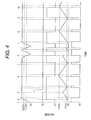
- Fig. 4 is a graph showing an operation state of the monitoring circuit illustrated in Fig. 3, and (a) indicates a
source voltage 8b, (b) indicates a normal operation clock sent from amicrocomputer 7, (c) indicates a rest signal sent from acomparator 5 and awindow comparator 4 to the microcomputer 7 (reset with LOW), (d) indicates an amount of electric charges of acapacitor 3 which is measured by thewindow comparator 4, and (e) indicates an output of thewindow comparator 4. - For the designations in the drawings, 1 denotes a charging circuit, 2a denotes a constant current source, 2b denotes an N-type MOS transistor, 3 denotes a capacitor, 4 denotes a window comparator, 5 denotes a comparator, 6 and 9 denote a logic circuit, 7 denotes a microcomputer, 8a and 8b denote a source voltage, 10a, 10b and 10c denote a resistor, and 16 denotes a monitoring circuit.
- Fig. 1 shows a
monitoring circuit 15 according to a structure of the invention. In Fig. 1, acurrent source 1 to be a charging circuit and acurrent source 2a to be a discharging circuit are connected to acapacitor 3, and thecapacitor 3 is connected to an input terminal of awindow comparator 4. For a threshold of thewindow comparator 4, an electric potential applied from asource voltage 8a is divided byresistors logic circuit 6 is operated in order to/not to transmit a reset output of thewindow comparator 4 to amicrocomputer 7. Furthermore, a source voltage of themicrocomputer 7 is also monitored in acomparator 5, and at the same time, a reset signal is output from thecomparator 5 to themicrocomputer 7 in a decrease in an electricity of themicrocomputer 7 and a trigger signal for discharging an electric charge of thecapacitor 3 is transmitted to alogic circuit 9. - An operation of a
monitoring circuit 15 will be described with reference to Fig. 2. In Fig. 2, an axis of ordinate indicates a voltage and an axis of abscissa indicates a time. In graphs of Fig. 2, (a) indicates asource voltage 8b, (b) indicates a normal operation clock sent from themicrocomputer 7, (c) indicates a reset signal sent from thecomparator 5 and thewindow comparator 4 to the microcomputer 7 (reset with LOW), (d) indicates an amount of electric charges of thecapacitor 3 which is measured by thewindow comparator 4, and (e) indicates an output of thewindow comparator 4. - A vertical line (1) in Fig. 2 indicates a timing in which the
monitoring circuit 15 and themicrocomputer 7 according to the invention shown in Fig. 1 are turned on. - A vertical line (2) in Fig. 2 indicates a timing in which the
source voltage 8b is higher than a threshold voltage (VDDthh) on the HIGH side of thecomparator 5 so that thecharging circuit 1 is activated to start to store electric charges in thecapacitor 3. At this time, moreover, themicrocomputer 7 is brought into a reset release state. - A vertical line (3) in Fig. 2 indicates a timing of an input of a normal operation clock from the
microcomputer 7 which is to be input to thelogic circuit 9 of themonitoring circuit 15 when themicrocomputer 7 is operated normally. When the normal operation clock sent from themicrocomputer 7 is input to thelogic circuit 9, thecharging circuit 1 is stopped so that thedischarging circuit 2a is activated. Therefore, the electric charges of thecapacitor 3 are discharged. - A vertical line (4) in Fig. 2 indicates a timing in which the electric charge of the
capacitor 3 which is measured by thewindow comparator 4 is higher than a threshold voltage (VCthh) on the HIGH side of thewindow comparator 4. When themicrocomputer 7 is not operated normally, the normal operation clock sent from themicrocomputer 7 is not input to a logic circuit constituting a conventional monitoring circuit. Consequently, this state is brought. At this time, the output HIGH (H) of thewindow comparator 4 resets themicrocomputer 7 through thelogic circuit 6. Furthermore, thecharging circuit 1 is stopped by the output H of thewindow comparator 4 and thecharging circuit 2a is activated. - A vertical line (5) in Fig. 2 indicates a timing in which the electric charge of the
capacitor 3 which is measured by thewindow comparator 4 is lower than a threshold voltage (VCthl) on the LOW side of thewindow comparator 4. At this time, the output of thewindow comparator 4 is HIGH so that the output of thewindow comparator 4 stops thedischarging circuit 2a through thelogic circuits charging circuit 1 is activated. - A vertical line (6) in Fig. 2 indicates a timing in which the
source voltage 8b is lower than a threshold voltage on the LOW side of the comparator 5 (a voltage VDDthl required for safely operating the microcomputer 7) for some reason. At this time, themicrocomputer 7 is brought into a reset state in response to the output of thecomparator 5. - As described above, the
monitoring circuit 15 shown in Fig. 1 has such a structure that the microcomputer is reset when the source voltage is lower than the necessary voltage for the safe operation of the microcomputer, and the microcomputer is not decided to be operated normally and the microcomputer is thus reset when the normal operation clock sent from the microcomputer is not input to the monitoring circuit for a certain period. - According to the embodiment, it is possible to safely reset the microcomputer also in a decrease in a power of the microcomputer.
- In the
monitoring circuit 15 according to the invention shown in Fig. 1, a reset release section of themicrocomputer 7 is varied in such a manner that lengths of a section between a vertical line (7) and a vertical line (8) and a section between a vertical line (9) and a vertical line (10) in Fig. 2 are different from each other. This is a phenomenon caused by constraints in respect of a structure of a circuit, that is, themicrocomputer 7 is reset in response to the output of thewindow comparator 4 only when the electric charge of thecapacitor 3 is higher than the threshold voltage on the HIGH side of thewindow comparator 4 in the case in which thesource voltage 8b is continuously normal and in which the normal operation clock sent from themicrocomputer 7 is not input to the monitoring circuit for a certain period as shown in a one-dotted chain line A in Fig. 2 illustrating a voltage waveform of themonitoring circuit 15 according to the invention in Fig. 1. More specifically, the reason why the different section is observed in the reset release section of themicrocomputer 7 is that there is no means for resetting themicrocomputer 7 other than the output of thewindow comparator 4 when thesource voltage 8b is normal. - In order to measure a time that the normal operation clock to be output in the normal operation of the
microcomputer 7 does not reach the monitoring circuit when thesource voltage 8b is normal, however, it is necessary to employ a structure in which themicrocomputer 7 is reset only when the electric charge of thecapacitor 3 in the monitoring circuit shown in Fig. 1 is higher than the threshold voltage on the HIGH side of thewindow comparator 4 as shown in the one-dotted chain line A of Fig. 2. - In some cases in which the
source voltage 8b is recovered and exceeds the threshold voltage on the HIGH side of thecomparator 5 when the electric charge of thecapacitor 3 is increased to some extent as shown in the vertical line (7) of Fig. 2, moreover, a signal for releasing the reset of themicrocomputer 7 is output from thewindow comparator 4 or thelogic circuit 6. As long as the source voltage is normal, the reset release signal is maintained in that state until the electric charge of thecapacitor 3 exceeds the threshold voltage on the HIGH side of thewindow comparator 4. - From the foregoing, in the
monitoring circuit 15 according to the invention shown in Fig. 1, there is made an imbalance that the different reset release section of themicrocomputer 7 is generated in such a manner that the section between the vertical line (7) and the vertical cline (8) and the section between the vertical line (9) and the vertical line (10) in Fig. 2 have lengths which are different from each other. - A
monitoring circuit 16 shown in Fig. 3 according to a second embodiment of the invention serves to correct the unbalanced reset release section. In contrast to themonitoring circuit 15 shown in Fig. 1, the monitoring circuit according to the embodiment is provided with adischarging circuit 2b to be new discharging means and serves to discharge the electric charge of acapacitor 3 by a switching operation. - The
monitoring circuit 16 according to the invention shown in Fig. 3 measures an arrival interval of a normal operation clock for monitoring asource voltage 8b (VDD) of amicrocomputer 7 to be a monitoring object to safely end themicrocomputer 7 in a decrease in a power in which thesource voltage 8b is lower than a source voltage to safely operate themicrocomputer 7 and for resetting themicrocomputer 7 when a period for which themicrocomputer 7 is not operated normally exceeds a certain period of time. Thesource voltage 8b of themicrocomputer 7 is monitored by using acomparator 5 to be source voltage deciding means. Moreover, an interval between the normal operation clocks is monitored by controlling acharging circuit 1 to be charging means, and a dischargingcircuit 2a and a dischargingcircuit 2b which are discharging means to measure a voltage stored in thecapacitor 3 through awindow comparator 4 to be voltage comparing means, thereby creating a certain time to observe the arrival of the normal operation clock. Accordingly, themicrocomputer 7 is not continuously operated without resetting in the decrease in a power but when the normal operation clock is input to the conventional monitoring circuit shown in Fig. 1. In Fig. 3, asource voltage 8a which is different from that of themicrocomputer 7 is used for the source voltage of the monitoring circuit. - The operation of the monitoring circuit according to the invention shown in Fig. 3 will be described below with reference to a voltage fluctuation chart for the monitoring circuit according to the invention illustrated in Fig. 4. In Fig. 4, an axis of ordinate indicates a voltage and an axis of abscissa indicates a time. In graphs shown in Fig. 4, (a) indicates the
source voltage 8b, (b) indicates a normal operation clock sent from themicrocomputer 7, (c) indicates a reset signal sent from thecomparator 5 to the microcomputer 7 (a reset state with LOW), (d) indicates an amount of electric charges of thecapacitor 3 which is measured by thewindow comparator 4, and (e) indicates an output of thewindow comparator 4. - A vertical line (1) in Fig. 4 indicates a timing in which the conventional monitoring circuit and the
microcomputer 7 shown in Fig. 3 are turned on. - A vertical line (2) in Fig. 4 indicates a timing in which the
source voltage 8b is higher than a threshold voltage (VDDthh) on the HIGH side of thecomparator 5 so that the chargingcircuit 1 is activated to start to store electric charges in thecapacitor 3. At this time, moreover, themicrocomputer 7 is brought into a reset releasestate. Although the threshold voltage on the HIGH side of thecomparator 5 and a threshold voltage (VDDthl) on the LOW side of thecomparator 5 which will be described below are set to have a hysteresis by feeding back the output of thecomparator 5 to make a division through a resistor, this means is not restricted. - A vertical line (3) in Fig. 4 indicates a timing of an input of a normal operation clock from the
microcomputer 7 which is to be input to alogic circuit 9 of the monitoring circuit according to the invention shown in Fig. 3 when themicrocomputer 7 is operated normally. When the normal operation clock sent from themicrocomputer 7 is input to thelogic circuit 9, the chargingcircuit 1 is stopped so that the dischargingcircuit 2a is activated. Therefore, the electric charges of thecapacitor 3 are discharged. - A vertical line (4) in Fig. 4 indicates a timing in which a charging voltage of the
capacitor 3 which is measured by thewindow comparator 4 is higher than a threshold voltage (VCthh) on the HIGH side of thewindow comparator 4. If the normal operation clock sent from themicrocomputer 7 is not input to the monitoring circuit according to the invention, this state is brought. At this time, the output HIGH (H) of thewindow comparator 4 resets themicrocomputer 7 through alogic circuit 6. Furthermore, the chargingcircuit 1 is stopped by the output H of thewindow comparator 4 and the chargingcircuit 2a is activated. The threshold voltage on the HIGH side of thewindow comparator 4 and a threshold voltage (VCthl) on the LOW side of thewindow comparator 4 which will be described below are set by dividing asource voltage 8a of thewindow comparator 4 throughresistors - A vertical line (5) in Fig. 4 indicates a timing in which the electric charge of the
capacitor 3 which is measured by thewindow comparator 4 is lower than the threshold voltage (VCthl) on the LOW side of thewindow comparator 4. At this time, the dischargingcircuit 2a is stopped in response to the output of thewindow comparator 4, and furthermore, the chargingcircuit 1 is activated. - A vertical line (6) in Fig. 4 indicates a timing in which the
source voltage 8b is lower than a threshold voltage (VDDthl) on the LOW side of thecomparator 5 due to a fluctuation in a load or a noise. At this time, themicrocomputer 7 is reset in response to the output of thecomparator 5, and furthermore,thedischargingcircuit 2b is activated in response to the output of thecomparator 5, thereby discharging the electric charge of thecapacitor 3. - As described above, the
monitoring circuit 16 according to the invention shown in Fig. 3 is operated in such a manner that themicrocomputer 7 is reset in response to the output of thewindow comparator 4 when the electric charge of thecapacitor 3 is stored and a voltage detected by thewindow comparator 4 is raised to exceed the threshold voltage on the HIGH side of thewindow comparator 4, and themicrocomputer 7 is reset in response to the output of thecomparator 5 when thesource voltage 8b is lower than the threshold voltage on the LOW side of thecomparator 5. More specifically, the monitoring circuit according to the invention serves to monitor both the interval between the normal operation clocks of themicrocomputer 7 and thesource voltage 8b of themicrocomputer 7. - The monitoring circuit according to the invention has such a structure that the electric charge of the capacitor is discharged every time the source voltage of the monitoring object is reduced by a constant amount or more in a decrease in a power. In a voltage waveform diagram of Fig. 4 for the monitoring circuit according to the invention illustrated in Fig. 3, consequently, a reset release section between a vertical line (7) and a vertical line (8) is almost equal to a reset release section between a vertical line (9) and a vertical line (10) as compared with the voltage waveform diagram of Fig. 2 for the
monitoring circuit 15 illustrated in Fig. 1. By maintaining the section of the reset release state of the microcomputer to have a constant length, it is possible to generate a reset signal in a desirable timing. Therefore, it is possible to eliminate a time loss before resetting the microcomputer. Furthermore, it is possible to cause the control of an electronic apparatus comprising the microcomputer to be more accurate. - While the invention has been described in detail with reference to the specific embodiments, it is apparent to the skilled in the art that various changes and modifications can be made without departing from the spirit and scope of the invention.
- The monitoring circuit according to the invention is sealed simply or together with other integrated circuits so as to be a semiconductor device, and the semiconductor device is mounted on an electronic apparatus together with a microcomputer to be a monitoring object. The electronic apparatus indicates every electric product comprising a microcomputer such as a television or a refrigerator.
- The invention is not restricted to the embodiments but all designs and changes within the range of matters described in claims are included in the scope of the invention. For example, an analog switch may be used in place of the
NMOS 2b. Even if a hysteresis comparator is used in place of thewindow comparator 4, it is possible to achieve the same object.
Claims (8)
- A monitoring circuit comprising a capacitor, charging means for charging the capacitor, discharging means for discharging the capacitor, voltage comparing means for comparing a certain reference voltage with a charging voltage of the capacitor, thereby generating a signal for resetting an operation of a monitoring object when the capacitor is charged to have a certain voltage or more, and source voltage deciding means for monitoring a source voltage of the monitoring object and resetting the operation of the monitoring object when the source voltage of the monitoring object is equal to or lower than a certain voltage.
- A monitoring circuit comprising a capacitor, charging means for charging the capacitor, first discharging means for discharging the capacitor, second discharging means for discharging the capacitor, voltage comparing means for comparing a certain reference voltage with a voltage of the capacitor, thereby generating a signal for resetting an operation of a monitoring object when the capacitor is charged to have a certain voltage or more, and source voltage deciding means for monitoring a source voltage of the monitoring object and resetting the operation of the monitoring object when the source voltage of the monitoring object is equal to or lower than a certain voltage.
- The monitoring circuit according to claim 1 or 2, wherein the source voltage deciding means is constituted by a comparator and the charging means is constituted by a current source.
- The monitoring circuit according to claim 2 or 3, wherein the first discharging means is constituted by a current source and the second discharging means is constituted by an analog switch, and either or both of the first and second discharging means is/are operated to invert an output of the voltage comparingmeans, thereby resetting the monitoring object when the source voltage of the monitoring obj ect is equal to or lower than a certain voltage.
- The monitoring circuit according to claim 2 or 3, wherein the first discharging means is constituted by a current source and the second discharging means is constituted by an N-type MOS transistor.
- The monitoring circuit according to claim 1 or 2, wherein the voltage comparing means is constituted by a window comparator.
- The monitoring circuit according to claim 1 or 2, wherein the voltage comparing means is constituted by a hysteresis comparator.
- A semiconductor device comprising the monitoring circuit according to claim 1 or 2 in which the capacitor is provided on an outside of the semiconductor device.
Applications Claiming Priority (3)
| Application Number | Priority Date | Filing Date | Title |
|---|---|---|---|
| JP2003432797 | 2003-12-26 | ||
| JP2004285617 | 2004-09-30 | ||
| PCT/JP2004/019485 WO2005066742A1 (en) | 2003-12-26 | 2004-12-20 | Monitoring circuit |
Publications (1)
| Publication Number | Publication Date |
|---|---|
| EP1710661A1 true EP1710661A1 (en) | 2006-10-11 |
Family
ID=34752059
Family Applications (1)
| Application Number | Title | Priority Date | Filing Date |
|---|---|---|---|
| EP04807840A Withdrawn EP1710661A1 (en) | 2003-12-26 | 2004-12-20 | Monitoring circuit |
Country Status (6)
| Country | Link |
|---|---|
| US (1) | US20080141053A1 (en) |
| EP (1) | EP1710661A1 (en) |
| JP (1) | JPWO2005066742A1 (en) |
| KR (1) | KR20060124628A (en) |
| TW (1) | TW200528980A (en) |
| WO (1) | WO2005066742A1 (en) |
Families Citing this family (2)
| Publication number | Priority date | Publication date | Assignee | Title |
|---|---|---|---|---|
| US7948283B2 (en) * | 2008-01-23 | 2011-05-24 | Tritan Technology Inc. | Apparatus for awaking an electronic device from a standby mode |
| KR102677512B1 (en) * | 2018-08-07 | 2024-06-24 | 삼성전자주식회사 | Device including safety logic |
Family Cites Families (8)
| Publication number | Priority date | Publication date | Assignee | Title |
|---|---|---|---|---|
| JPH0776933B2 (en) * | 1987-08-10 | 1995-08-16 | 日本電装株式会社 | Reset device for digital computer |
| JPH02246612A (en) * | 1989-03-20 | 1990-10-02 | Yokogawa Electric Corp | Watchdog timer circuit |
| JP3380978B2 (en) * | 1994-12-15 | 2003-02-24 | 三菱電機株式会社 | Semiconductor device |
| JP3752022B2 (en) * | 1995-08-25 | 2006-03-08 | 株式会社デンソー | Electronic control unit with fault diagnosis function |
| JP3633092B2 (en) * | 1996-03-18 | 2005-03-30 | 日産自動車株式会社 | Microcomputer failure monitoring device |
| JPH1196044A (en) * | 1997-09-24 | 1999-04-09 | Denso Corp | Abnormality detection device and abnormality detection method for abnormality monitoring circuit |
| JP4365911B2 (en) * | 1998-11-11 | 2009-11-18 | 株式会社日立製作所 | Semiconductor integrated circuit |
| JP2001156610A (en) * | 1999-11-24 | 2001-06-08 | Nec Corp | Watchdog timer control circuit and watchdog timer control method |
-
2004
- 2004-12-20 JP JP2005516846A patent/JPWO2005066742A1/en active Pending
- 2004-12-20 WO PCT/JP2004/019485 patent/WO2005066742A1/en not_active Ceased
- 2004-12-20 KR KR1020067011634A patent/KR20060124628A/en not_active Ceased
- 2004-12-20 US US10/583,744 patent/US20080141053A1/en not_active Abandoned
- 2004-12-20 EP EP04807840A patent/EP1710661A1/en not_active Withdrawn
- 2004-12-22 TW TW093139958A patent/TW200528980A/en unknown
Non-Patent Citations (1)
| Title |
|---|
| See references of WO2005066742A1 * |
Also Published As
| Publication number | Publication date |
|---|---|
| TW200528980A (en) | 2005-09-01 |
| JPWO2005066742A1 (en) | 2007-12-20 |
| KR20060124628A (en) | 2006-12-05 |
| WO2005066742A1 (en) | 2005-07-21 |
| US20080141053A1 (en) | 2008-06-12 |
Similar Documents
| Publication | Publication Date | Title |
|---|---|---|
| JP5362996B2 (en) | Protective device and its electric quantity detection method | |
| US6437541B1 (en) | Battery state monitoring circuit and battery device | |
| KR100562877B1 (en) | Charge / discharge control circuit and charging type power supply | |
| JP3296385B2 (en) | Battery voltage detection circuit | |
| US9246323B2 (en) | Current controller and protection circuit | |
| CN110098597B (en) | Drive circuit with overcurrent protection function | |
| US9622304B2 (en) | Load driving circuit | |
| CN110780208B (en) | Apparatus and method for monitoring battery and storing data based on battery status | |
| US10069493B2 (en) | Circuitry and method for operating an electronic switch | |
| US7135937B2 (en) | Oscillator circuit and integrated circuit incorporating the same | |
| CA2250675C (en) | On/off control device for power source unit | |
| US11555847B2 (en) | Semiconductor integrated circuit device | |
| EP0933863A2 (en) | Electronic instrument | |
| EP1710661A1 (en) | Monitoring circuit | |
| EP4336730B1 (en) | Multi-function control circuit and pre-circuit configuration | |
| CN115173365B (en) | Control method of overvoltage protection device and overvoltage protection device | |
| JPH10257799A (en) | Output open detection device of multi-channel output device | |
| US11563430B2 (en) | Transistor diagnostic circuit | |
| JP2007214647A (en) | High side drive circuit | |
| US6084961A (en) | Circuit for monitoring battery voltages of telephone terminal facility, using power detector temporarily activated by ringing or off-hook signal | |
| US20040228054A1 (en) | Fault detecting circuit | |
| JPH116885A (en) | Electronic equipment with power generation means | |
| US20250373032A1 (en) | Fast switch-off circuit for charging tube of battery management system | |
| JPH073943B2 (en) | Overcurrent protection circuit | |
| JP7710355B2 (en) | Battery-less sensor circuit. |
Legal Events
| Date | Code | Title | Description |
|---|---|---|---|
| PUAI | Public reference made under article 153(3) epc to a published international application that has entered the european phase |
Free format text: ORIGINAL CODE: 0009012 |
|
| 17P | Request for examination filed |
Effective date: 20060626 |
|
| AK | Designated contracting states |
Kind code of ref document: A1 Designated state(s): DE FR GB NL |
|
| DAX | Request for extension of the european patent (deleted) | ||
| RBV | Designated contracting states (corrected) |
Designated state(s): DE FR GB NL |
|
| STAA | Information on the status of an ep patent application or granted ep patent |
Free format text: STATUS: THE APPLICATION HAS BEEN WITHDRAWN |
|
| 18W | Application withdrawn |
Effective date: 20091124 |