EP1705726A2 - Ambipolar organic thin-film field-effect transistor and its fabrication method - Google Patents
Ambipolar organic thin-film field-effect transistor and its fabrication method Download PDFInfo
- Publication number
- EP1705726A2 EP1705726A2 EP06251639A EP06251639A EP1705726A2 EP 1705726 A2 EP1705726 A2 EP 1705726A2 EP 06251639 A EP06251639 A EP 06251639A EP 06251639 A EP06251639 A EP 06251639A EP 1705726 A2 EP1705726 A2 EP 1705726A2
- Authority
- EP
- European Patent Office
- Prior art keywords
- transistor
- organic compound
- insulator layer
- organic
- layer
- Prior art date
- Legal status (The legal status is an assumption and is not a legal conclusion. Google has not performed a legal analysis and makes no representation as to the accuracy of the status listed.)
- Granted
Links
Images


Classifications
-
- H—ELECTRICITY
- H10—SEMICONDUCTOR DEVICES; ELECTRIC SOLID-STATE DEVICES NOT OTHERWISE PROVIDED FOR
- H10K—ORGANIC ELECTRIC SOLID-STATE DEVICES
- H10K10/00—Organic devices specially adapted for rectifying, amplifying, oscillating or switching; Organic capacitors or resistors having potential barriers
- H10K10/40—Organic transistors
- H10K10/46—Field-effect transistors, e.g. organic thin-film transistors [OTFT]
- H10K10/462—Insulated gate field-effect transistors [IGFETs]
- H10K10/468—Insulated gate field-effect transistors [IGFETs] characterised by the gate dielectrics
- H10K10/471—Insulated gate field-effect transistors [IGFETs] characterised by the gate dielectrics the gate dielectric comprising only organic materials
-
- H—ELECTRICITY
- H10—SEMICONDUCTOR DEVICES; ELECTRIC SOLID-STATE DEVICES NOT OTHERWISE PROVIDED FOR
- H10K—ORGANIC ELECTRIC SOLID-STATE DEVICES
- H10K10/00—Organic devices specially adapted for rectifying, amplifying, oscillating or switching; Organic capacitors or resistors having potential barriers
- H10K10/40—Organic transistors
- H10K10/46—Field-effect transistors, e.g. organic thin-film transistors [OTFT]
- H10K10/462—Insulated gate field-effect transistors [IGFETs]
- H10K10/466—Lateral bottom-gate IGFETs comprising only a single gate
-
- H—ELECTRICITY
- H10—SEMICONDUCTOR DEVICES; ELECTRIC SOLID-STATE DEVICES NOT OTHERWISE PROVIDED FOR
- H10K—ORGANIC ELECTRIC SOLID-STATE DEVICES
- H10K85/00—Organic materials used in the body or electrodes of devices covered by this subclass
- H10K85/30—Coordination compounds
- H10K85/311—Phthalocyanine
Definitions
- This invention relates to a thin-film field-effect transistor (TFT) having a metal/insulator/semiconductor (MIS) structure and more particularly, to such a TFT which uses an organic compound having dielectric properties, especially hysteresis similar to ferroelectric material as the insulator layer, and exhibits both p- and n-type transistor characteristics; and a method for preparing the same.
- TFT thin-film field-effect transistor
- MIS metal/insulator/semiconductor
- TFTs thin-layer field-effect transistors
- silicon semiconductor or compound semiconductor are used in general integrated circuits and other expanding applications. While the number of new applications to which such devices are desirably applied is increasing, the requirements of lower cost and flexibility are imposed on these devices. To comply with such requirements, active research works have been made on organic semiconductors because of possible fabrication of devices having a variety of functions including low cost and flexibility. The implementation of organic semiconductors into a commercial practice will lead to the appearance of printable integrated circuits, electronic paper and the like. However, most organic semiconductors exhibit p-type behavior while only C60 and few other materials exhibit n-type behavior. N-type organic semiconductors are key materials for the establishment of organic electronic devices including p-n junctions.
- organic semiconductors are not prone to polarity inversion from p-type to n-type, because they have so great a band gap as compared with silicon semiconductor that no inversion layer is formed even when the band is deflected by applying an extra gate voltage.
- the inversion layer may be formed by inducing numerous carriers at the interface between the gate insulating film and the organic semiconductor, a high gate voltage can cause breakdown if a prior art gate insulating film is used. It is thus difficult to induce a sufficient quantity of carriers to provoke polarity inversion.
- Appl. Phys. Lett., Vol. 85, p3899 (2004 ) describes to use an aluminum oxide thin film having a high withstand voltage, high dielectric constant and low leakage current as the insulating film and a single crystal as the organic semiconductor. Allegedly the use of a single crystal as the organic semiconductor eliminates the influence of grains and trap level in the semiconductor thin film, and it is thus expected to gain a high mobility.
- the oxide insulator has the advantages of ease of thin film formation and a high dielectric constant, it undesirably has a low withstand voltage due to the essential presence of oxygen vacancies.
- An object of the present invention is to provide an ambipolar organic thin-film field-effect transistor which exhibits both p- and n-type transistor characteristics while it can be prepared in a relatively simple manner, and a method for preparing the same.
- an ambipolar organic thin-film field-effect transistor is obtainable in a relatively simple manner which exhibits both p- and n-type transistor characteristics in that the transistor exhibits n-type transistor characteristics when polling is conducted by applying a voltage which is not less than a coercive electric field and not more than a withstand voltage of the organic compound of the insulator layer between source and gate electrodes, and absent polling, the transistor exhibits p-type transistor characteristics.
- the present invention provides an ambipolar organic thin-film field-effect transistor having metal/insulator/semiconductor structure, wherein the material of which the semiconductor layer is made comprises an organic compound, and the material of which the insulator layer is made comprises an organic compound which is soluble in an organic solvent and exhibits spontaneous polarization of ferroelectric type, the transistor exhibits n-type transistor characteristics when polling is conducted by applying a voltage which is not less than a coercive electric field and not more than a withstand voltage of the organic compound of the insulator layer between source and gate electrodes, and the transistor exhibits p-type transistor characteristics when polling is not conducted.
- the organic compound of which the insulator layer is made is a polymer having a weight average molecular weight of 2,500 to 1,000,000.
- the organic compound of which the insulator layer is made is an insulating polymer having cyano groups, typically an insulating polymer having cyanoethyl groups, and more typically cyanoethylpullulan.
- the organic compound of the insulator layer has a withstand voltage of at least 1 MV/cm, a coercive electric field of at least 50 kV/cm, and a spontaneous polarization Pr of at least 1.5 ⁇ C/cm 2 .
- the invention provides a method for preparing an ambipolar organic thin-film field-effect transistor, comprising the steps of applying a solution of an organic solvent-soluble organic compound in an organic solvent onto a gate electrode in the form of a metal layer, drying the applied solution to form an insulator layer, and laying a semiconductor layer on the insulator layer.
- TFTs thin-film field-effect transistors
- MIS metal/insulator/semiconductor
- the transistor of the invention can be almost prepared by a solvent-basis process since the semiconductor and insulator layers are formed of organic compounds. Namely the transistor of the invention can be prepared simply by a printing technique like ink jet printing, leading to a reduced cost of manufacture.
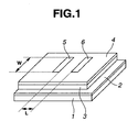
- an ambipolar organic thin-film field-effect transistor embodying the invention is shown as comprising a substrate 1 of SiO 2 or the like, a metal layer 2 formed on the substrate 1 and serving as a gate electrode, an insulator layer 3 formed on the metal layer 2, and a semiconductor layer 4 formed on the insulator layer 3. Source and drain electrodes 5 and 6 are formed on the semiconductor layer 4.
- Examples of substrate include glass and a polymer sheet.
- the metal layer used herein may be a conventional indium tin oxide (ITO) film, or a single metal layer such as Au, Cu or Al or a metal layer laminate such as Au/Ti, Cu/Ti or Al/Ti which is formed by physical vapor deposition (PVD) or metal organic chemical vapor deposition (MOCVD). Since a possibility of film formation by printing is advantageous to the objects herein, the use of conductive metal paste is preferred as long as it raises no practical problems.
- ITO indium tin oxide
- MOCVD metal organic chemical vapor deposition
- the polarity inversion phenomenon of semiconductor largely depends on the band alignment between semiconductor and insulator and the quantity of charge accumulated at the interface, the insulator's properties are more predominant from the standpoint of polarity inversion. Accordingly, a thin film that offers transistor performance and can accumulate giant charges at the interface is desired for polarity inversion.
- organic insulating materials generally have a high withstand voltage and deliver low leakage current.
- oxygen vacancies are not avoidable in an aluminum oxide thin film as the insulator film.
- molecular vacancies exist in organic compounds. While oxygen vacancies associated with oxides can alter the electronic state of an insulator, molecular vacancies in organic compounds are not correlated to the electronic state. Then the organic compounds deliver low leakage current.
- the organic insulating material cannot accumulate a multiplicity of charges at the interface due to a low dielectric constant.
- the inventors have found that use of a specific organic compound having a high withstand voltage and a high dielectric constant as the insulator layer-forming material enables to construct an ambipolar organic thin-film field-effect transistor exhibiting both p- and n-type transistor characteristics.
- the material of which the insulator layer is made is typically an organic compound which is soluble in an organic solvent and exhibits spontaneous polarization similar to ferroelectric material.
- the preferred organic compound has a withstand voltage of at least 1 MV/cm, a coercive electric field of at least 50 kV/cm, and a spontaneous polarization Pr of at least 1.5 ⁇ C/cm 2 .
- the organic compound is preferably a high molecular weight compound or polymer having a weight average molecular weight (Mw) of 2,500 to 1,000,000 as measured by gel permeation chromatography (GPC) relative to polystyrene standards. It is preferably an insulating polymer having cyano groups, especially cyanoethyl groups. Examples include cyanoethylpullulan, cyanoethylated dihydroxypropylpullulan, cyanoethyl cellulose, cyanoethyl polyvinyl alcohol, and polyacrylonitrile, with cyanoethylpullulan being most preferred.
- the insulating polymer having cyano groups for example, cyanoethylpullulan is obtainable by reacting a pullulan resin (consisting of polysaccharides produced by microorganisms) with acrylonitrile in the presence of an alkali catalyst for substituting cyanoethyl groups for the hydroxyl groups on the pullulan resin (see JP-B 59-31521 ). Since cyano groups introduced in side chains (cyanoethyl groups in the case of cyanoethylpullulan) have a great polar moment, a more amount of cyano groups introduced leads to a higher dielectric constant (relative permittivity) and hence, a reduction of dielectric loss which is a loss factor.
- cyanoethylpullulan is obtainable by reacting a pullulan resin (consisting of polysaccharides produced by microorganisms) with acrylonitrile in the presence of an alkali catalyst for substituting cyano
- the insulating polymer having cyano groups preferably has a percent substitution with cyano groups (in the case of cyanoethylpullulan, a percent substitution of hydroxyl groups on pullulan resin with cyanoethyl groups) of at least 80 mol%, and more preferably at least 85 mol%.
- the upper limit, which is not critical, is theoretically 100 mol%.
- Cyanoethylpullulan with a percent substitution in this range has a dielectric constant of 19 at 100 Hz to 1 kHz which is very high among polymers, and also has a high withstand voltage of at least 1 MV/cm. Then it is a dielectric material having excellent insulating properties.
- the material of which the semiconductor layer is made is an organic compound.
- suitable organic compounds for forming the semiconductor layer include low molecular weight compounds such as pentacene, metal phthalocyanine such as copper phthalocyanine and iron phthalocyanine, and ⁇ -sexithienyl; and high molecular weight compounds such as polythiophenes, polypyrroles, polyanilines, polyacetylenes, poly(thienylene vinylene)s, and poly(phenylene vinylene)s.
- low molecular weight compounds such as pentacene, metal phthalocyanine such as copper phthalocyanine and iron phthalocyanine, and ⁇ -sexithienyl
- high molecular weight compounds such as polythiophenes, polypyrroles, polyanilines, polyacetylenes, poly(thienylene vinylene)s, and poly(phenylene vinylene)s.
- low molecular weight compounds such as pentacene,
- the semiconductor layer prefers an organic solvent-soluble polymer having a weight average molecular weight (Mw) of 2,000 to 1,000,000 as measured by GPC relative to polystyrene standards.
- Mw weight average molecular weight
- the preferred polymer include polythiophenes, polypyrroles, polyanilines, polyacetylenes, poly(thienylene vinylene)s, and poly(phenylene vinylene)s.
- polythiophenes typically poly(3-hexylthiophene) are most preferred.
- a solution coating/drying process may be employed to lay the semiconductor layer on the insulator layer.
- the organic compound for forming the semiconductor layer should be dissolved in an organic solvent in which the insulator layer is not dissolvable. This is because it is generally believed that when a semiconductor layer and an insulator layer are formed by such solution coating lamination, the interface state does not become uniform.
- organic compound for forming the insulator layer is an insulating polymer having cyano groups
- suitable organic solvents in which it is dissolved include N-methyl-2-pyrrolidone, N,N'-dimethylformamide, acetone, acetonitrile, and ⁇ -butyrolactone.
- the other organic solvent in which the compound for forming the semiconductor layer is dissolved is the solvent in which the insulating polymer having cyano groups is not dissolvable, for example, chloroform, toluene, hexane and alcohols. In either case, one or more solvents may be used.
- the ambipolar organic thin-film field-effect transistor can be manufactured by well-known methods.
- a substrate is selected from glass and conventional polymer sheets.
- a metal layer serving as the gate electrode is formed on the substrate by sputtering or by applying a metal paste or conductive polymer through spin coating, screen printing or ink jet printing, and drying.
- commercially available ITO-coated glass may be used.
- a solution of the insulator layer-forming material in an organic solvent is coated by spin coating, screen printing or ink jet printing, and dried, thus forming an insulator layer.
- a solution of the semiconductor layer-forming material in another organic solvent (in which the insulator layer-forming material is not dissolvable) is coated onto the insulator layer by spin coating, screen printing or ink jet printing, and dried to form a semiconductor layer.
- the material is evaporated in vacuum to deposit a semiconductor layer.
- the surface of the insulator layer may be subjected to well-known rubbing or physical treatment in order that semiconductor molecules be oriented at the interface between the insulator layer and the semiconductor layer.
- source and drain electrodes are formed on the semiconductor layer by sputtering or by applying a metal paste or conductive polymer through screen printing or ink jet printing, and drying.
- the insulator layer have a thickness of 0.2 to 10 ⁇ m, more preferably 0.5 to 3 ⁇ m, and the semiconductor layer have a thickness of 50 to 300 nm, more preferably 50 to 100 nm.
- the metal layer has a thickness of 30 to 50 nm.
- the transistor exhibits n-type transistor characteristics when polling is conducted by applying a voltage which is not less than the coercive electric field and not more than the withstand voltage of the organic compound of the insulator layer between source and gate electrodes, and the transistor exhibits p-type transistor characteristics when polling is not conducted.
- the material for forming the insulator layer was cyanoethylpullulan having a degree of substitution with cyanoethyl groups of 85.2 mol% (CyEPL, by Shin-Etsu Chemical Co., Ltd., CR-S, Mw: 49,000).
- the material for forming the semiconductor layer was copper phthalocyanine (Aldrich). Using these materials, an ambipolar organic thin-film field-effect transistor was fabricated by the following procedure and then tested.
- a gate electrode was formed by vapor depositing Ti to a thickness of 20 nm and then Au to a thickness of 60 nm, both by RF sputtering at room temperature and a back pressure of 10 -4 Pa.
- a 15 wt% solution of cyanoethylpullulan in N-methyl-2-pyrrolidone which had been passed through a 0.2- ⁇ m membrane filter was spin coated and dried at 100°C for one hour, forming an insulator layer of 2 ⁇ m thick.
- This insulator layer had an electrostatic capacity of 17.7 nF/cm 2 at 1 mHz.
- the substrate was cooled at -20°C, after which Au was deposited on the semiconductor layer to a thickness of 300 nm through a metal mask by RF sputtering at a back pressure of 10 -5 Pa or lower.
- the source and drain electrodes had a width W of 3.9 mm and were spaced a distance L of 38 ⁇ m (see FIG. 1).
- the FET thus fabricated was assessed for electrical characteristics under light-shielded condition and a vacuum of 1.3 ⁇ 10 -3 Pa or below.
- the source-drain current versus voltage I SD -V SD curves were measured at room temperature (25°C) and at different gate voltages. Typical p-type characteristics were observed at negative gate voltages. In the event of positive gate voltages, as the gate voltage increased, the source-drain current decreased and only a depletion layer formed.
- the applied gate voltage promoted depletion with the decreasing current value, but when the gate voltage exceeds 20 V, the device produced n-type transistor characteristics that an inversion layer is formed and the current value increases.
- the copper phthalocyanine layer is of p type and has a significant band gap of 1.5 eV, it takes a weakly inverted state despite a large amount of charges accumulated. For this reason, the n-type source-drain current value is as small as 1/2000 of the p-type source-drain current value (in the event
- 50 V).
- I SD (W/L) ⁇ [P+C(V SG -V T )]V SD is used wherein V T is the threshold voltage when the source-drain current rises.
- the p-type mobility was 4.1 ⁇ 10 -3 cm 2 /Vs, which is substantially equivalent to that of a field-effect transistor using silicon oxide as the gate insulating film.
- the field-effect mobility for the n-type was 3.5 ⁇ 10 -6 cm 2 /Vs which is about 1/1000 of that for the p-type.
- 10 V was 6 ⁇ 10 4 and 70, respectively, and the V T was -0.1 V and 0.9 V, respectively.
- the material for forming the insulator layer was cyanoethylpullulan having a degree of substitution with cyanoethyl groups of 85.2 mol% (CyEPL, by Shin-Etsu Chemical Co., Ltd., CR-S, Mw: 49,000).
- the material for forming the semiconductor layer was iron phthalocyanine (Aldrich). Using these materials, an ambipolar organic thin-film field-effect transistor was fabricated by the following procedure and then tested.
- a gate electrode was formed by vapor depositing Ti to a thickness of 20 nm and then Au to a thickness of 60 nm, both by RF sputtering at room temperature and a back pressure of 10 -4 Pa.
- a 15 wt% solution of cyanoethylpullulan in N-methyl-2-pyrrolidone which had been passed through a 0.2- ⁇ m membrane filter was spin coated and dried at 100°C for one hour, forming an insulator layer of 2 ⁇ m thick.
- This insulator layer had an electrostatic capacity of 17.7 nF/cm 2 at 1 mHz.
- the substrate was cooled at -20°C, after which Au was deposited on the semiconductor layer to a thickness of 300 nm through a metal mask by RF sputtering at a back pressure of 10 -5 Pa or lower.
- the source and drain electrodes had a width W of 3.9 mm and were spaced a distance L of 38 ⁇ m (see FIG. 1).
- the FET thus fabricated was assessed for electrical characteristics under light-shielded condition and a vacuum of 1.3 ⁇ 10 -3 Pa or below.
- the source-drain current versus voltage I SD -V SD curves were measured at room temperature (25°C) and at different gate voltages. Typical p-type characteristics were observed at negative gate voltages. In the event of positive gate voltages, as the gate voltage increased, the source-drain current decreased and only a depletion layer formed.
- the applied gate voltage promoted depletion with the decreasing current value, but when the gate voltage exceeds 60 V, the device produced n-type transistor characteristics that an inversion layer is formed and the current value increases.
- the iron phthalocyanine layer is of p type and has a significant band gap of 1.4 eV, it takes a weakly inverted state despite a large amount of charges accumulated. For this reason, the n-type source-drain current value is as small as 1/4000 of the p-type source-drain current value (in the event
- 80 V).
- I SD (W/L) ⁇ [P+C(V SG -V T )]V SD is used wherein V T is the threshold voltage when the source-drain current rises.
- the p-type mobility was 1.1 ⁇ 10 -4 cm 2 /Vs, which is substantially equivalent to that of a field-effect transistor using silicon oxide as the gate insulating film.
- the field-effect mobility for the n-type was 1.7x 10 -6 cm 2 /Vs which is about 1/65 of that for the p-type.
- 40 V was 3.5x10 3 and 70, respectively, and the V T was -4.3 V and 4.0 V, respectively.
Landscapes
- Chemical & Material Sciences (AREA)
- Inorganic Chemistry (AREA)
- Engineering & Computer Science (AREA)
- Materials Engineering (AREA)
- Thin Film Transistor (AREA)
- Insulated Gate Type Field-Effect Transistor (AREA)
Abstract
Description
- This invention relates to a thin-film field-effect transistor (TFT) having a metal/insulator/semiconductor (MIS) structure and more particularly, to such a TFT which uses an organic compound having dielectric properties, especially hysteresis similar to ferroelectric material as the insulator layer, and exhibits both p- and n-type transistor characteristics; and a method for preparing the same.
- Conventional thin-layer field-effect transistors (TFTs) utilizing silicon semiconductor or compound semiconductor are used in general integrated circuits and other expanding applications. While the number of new applications to which such devices are desirably applied is increasing, the requirements of lower cost and flexibility are imposed on these devices. To comply with such requirements, active research works have been made on organic semiconductors because of possible fabrication of devices having a variety of functions including low cost and flexibility. The implementation of organic semiconductors into a commercial practice will lead to the appearance of printable integrated circuits, electronic paper and the like. However, most organic semiconductors exhibit p-type behavior while only C60 and few other materials exhibit n-type behavior. N-type organic semiconductors are key materials for the establishment of organic electronic devices including p-n junctions.
- In general, organic semiconductors are not prone to polarity inversion from p-type to n-type, because they have so great a band gap as compared with silicon semiconductor that no inversion layer is formed even when the band is deflected by applying an extra gate voltage. Although the inversion layer may be formed by inducing numerous carriers at the interface between the gate insulating film and the organic semiconductor, a high gate voltage can cause breakdown if a prior art gate insulating film is used. It is thus difficult to induce a sufficient quantity of carriers to provoke polarity inversion.
- For instance, Appl. Phys. Lett., Vol. 85, p3899 (2004) describes to use an aluminum oxide thin film having a high withstand voltage, high dielectric constant and low leakage current as the insulating film and a single crystal as the organic semiconductor. Allegedly the use of a single crystal as the organic semiconductor eliminates the influence of grains and trap level in the semiconductor thin film, and it is thus expected to gain a high mobility. Although the oxide insulator has the advantages of ease of thin film formation and a high dielectric constant, it undesirably has a low withstand voltage due to the essential presence of oxygen vacancies.
- An object of the present invention is to provide an ambipolar organic thin-film field-effect transistor which exhibits both p- and n-type transistor characteristics while it can be prepared in a relatively simple manner, and a method for preparing the same.
- The inventors have discovered that by using an organic compound as the material of which the semiconductor layer is made and an organic compound which is soluble in an organic solvent and exhibits spontaneous polarization similar to ferroelectric material as the material of which the insulator layer is made, an ambipolar organic thin-film field-effect transistor is obtainable in a relatively simple manner which exhibits both p- and n-type transistor characteristics in that the transistor exhibits n-type transistor characteristics when polling is conducted by applying a voltage which is not less than a coercive electric field and not more than a withstand voltage of the organic compound of the insulator layer between source and gate electrodes, and absent polling, the transistor exhibits p-type transistor characteristics.
- Accordingly, the present invention provides an ambipolar organic thin-film field-effect transistor having metal/insulator/semiconductor structure, wherein the material of which the semiconductor layer is made comprises an organic compound, and the material of which the insulator layer is made comprises an organic compound which is soluble in an organic solvent and exhibits spontaneous polarization of ferroelectric type, the transistor exhibits n-type transistor characteristics when polling is conducted by applying a voltage which is not less than a coercive electric field and not more than a withstand voltage of the organic compound of the insulator layer between source and gate electrodes, and the transistor exhibits p-type transistor characteristics when polling is not conducted.
- In a preferred embodiment, the organic compound of which the insulator layer is made is a polymer having a weight average molecular weight of 2,500 to 1,000,000. In another preferred embodiment, the organic compound of which the insulator layer is made is an insulating polymer having cyano groups, typically an insulating polymer having cyanoethyl groups, and more typically cyanoethylpullulan. Preferably the organic compound of the insulator layer has a withstand voltage of at least 1 MV/cm, a coercive electric field of at least 50 kV/cm, and a spontaneous polarization Pr of at least 1.5 µC/cm2.
- In another aspect, the invention provides a method for preparing an ambipolar organic thin-film field-effect transistor, comprising the steps of applying a solution of an organic solvent-soluble organic compound in an organic solvent onto a gate electrode in the form of a metal layer, drying the applied solution to form an insulator layer, and laying a semiconductor layer on the insulator layer.
- By these means, we find that we are able to make thin-film field-effect transistors (TFTs) having metal/insulator/semiconductor (MIS) structure as explained above which produce n-type characteristics, presently otherwise unachievable by organic field-effect transistors using organic compounds to form the semiconductor and insulator layers. Thus it is an ambipolar organic thin-film field-effect transistor exhibiting both p- and n-type transistor characteristics. This feature allows the inventive transistor to find application in p-n junctions, inverter circuits and lasers.
- As opposed to the prior art field-effect transistors of MIS structure that require the photoresist processing steps including patterning and etching involved in the circuit-forming technology using metal-base semiconductor and insulator, the transistor of the invention can be almost prepared by a solvent-basis process since the semiconductor and insulator layers are formed of organic compounds. Namely the transistor of the invention can be prepared simply by a printing technique like ink jet printing, leading to a reduced cost of manufacture.
-
- FIG. 1 is a perspective view of an ambipolar organic thin-film field-effect transistor in one embodiment of the invention.
- FIG. 2 illustrates P-E curves of a cyanoethylpulluran film.
- FIG. 3 shows ISD-VSD curves at different gate voltages of an ambipolar organic thin-film field-effect transistor in Example 1 after polling, FIG. 3A corresponding to p-type transistor characteristics and FIG. 3B corresponding to n-type transistor characteristics.
- FIG. 4 shows ISD-VSD curves at different gate voltages of an ambipolar organic thin-film field-effect transistor in Example 2 after polling, FIG. 4A corresponding to p-type transistor characteristics and FIG. 4B corresponding to n-type transistor characteristics.
- Referring to FIG. 1, an ambipolar organic thin-film field-effect transistor embodying the invention is shown as comprising a
substrate 1 of SiO2 or the like, ametal layer 2 formed on thesubstrate 1 and serving as a gate electrode, aninsulator layer 3 formed on themetal layer 2, and asemiconductor layer 4 formed on theinsulator layer 3. Source anddrain electrodes semiconductor layer 4. - Examples of substrate include glass and a polymer sheet.
- The metal layer used herein may be a conventional indium tin oxide (ITO) film, or a single metal layer such as Au, Cu or Al or a metal layer laminate such as Au/Ti, Cu/Ti or Al/Ti which is formed by physical vapor deposition (PVD) or metal organic chemical vapor deposition (MOCVD). Since a possibility of film formation by printing is advantageous to the objects herein, the use of conductive metal paste is preferred as long as it raises no practical problems.
- Since the polarity inversion phenomenon of semiconductor largely depends on the band alignment between semiconductor and insulator and the quantity of charge accumulated at the interface, the insulator's properties are more predominant from the standpoint of polarity inversion. Accordingly, a thin film that offers transistor performance and can accumulate giant charges at the interface is desired for polarity inversion.
- The inventors learned that organic insulating materials generally have a high withstand voltage and deliver low leakage current. As previously pointed out, oxygen vacancies are not avoidable in an aluminum oxide thin film as the insulator film. Likewise, molecular vacancies exist in organic compounds. While oxygen vacancies associated with oxides can alter the electronic state of an insulator, molecular vacancies in organic compounds are not correlated to the electronic state. Then the organic compounds deliver low leakage current. The organic insulating material, however, cannot accumulate a multiplicity of charges at the interface due to a low dielectric constant. Continuing further investigations, the inventors have found that use of a specific organic compound having a high withstand voltage and a high dielectric constant as the insulator layer-forming material enables to construct an ambipolar organic thin-film field-effect transistor exhibiting both p- and n-type transistor characteristics.
- The material of which the insulator layer is made is typically an organic compound which is soluble in an organic solvent and exhibits spontaneous polarization similar to ferroelectric material. The preferred organic compound has a withstand voltage of at least 1 MV/cm, a coercive electric field of at least 50 kV/cm, and a spontaneous polarization Pr of at least 1.5 µC/cm2.
- The organic compound is preferably a high molecular weight compound or polymer having a weight average molecular weight (Mw) of 2,500 to 1,000,000 as measured by gel permeation chromatography (GPC) relative to polystyrene standards. It is preferably an insulating polymer having cyano groups, especially cyanoethyl groups. Examples include cyanoethylpullulan, cyanoethylated dihydroxypropylpullulan, cyanoethyl cellulose, cyanoethyl polyvinyl alcohol, and polyacrylonitrile, with cyanoethylpullulan being most preferred.
- The insulating polymer having cyano groups, for example, cyanoethylpullulan is obtainable by reacting a pullulan resin (consisting of polysaccharides produced by microorganisms) with acrylonitrile in the presence of an alkali catalyst for substituting cyanoethyl groups for the hydroxyl groups on the pullulan resin (see
JP-B 59-31521 - The insulating polymer having cyano groups preferably has a percent substitution with cyano groups (in the case of cyanoethylpullulan, a percent substitution of hydroxyl groups on pullulan resin with cyanoethyl groups) of at least 80 mol%, and more preferably at least 85 mol%. The upper limit, which is not critical, is theoretically 100 mol%. Cyanoethylpullulan with a percent substitution in this range has a dielectric constant of 19 at 100 Hz to 1 kHz which is very high among polymers, and also has a high withstand voltage of at least 1 MV/cm. Then it is a dielectric material having excellent insulating properties.
- An insulating film of cyanoethylpullulan was measured for dielectric properties at 1 mHz. Its P-E curve draws a hysteresis loop as shown in FIG. 2. The quantity (P) of charge associated with spontaneous polarization was Pr = 1.5 µC/cm2, and the coercive electric field was 50 kV/cm. In a linear region of the hysteresis loop between -10 kV/cm and 10 kV/cm, the film has a high electrostatic capacity C of 17.7 nF/cm2. The hysteresis loop of this P-E curve is similar to the ferroelectric material. Accordingly, in the structure using cyanoethylpullulan as the gate insulating film, for example, when polling is performed by applying a voltage (V) of equal to or more than the coercive electric field, a large quantity of charge (Q) conforming to Q = P+CV can accumulate at the interface.
- In the ambipolar organic thin-film field-effect transistor of the invention, the material of which the semiconductor layer is made is an organic compound. Specifically, suitable organic compounds for forming the semiconductor layer include low molecular weight compounds such as pentacene, metal phthalocyanine such as copper phthalocyanine and iron phthalocyanine, and α-sexithienyl; and high molecular weight compounds such as polythiophenes, polypyrroles, polyanilines, polyacetylenes, poly(thienylene vinylene)s, and poly(phenylene vinylene)s. In the case of low molecular weight compounds, however, some are difficult to form a film by a so-called printing technique. In this regard, the semiconductor layer prefers an organic solvent-soluble polymer having a weight average molecular weight (Mw) of 2,000 to 1,000,000 as measured by GPC relative to polystyrene standards. Examples of the preferred polymer include polythiophenes, polypyrroles, polyanilines, polyacetylenes, poly(thienylene vinylene)s, and poly(phenylene vinylene)s. In consideration of factors including solubility in organic solvents and ease of processing, polythiophenes, typically poly(3-hexylthiophene) are most preferred.
- In forming a semiconductor layer on the insulator layer, ordinary deposition techniques such as vacuum evaporation are employed when low molecular weight compounds are used as the semiconductor layer-forming material. If the organic compound for forming the semiconductor layer has the property of being dissolvable in an organic solvent whether it is low or high molecular weight one, a solution coating/drying process may be employed to lay the semiconductor layer on the insulator layer. In this case, the organic compound for forming the semiconductor layer should be dissolved in an organic solvent in which the insulator layer is not dissolvable. This is because it is generally believed that when a semiconductor layer and an insulator layer are formed by such solution coating lamination, the interface state does not become uniform.
- In an example where the organic compound for forming the insulator layer is an insulating polymer having cyano groups, suitable organic solvents in which it is dissolved include N-methyl-2-pyrrolidone, N,N'-dimethylformamide, acetone, acetonitrile, and γ-butyrolactone. The other organic solvent in which the compound for forming the semiconductor layer is dissolved is the solvent in which the insulating polymer having cyano groups is not dissolvable, for example, chloroform, toluene, hexane and alcohols. In either case, one or more solvents may be used.
- In the invention, the ambipolar organic thin-film field-effect transistor can be manufactured by well-known methods. For example, a substrate is selected from glass and conventional polymer sheets. A metal layer serving as the gate electrode is formed on the substrate by sputtering or by applying a metal paste or conductive polymer through spin coating, screen printing or ink jet printing, and drying. Alternatively, commercially available ITO-coated glass may be used.
- On the gate electrode thus formed, a solution of the insulator layer-forming material in an organic solvent is coated by spin coating, screen printing or ink jet printing, and dried, thus forming an insulator layer.
- Thereafter, a solution of the semiconductor layer-forming material in another organic solvent (in which the insulator layer-forming material is not dissolvable) is coated onto the insulator layer by spin coating, screen printing or ink jet printing, and dried to form a semiconductor layer. Alternatively, the material is evaporated in vacuum to deposit a semiconductor layer. Before this stage, the surface of the insulator layer may be subjected to well-known rubbing or physical treatment in order that semiconductor molecules be oriented at the interface between the insulator layer and the semiconductor layer.
- Finally, source and drain electrodes are formed on the semiconductor layer by sputtering or by applying a metal paste or conductive polymer through screen printing or ink jet printing, and drying.
- Though not critical, it is preferred that the insulator layer have a thickness of 0.2 to 10 µm, more preferably 0.5 to 3 µm, and the semiconductor layer have a thickness of 50 to 300 nm, more preferably 50 to 100 nm. The metal layer has a thickness of 30 to 50 nm.
- The transistor exhibits n-type transistor characteristics when polling is conducted by applying a voltage which is not less than the coercive electric field and not more than the withstand voltage of the organic compound of the insulator layer between source and gate electrodes, and the transistor exhibits p-type transistor characteristics when polling is not conducted.
- Examples of the invention are given below by way of illustration and not by way of limitation.
- The material for forming the insulator layer was cyanoethylpullulan having a degree of substitution with cyanoethyl groups of 85.2 mol% (CyEPL, by Shin-Etsu Chemical Co., Ltd., CR-S, Mw: 49,000). The material for forming the semiconductor layer was copper phthalocyanine (Aldrich). Using these materials, an ambipolar organic thin-film field-effect transistor was fabricated by the following procedure and then tested.
- On a thermally oxidized silicon substrate, a gate electrode was formed by vapor depositing Ti to a thickness of 20 nm and then Au to a thickness of 60 nm, both by RF sputtering at room temperature and a back pressure of 10-4 Pa.
- On the Au surface of the gate electrode, a 15 wt% solution of cyanoethylpullulan in N-methyl-2-pyrrolidone which had been passed through a 0.2-µm membrane filter was spin coated and dried at 100°C for one hour, forming an insulator layer of 2 µm thick. This insulator layer had an electrostatic capacity of 17.7 nF/cm2 at 1 mHz.
- Next, a copper phthalocyanine film of 70 nm thick was formed by vacuum deposition. On X-ray diffractometry analysis, a peak was observed at 2θ=6.8°, indicating that the copper phthalocyanine thin film had alpha-structure.
- Next, the substrate was cooled at -20°C, after which Au was deposited on the semiconductor layer to a thickness of 300 nm through a metal mask by RF sputtering at a back pressure of 10-5 Pa or lower. The source and drain electrodes had a width W of 3.9 mm and were spaced a distance L of 38 µm (see FIG. 1).
- The FET thus fabricated was assessed for electrical characteristics under light-shielded condition and a vacuum of 1.3×10⁻³ Pa or below.
- Without polling on the insulator film, the source-drain current versus voltage ISD-VSD curves were measured at room temperature (25°C) and at different gate voltages. Typical p-type characteristics were observed at negative gate voltages. In the event of positive gate voltages, as the gate voltage increased, the source-drain current decreased and only a depletion layer formed.
- Next, to obtain a large accumulated charge quantity, polling was conducted by applying for at least 2,000 seconds a source-gate voltage (|VSG| = 20 V) which is more than the coercive electric field, after which the source-drain current versus voltage ISD-VSD curves were measured at room temperature (25°C) and at different gate voltages. When negative gate voltages were applied, as shown in FIG. 3A, the device produced typical p-type transistor characteristics that the current value increases as the gate voltage increases. In contrast, in the event where positive gate voltages were applied, as shown in FIG. 3B, the applied gate voltage promoted depletion with the decreasing current value, but when the gate voltage exceeds 20 V, the device produced n-type transistor characteristics that an inversion layer is formed and the current value increases. Since the copper phthalocyanine layer is of p type and has a significant band gap of 1.5 eV, it takes a weakly inverted state despite a large amount of charges accumulated. For this reason, the n-type source-drain current value is as small as 1/2000 of the p-type source-drain current value (in the event |Vg| = 50 V). Although the field effect mobility is usually determined from the saturation current value, for this device in which the electrostatic capacity is not determined as Q=CV, the mobility (f) was estimated from the channel conductance of source-drain current versus source-drain voltage curves. The equation: ISD = (W/L)µ[P+C(VSG-VT)]VSD is used wherein VT is the threshold voltage when the source-drain current rises. The p-type mobility was 4.1×10⁻³ cm2/Vs, which is substantially equivalent to that of a field-effect transistor using silicon oxide as the gate insulating film.
- The field-effect mobility for the n-type was 3.5×10⁻⁶ cm2/Vs which is about 1/1000 of that for the p-type. The on/off ratio of the p-type and n-type at |VSD| = 10 V was 6×10⁴ and 70, respectively, and the VT was -0.1 V and 0.9 V, respectively.
- The material for forming the insulator layer was cyanoethylpullulan having a degree of substitution with cyanoethyl groups of 85.2 mol% (CyEPL, by Shin-Etsu Chemical Co., Ltd., CR-S, Mw: 49,000). The material for forming the semiconductor layer was iron phthalocyanine (Aldrich). Using these materials, an ambipolar organic thin-film field-effect transistor was fabricated by the following procedure and then tested.
- On a thermally oxidized silicon substrate, a gate electrode was formed by vapor depositing Ti to a thickness of 20 nm and then Au to a thickness of 60 nm, both by RF sputtering at room temperature and a back pressure of 10-4 Pa.
- On the Au surface of the gate electrode, a 15 wt% solution of cyanoethylpullulan in N-methyl-2-pyrrolidone which had been passed through a 0.2-µm membrane filter was spin coated and dried at 100°C for one hour, forming an insulator layer of 2 µm thick. This insulator layer had an electrostatic capacity of 17.7 nF/cm2 at 1 mHz.
- Next, an iron phthalocyanine film of 36 nm thick was formed by vacuum deposition.
- Next, the substrate was cooled at -20°C, after which Au was deposited on the semiconductor layer to a thickness of 300 nm through a metal mask by RF sputtering at a back pressure of 10-5 Pa or lower. The source and drain electrodes had a width W of 3.9 mm and were spaced a distance L of 38 µm (see FIG. 1).
- The FET thus fabricated was assessed for electrical characteristics under light-shielded condition and a vacuum of 1.3×10⁻³ Pa or below.
- Without polling on the insulator film, the source-drain current versus voltage ISD-VSD curves were measured at room temperature (25°C) and at different gate voltages. Typical p-type characteristics were observed at negative gate voltages. In the event of positive gate voltages, as the gate voltage increased, the source-drain current decreased and only a depletion layer formed.
- Next, to obtain a large accumulated charge quantity, polling was conducted by applying for at least 2,000 seconds a source-gate voltage (|VSG| = 20 V) which is more than the coercive electric field, after which the source-drain current versus voltage ISD-VSD curves were measured at room temperature (25°C) and at different gate voltages. When negative gate voltages were applied, as shown in FIG. 4A, the device produced typical p-type transistor characteristics that the current value increases as the gate voltage increases. In contrast, in the event where positive gate voltages were applied, as shown in FIG. 4B, the applied gate voltage promoted depletion with the decreasing current value, but when the gate voltage exceeds 60 V, the device produced n-type transistor characteristics that an inversion layer is formed and the current value increases. Since the iron phthalocyanine layer is of p type and has a significant band gap of 1.4 eV, it takes a weakly inverted state despite a large amount of charges accumulated. For this reason, the n-type source-drain current value is as small as 1/4000 of the p-type source-drain current value (in the event |Vg| = 80 V). Although the field effect mobility is usually determined from the saturation current value, for this device in which the electrostatic capacity is not determined as Q=CV, the mobility (f) was estimated from the channel conductance of source-drain current versus source-drain voltage curves. The equation: ISD = (W/L)µ[P+C(VSG-VT)]VSD is used wherein VT is the threshold voltage when the source-drain current rises. The p-type mobility was 1.1×10⁻⁴ cm2/Vs, which is substantially equivalent to that of a field-effect transistor using silicon oxide as the gate insulating film.
- The field-effect mobility for the n-type was 1.7x 10⁻⁶ cm2/Vs which is about 1/65 of that for the p-type. The on/off ratio of the p-type and n-type at |VSD| = 40 V was 3.5x10³ and 70, respectively, and the VT was -4.3 V and 4.0 V, respectively.
Claims (7)
- An ambipolar organic thin-film field-effect transistor having metal/insulator/semiconductor structure, wherein
the material of which the semiconductor layer is made comprises an organic compound, and the material of which the insulator layer is made comprises an organic compound which is soluble in an organic solvent and exhibits spontaneous polarization similar to ferroelectric material,
the transistor exhibits n-type transistor characteristics when polling is conducted by applying a voltage which is not less than a coercive electric field and not more than a withstand voltage of the organic compound of the insulator layer between source and gate electrodes, and the transistor exhibits p-type transistor characteristics when polling is not conducted. - The transistor of claim 1, wherein the organic compound of which the insulator layer is made is a polymer having a weight average molecular weight of 2,500 to 1,000,000.
- The transistor of claim 1 or 2, wherein the organic compound of which the insulator layer is made is an insulating polymer having cyano groups.
- The transistor of claim 3, wherein the organic compound of which the insulator layer is made is an insulating polymer having cyanoethyl groups.
- The transistor of claim 4, wherein the organic compound of which the insulator layer is made is cyanoethylpullulan.
- The transistor of any one of claims 1 to 5, wherein the organic compound of which the insulator layer is made has a withstand voltage of at least 1 MV/cm, a coercive electric field of at least 50 kV/cm, and a spontaneous polarization Pr of at least 1.5 µC/cm2.
- A method for preparing an ambipolar organic thin-film field-effect transistor, comprising the steps of:applying a solution of an organic solvent-soluble organic compound in an organic solvent onto a gate electrode comprising a metal layer,drying the applied solution to form an insulator layer, andforming a semiconductor layer on the insulator layer.
Applications Claiming Priority (1)
| Application Number | Priority Date | Filing Date | Title |
|---|---|---|---|
| JP2005088914 | 2005-03-25 |
Publications (3)
| Publication Number | Publication Date |
|---|---|
| EP1705726A2 true EP1705726A2 (en) | 2006-09-27 |
| EP1705726A3 EP1705726A3 (en) | 2008-09-17 |
| EP1705726B1 EP1705726B1 (en) | 2012-10-17 |
Family
ID=36636378
Family Applications (1)
| Application Number | Title | Priority Date | Filing Date |
|---|---|---|---|
| EP06251639A Ceased EP1705726B1 (en) | 2005-03-25 | 2006-03-27 | Fabrication method for an ambipolar organic thin-film field-effect transistor |
Country Status (5)
| Country | Link |
|---|---|
| US (2) | US7265380B2 (en) |
| EP (1) | EP1705726B1 (en) |
| KR (1) | KR100981558B1 (en) |
| CN (1) | CN1855572B (en) |
| TW (1) | TWI390727B (en) |
Cited By (1)
| Publication number | Priority date | Publication date | Assignee | Title |
|---|---|---|---|---|
| EP1976040A2 (en) | 2007-03-26 | 2008-10-01 | Osaka University | Insulating material for organic field effect transistors |
Families Citing this family (10)
| Publication number | Priority date | Publication date | Assignee | Title |
|---|---|---|---|---|
| US8138075B1 (en) | 2006-02-06 | 2012-03-20 | Eberlein Dietmar C | Systems and methods for the manufacture of flat panel devices |
| US8551809B2 (en) * | 2008-05-01 | 2013-10-08 | Intermolecular, Inc. | Reduction of forming voltage in semiconductor devices |
| JP5334039B2 (en) * | 2008-09-01 | 2013-11-06 | 国立大学法人大阪大学 | Organic field effect transistor and manufacturing method thereof |
| US8686404B2 (en) | 2008-12-08 | 2014-04-01 | The Trustees Of The University Of Pennsylvania | Organic semiconductors capable of ambipolar transport |
| US9147715B2 (en) | 2014-02-19 | 2015-09-29 | International Business Machines Corporation | Hybrid bipolar junction transistor |
| US9166181B2 (en) | 2014-02-19 | 2015-10-20 | International Business Machines Corporation | Hybrid junction field-effect transistor and active matrix structure |
| US9502435B2 (en) | 2015-04-27 | 2016-11-22 | International Business Machines Corporation | Hybrid high electron mobility transistor and active matrix structure |
| CN106058046B (en) * | 2016-08-09 | 2019-01-01 | 苏州华莱德电子科技有限公司 | A kind of organometallic complex p-n junction nanometer crystal preparation method |
| CN108172628B (en) * | 2016-12-07 | 2020-11-06 | 清华大学 | a logic circuit |
| CN108630760B (en) * | 2017-03-24 | 2021-11-30 | 中国科学院苏州纳米技术与纳米仿生研究所 | N-type field effect thin film transistor and manufacturing method thereof, CMOS inverter and manufacturing method thereof |
Family Cites Families (10)
| Publication number | Priority date | Publication date | Assignee | Title |
|---|---|---|---|---|
| JPH0731705B2 (en) * | 1992-08-24 | 1995-04-10 | 東京工業大学長 | Self-learning multiply-accumulate operation circuit element and circuit |
| JP3994441B2 (en) * | 1995-01-09 | 2007-10-17 | 松下電器産業株式会社 | Field effect transistor |
| JP2003518754A (en) * | 1999-12-21 | 2003-06-10 | プラスティック ロジック リミテッド | Solution-processed device |
| KR100552866B1 (en) * | 2001-08-09 | 2006-02-20 | 아사히 가세이 가부시키가이샤 | Organic semiconductor devices |
| JP4076749B2 (en) * | 2001-10-15 | 2008-04-16 | 富士フイルム株式会社 | Conductive organic compound and electronic device |
| JP4228204B2 (en) * | 2003-07-07 | 2009-02-25 | セイコーエプソン株式会社 | Manufacturing method of organic transistor |
| JP2005072528A (en) * | 2003-08-28 | 2005-03-17 | Shin Etsu Chem Co Ltd | Thin-layer field effect transistor and manufacturing method thereof |
| JP2005260040A (en) * | 2004-02-12 | 2005-09-22 | Sony Corp | Doping method, semiconductor device manufacturing method, and electronic application device manufacturing method |
| JP4167287B2 (en) * | 2004-08-20 | 2008-10-15 | 松下電器産業株式会社 | Method for manufacturing field effect transistor |
| KR101102133B1 (en) * | 2004-10-27 | 2012-01-02 | 삼성전자주식회사 | A manufacturing method of a thin film transistor and a display element comprising a thin film transistor manufactured by the method |
-
2006
- 2006-03-23 US US11/386,670 patent/US7265380B2/en not_active Expired - Lifetime
- 2006-03-24 TW TW095110388A patent/TWI390727B/en not_active IP Right Cessation
- 2006-03-24 CN CN2006100741409A patent/CN1855572B/en not_active Expired - Fee Related
- 2006-03-24 KR KR1020060026884A patent/KR100981558B1/en not_active Expired - Fee Related
- 2006-03-27 EP EP06251639A patent/EP1705726B1/en not_active Ceased
-
2007
- 2007-08-01 US US11/882,434 patent/US7507613B2/en not_active Expired - Fee Related
Cited By (3)
| Publication number | Priority date | Publication date | Assignee | Title |
|---|---|---|---|---|
| EP1976040A2 (en) | 2007-03-26 | 2008-10-01 | Osaka University | Insulating material for organic field effect transistors |
| EP1976040A3 (en) * | 2007-03-26 | 2011-04-20 | Osaka University | Insulating material for organic field effect transistors |
| US8304761B2 (en) | 2007-03-26 | 2012-11-06 | Osaka University | Organic field effect transistor and making method |
Also Published As
| Publication number | Publication date |
|---|---|
| TW200644242A (en) | 2006-12-16 |
| US7265380B2 (en) | 2007-09-04 |
| EP1705726A3 (en) | 2008-09-17 |
| US20060214162A1 (en) | 2006-09-28 |
| US7507613B2 (en) | 2009-03-24 |
| US20070281412A1 (en) | 2007-12-06 |
| CN1855572B (en) | 2011-03-30 |
| KR20060103224A (en) | 2006-09-28 |
| TWI390727B (en) | 2013-03-21 |
| EP1705726B1 (en) | 2012-10-17 |
| KR100981558B1 (en) | 2010-09-10 |
| CN1855572A (en) | 2006-11-01 |
Similar Documents
| Publication | Publication Date | Title |
|---|---|---|
| US7507613B2 (en) | Ambipolar organic thin-film field-effect transistor and making method | |
| KR100915508B1 (en) | Thin-film field effect transistor and making method | |
| KR100615216B1 (en) | Organic Thin Film Transistor with Organic Acceptor Film | |
| KR100399283B1 (en) | Device structure and fabrication process for high performance organic thin film transistor | |
| US7049631B2 (en) | Organic thin film transistor comprising buffer layer | |
| EP1648040B1 (en) | Thin-layer chemical transistors and their manufacture | |
| JP4883558B2 (en) | Bipolar organic field-effect thin-film transistor and method for manufacturing the same | |
| EP1976040B1 (en) | Insulating material for organic field effect transistors | |
| US20150295193A1 (en) | Semiconductor device using paper as a substrate and method of manufacturing the same | |
| US20100237326A1 (en) | Organic transistor and manufacturing method thereof | |
| KR101102222B1 (en) | Method for Preparing an Organic Thin Film Transistor by using Electric Field Treatment |
Legal Events
| Date | Code | Title | Description |
|---|---|---|---|
| PUAI | Public reference made under article 153(3) epc to a published international application that has entered the european phase |
Free format text: ORIGINAL CODE: 0009012 |
|
| AK | Designated contracting states |
Kind code of ref document: A2 Designated state(s): AT BE BG CH CY CZ DE DK EE ES FI FR GB GR HU IE IS IT LI LT LU LV MC NL PL PT RO SE SI SK TR |
|
| AX | Request for extension of the european patent |
Extension state: AL BA HR MK YU |
|
| PUAL | Search report despatched |
Free format text: ORIGINAL CODE: 0009013 |
|
| AK | Designated contracting states |
Kind code of ref document: A3 Designated state(s): AT BE BG CH CY CZ DE DK EE ES FI FR GB GR HU IE IS IT LI LT LU LV MC NL PL PT RO SE SI SK TR |
|
| AX | Request for extension of the european patent |
Extension state: AL BA HR MK YU |
|
| 17P | Request for examination filed |
Effective date: 20090126 |
|
| 17Q | First examination report despatched |
Effective date: 20090302 |
|
| AKX | Designation fees paid |
Designated state(s): AT BE BG CH CY CZ DE DK EE ES FI FR GB GR HU IE IS IT LI LT LU LV MC NL PL PT RO SE SI SK TR |
|
| GRAP | Despatch of communication of intention to grant a patent |
Free format text: ORIGINAL CODE: EPIDOSNIGR1 |
|
| RIN1 | Information on inventor provided before grant (corrected) |
Inventor name: MIZUNO, ERIKO Inventor name: FUKUI, IKUO Inventor name: TANIGUCHI, MASATERU Inventor name: KAWAI, TOMOJI |
|
| GRAS | Grant fee paid |
Free format text: ORIGINAL CODE: EPIDOSNIGR3 |
|
| GRAA | (expected) grant |
Free format text: ORIGINAL CODE: 0009210 |
|
| RBV | Designated contracting states (corrected) |
Designated state(s): DE FR GB |
|
| AK | Designated contracting states |
Kind code of ref document: B1 Designated state(s): DE FR GB |
|
| REG | Reference to a national code |
Ref country code: GB Ref legal event code: FG4D |
|
| REG | Reference to a national code |
Ref country code: DE Ref legal event code: R096 Ref document number: 602006032480 Country of ref document: DE Effective date: 20121220 |
|
| PLBE | No opposition filed within time limit |
Free format text: ORIGINAL CODE: 0009261 |
|
| STAA | Information on the status of an ep patent application or granted ep patent |
Free format text: STATUS: NO OPPOSITION FILED WITHIN TIME LIMIT |
|
| 26N | No opposition filed |
Effective date: 20130718 |
|
| REG | Reference to a national code |
Ref country code: DE Ref legal event code: R097 Ref document number: 602006032480 Country of ref document: DE Effective date: 20130718 |
|
| REG | Reference to a national code |
Ref country code: FR Ref legal event code: PLFP Year of fee payment: 11 |
|
| REG | Reference to a national code |
Ref country code: FR Ref legal event code: PLFP Year of fee payment: 12 |
|
| REG | Reference to a national code |
Ref country code: FR Ref legal event code: PLFP Year of fee payment: 13 |
|
| PGFP | Annual fee paid to national office [announced via postgrant information from national office to epo] |
Ref country code: DE Payment date: 20190312 Year of fee payment: 14 Ref country code: GB Payment date: 20190327 Year of fee payment: 14 |
|
| PGFP | Annual fee paid to national office [announced via postgrant information from national office to epo] |
Ref country code: FR Payment date: 20190213 Year of fee payment: 14 |
|
| REG | Reference to a national code |
Ref country code: DE Ref legal event code: R119 Ref document number: 602006032480 Country of ref document: DE |
|
| PG25 | Lapsed in a contracting state [announced via postgrant information from national office to epo] |
Ref country code: DE Free format text: LAPSE BECAUSE OF NON-PAYMENT OF DUE FEES Effective date: 20201001 Ref country code: FR Free format text: LAPSE BECAUSE OF NON-PAYMENT OF DUE FEES Effective date: 20200331 |
|
| GBPC | Gb: european patent ceased through non-payment of renewal fee |
Effective date: 20200327 |
|
| PG25 | Lapsed in a contracting state [announced via postgrant information from national office to epo] |
Ref country code: GB Free format text: LAPSE BECAUSE OF NON-PAYMENT OF DUE FEES Effective date: 20200327 |