EP1705707A2 - Method for manufacturing image recording medium - Google Patents
Method for manufacturing image recording medium Download PDFInfo
- Publication number
- EP1705707A2 EP1705707A2 EP06005870A EP06005870A EP1705707A2 EP 1705707 A2 EP1705707 A2 EP 1705707A2 EP 06005870 A EP06005870 A EP 06005870A EP 06005870 A EP06005870 A EP 06005870A EP 1705707 A2 EP1705707 A2 EP 1705707A2
- Authority
- EP
- European Patent Office
- Prior art keywords
- readout
- photoconductive layer
- recording
- layer
- recording medium
- Prior art date
- Legal status (The legal status is an assumption and is not a legal conclusion. Google has not performed a legal analysis and makes no representation as to the accuracy of the status listed.)
- Withdrawn
Links
- 238000000034 method Methods 0.000 title claims abstract description 30
- 238000004519 manufacturing process Methods 0.000 title claims abstract description 21
- 230000005855 radiation Effects 0.000 claims abstract description 38
- 150000001875 compounds Chemical class 0.000 claims abstract description 18
- 239000002131 composite material Substances 0.000 claims abstract description 17
- 238000003860 storage Methods 0.000 claims abstract description 14
- 238000000151 deposition Methods 0.000 claims abstract description 9
- 230000008021 deposition Effects 0.000 claims abstract description 8
- 239000000853 adhesive Substances 0.000 claims description 19
- 230000001070 adhesive effect Effects 0.000 claims description 19
- 239000010410 layer Substances 0.000 description 154
- 239000011669 selenium Substances 0.000 description 30
- 239000000463 material Substances 0.000 description 15
- 230000001678 irradiating effect Effects 0.000 description 6
- 230000006378 damage Effects 0.000 description 5
- 239000010408 film Substances 0.000 description 5
- 230000015556 catabolic process Effects 0.000 description 4
- 239000004020 conductor Substances 0.000 description 4
- 238000010276 construction Methods 0.000 description 4
- 238000006731 degradation reaction Methods 0.000 description 4
- 239000000758 substrate Substances 0.000 description 4
- 230000005684 electric field Effects 0.000 description 3
- 229910052736 halogen Inorganic materials 0.000 description 3
- 150000002367 halogens Chemical class 0.000 description 3
- 238000010438 heat treatment Methods 0.000 description 3
- 229920003227 poly(N-vinyl carbazole) Polymers 0.000 description 3
- 230000006798 recombination Effects 0.000 description 3
- 238000005215 recombination Methods 0.000 description 3
- 239000004985 Discotic Liquid Crystal Substance Substances 0.000 description 2
- WMWLMWRWZQELOS-UHFFFAOYSA-N bismuth(iii) oxide Chemical compound O=[Bi]O[Bi]=O WMWLMWRWZQELOS-UHFFFAOYSA-N 0.000 description 2
- 239000003990 capacitor Substances 0.000 description 2
- 238000010586 diagram Methods 0.000 description 2
- 239000011521 glass Substances 0.000 description 2
- 239000012212 insulator Substances 0.000 description 2
- 150000002894 organic compounds Chemical class 0.000 description 2
- 239000002245 particle Substances 0.000 description 2
- 239000004065 semiconductor Substances 0.000 description 2
- OGGKVJMNFFSDEV-UHFFFAOYSA-N 3-methyl-n-[4-[4-(n-(3-methylphenyl)anilino)phenyl]phenyl]-n-phenylaniline Chemical compound CC1=CC=CC(N(C=2C=CC=CC=2)C=2C=CC(=CC=2)C=2C=CC(=CC=2)N(C=2C=CC=CC=2)C=2C=C(C)C=CC=2)=C1 OGGKVJMNFFSDEV-UHFFFAOYSA-N 0.000 description 1
- 229910000967 As alloy Inorganic materials 0.000 description 1
- 229910004613 CdTe Inorganic materials 0.000 description 1
- 229910004611 CdZnTe Inorganic materials 0.000 description 1
- 239000004793 Polystyrene Substances 0.000 description 1
- QLNFINLXAKOTJB-UHFFFAOYSA-N [As].[Se] Chemical compound [As].[Se] QLNFINLXAKOTJB-UHFFFAOYSA-N 0.000 description 1
- -1 and the like Substances 0.000 description 1
- 229910052785 arsenic Inorganic materials 0.000 description 1
- RQNWIZPPADIBDY-UHFFFAOYSA-N arsenic atom Chemical compound [As] RQNWIZPPADIBDY-UHFFFAOYSA-N 0.000 description 1
- 230000000903 blocking effect Effects 0.000 description 1
- 238000006243 chemical reaction Methods 0.000 description 1
- 238000005137 deposition process Methods 0.000 description 1
- 230000008034 disappearance Effects 0.000 description 1
- 238000000605 extraction Methods 0.000 description 1
- 238000003384 imaging method Methods 0.000 description 1
- 239000011159 matrix material Substances 0.000 description 1
- 229910052758 niobium Inorganic materials 0.000 description 1
- 239000004417 polycarbonate Substances 0.000 description 1
- 229920000515 polycarbonate Polymers 0.000 description 1
- 229920000642 polymer Polymers 0.000 description 1
- 229920002223 polystyrene Polymers 0.000 description 1
- 230000008707 rearrangement Effects 0.000 description 1
- 229910052711 selenium Inorganic materials 0.000 description 1
- 239000002356 single layer Substances 0.000 description 1
- 238000003530 single readout Methods 0.000 description 1
- 238000005245 sintering Methods 0.000 description 1
- 239000010935 stainless steel Substances 0.000 description 1
- 229910001220 stainless steel Inorganic materials 0.000 description 1
- 239000000126 substance Substances 0.000 description 1
- 229910052715 tantalum Inorganic materials 0.000 description 1
- 239000010409 thin film Substances 0.000 description 1
- WFKWXMTUELFFGS-UHFFFAOYSA-N tungsten Chemical compound [W] WFKWXMTUELFFGS-UHFFFAOYSA-N 0.000 description 1
- 229910052721 tungsten Inorganic materials 0.000 description 1
- 239000010937 tungsten Substances 0.000 description 1
- 238000001771 vacuum deposition Methods 0.000 description 1
- 229910052720 vanadium Inorganic materials 0.000 description 1
- XLYOFNOQVPJJNP-UHFFFAOYSA-N water Substances O XLYOFNOQVPJJNP-UHFFFAOYSA-N 0.000 description 1
Images


Classifications
-
- H—ELECTRICITY
- H10—SEMICONDUCTOR DEVICES; ELECTRIC SOLID-STATE DEVICES NOT OTHERWISE PROVIDED FOR
- H10F—INORGANIC SEMICONDUCTOR DEVICES SENSITIVE TO INFRARED RADIATION, LIGHT, ELECTROMAGNETIC RADIATION OF SHORTER WAVELENGTH OR CORPUSCULAR RADIATION
- H10F77/00—Constructional details of devices covered by this subclass
- H10F77/10—Semiconductor bodies
- H10F77/12—Active materials
-
- H—ELECTRICITY
- H10—SEMICONDUCTOR DEVICES; ELECTRIC SOLID-STATE DEVICES NOT OTHERWISE PROVIDED FOR
- H10F—INORGANIC SEMICONDUCTOR DEVICES SENSITIVE TO INFRARED RADIATION, LIGHT, ELECTROMAGNETIC RADIATION OF SHORTER WAVELENGTH OR CORPUSCULAR RADIATION
- H10F71/00—Manufacture or treatment of devices covered by this subclass
-
- H—ELECTRICITY
- H10—SEMICONDUCTOR DEVICES; ELECTRIC SOLID-STATE DEVICES NOT OTHERWISE PROVIDED FOR
- H10F—INORGANIC SEMICONDUCTOR DEVICES SENSITIVE TO INFRARED RADIATION, LIGHT, ELECTROMAGNETIC RADIATION OF SHORTER WAVELENGTH OR CORPUSCULAR RADIATION
- H10F39/00—Integrated devices, or assemblies of multiple devices, comprising at least one element covered by group H10F30/00, e.g. radiation detectors comprising photodiode arrays
- H10F39/10—Integrated devices
- H10F39/12—Image sensors
- H10F39/18—Complementary metal-oxide-semiconductor [CMOS] image sensors; Photodiode array image sensors
- H10F39/189—X-ray, gamma-ray or corpuscular radiation imagers
- H10F39/1898—Indirect radiation image sensors, e.g. using luminescent members
-
- H—ELECTRICITY
- H10—SEMICONDUCTOR DEVICES; ELECTRIC SOLID-STATE DEVICES NOT OTHERWISE PROVIDED FOR
- H10F—INORGANIC SEMICONDUCTOR DEVICES SENSITIVE TO INFRARED RADIATION, LIGHT, ELECTROMAGNETIC RADIATION OF SHORTER WAVELENGTH OR CORPUSCULAR RADIATION
- H10F39/00—Integrated devices, or assemblies of multiple devices, comprising at least one element covered by group H10F30/00, e.g. radiation detectors comprising photodiode arrays
- H10F39/10—Integrated devices
- H10F39/12—Image sensors
- H10F39/191—Photoconductor image sensors
- H10F39/195—X-ray, gamma-ray or corpuscular radiation imagers
Definitions
- the present invention relates to a method for manufacturing an image recording medium capable of recording image information as an electrostatic latent image.
- An image recording medium constituted by a layer composite is known as such image recording medium.
- the layer composite includes: a recording side electrode layer transparent to recording radiation; a recording photoconductive layer that shows photoconductivity when exposed to the recording radiation; a readout photoconductive layer that shows photoconductivity when exposed to a readout electromagnetic wave; a readout side electrode layer transparent to the readout electromagnetic wave.
- a photoconductive material consisting primarily of a-Se is used, for example, for either of the readout photoconductive layer or recording photoconductive layer, and a photoconductive material consisting primarily of sintered compacts of Bi 12 MO 20 (M is one of Ge, Si or Ti) is used for the other.
- a method for manufacturing an image recording medium by bonding an active matrix substrate having an electric charge storing capacitor and a TFT (thin film transistor) to an opposing substrate having photoconductivity (compound semiconductor such as CdTe, CdZnTe or the like) using an anisotropic conductive adhesive is disclosed in U.S. patent No. 6,262,408 as a method for manufacturing an image recording medium by bonding different kinds of materials together.
- an image recording medium that includes a photoconductive layer consisting primarily of a-Se, and a photoconductive layer consisting primarily of sintered compacts of Bi 12 MO 20
- the image recording medium may be manufactured by bonding a single readout photoconductive layer or a layer composite including the readout photoconductive layer to a single recording photoconductive layer or a layer composite including the recording photoconductive layer using an anisotropic conductive adhesive.
- anisotropic conductive adhesive for bonding, however, requires heating, pressurizing, or the like in order to force the diameter of the conductive particles included in the adhesive to conform to the application thickness of the adhesive when performing the bonding. But a-Se is prone to degradation or destruction by heat or high pressure, and is degraded or destroyed by the heat or pressure applied thereto when the bonding is performed. Thus, the method using the anisotropic conductive adhesive is not suited for manufacturing an image recording medium having a photoconductive layer that includes a-Se.
- the present invention has been developed in view of the circumstances described above, and it is an object of the present invention to provide a method for manufacturing an image recording medium that includes a photoconductive layer consisting primarily of a-Se, in which the a-Se may be prevented from degradation or destruction.
- the referent of "consists primarily of a-Se” as used herein means that a-Se is included more than or equal to 90% as the major component of the photoconductive layer.
- the referent of "consists primarily of sintered compacts of Bi-system compound” as used herein means that sintered compacts of Bi-system compound is included more than or equal to 90% as the major component of the photoconductive layer.
- the referent of "the photoconductive layer consisting primarily of a-Se is formed by deposition after the photoconductive layer consisting primarily of sintered compacts of Bi-system compound is formed" as used herein means that the photoconductive layer consisting primarily of a-Se is formed by depositing the layer on a single layer consisting primarily of sintered compacts of Bi-system compound or on a layer composite that includes the layer consisting primarily of sintered compacts of Bi-system compound.
- the recording photoconductive layer may consist primarily of sintered compacts of Bi-system compound, and the readout photoconductive layer may consist primarily of a-Se. Further, the sintered compacts of Bi-system may be sintered compacts of Bi 12 MO 20 (M is one of Ge, Si or Ti) . Still further, the readout photoconductive layer and readout side electrode layer may be bonded together by an adhesive. Preferably, the adhesive is a light curable adhesive.
- the photoconductive layer consisting primarily of a-Se is formed by deposition after the photoconductive layer consisting primarily of sintered compacts of Bi-system compound is formed.
- This method does not require bonding of the substrate that includes the photoconductive layer consisting primarily of a-Se and the substrate that includes the photoconductive layer consisting primarily of sintered compacts of Bi-system compound together using an anisotropic conductive adhesive. Accordingly, no heating or pressurizing is required in the process of manufacturing an image recording medium and thereby a-Se used is prevented from degradation or destruction. That is, the yield rate of the image recording medium may be improved.
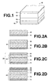
- FIG. 1 is a schematic perspective view of the image recording medium according to an embodiment of the present invention, illustrating the construction thereof.
- the image recording medium 10 is constituted by a layer composite layered in the order of: a recording side electrode layer 11 transparent to recording radiation (e.g., X-rays) to be described later; a recording photoconductive layer 12 that shows conductivity when exposed to the recording radiation transmitted through the recording side electrode layer 11; a charge transport layer 13 that acts as substantially an insulator against charges charged on the recording side electrode layer 11 (charges of latent image polarity, negative charges for example) and as substantially a conductor for the charges of the opposite polarity (charges of transport polarity, positive charges for example); a readout photoconductive layer 14 that shows conductivity when exposed to readout light to be described later; and a readout side electrode layer 15 transparent to the readout light.
- a recording side electrode layer 11 transparent to recording radiation (e.g., X-rays) to be described later
- a recording photoconductive layer 12 that shows
- the recording side electrode layer 11 may be made of any material as long as it is transparent to radiation.
- a transparent glass plate with conductive material applied uniformly thereon Nesa film or the like, or the like may be used as the recording side electrode layer 11.
- a photoconductive material consisting primarily of a-Se is used for either of the recording photoconductive layer 12 or the readout photoconductive layer 14, and a photoconductive material consisting primarily of sintered compacts of Bi-system compound is used for the other.
- the present embodiment will be described on the assumption that the recording photoconductive layer 12 consists primarily of sintered compacts of Bi 12 MO 20 , and the readout photoconductive layer 14 consists primarily of a-Se.
- a sintered film of polycrystalline substance made of Bi 12 MO 20 (M is at least one of Ge, Si or Ti) having a filling rate of not less than 70% with layer thickness from 50 ⁇ m to 600 ⁇ m as described in European patent Publication No. 1376245 , sintered compacts of Bi 2 O 3 as described in Japanese Patent Application No. 2004-109849 , sintered compacts of Bi 2 Ti 7 O 7 as described in Japanese Patent Application No. 2004-109850 , or sintered compacts of BiMO 4 (M is at least one of V, Nb or Ta) as described in Japanese Patent Application No. 2004-279708 may be used for the photoconductive layer.
- materials having a greater difference in charge mobility between the negative charges charged on the recording side electrode layer 11 and the opposite positive charges are preferable.
- These materials include organic compounds such as poly N-vinylcarbazole (PVK), N,N'-diphenyl-N,N'-bis(3-methylphenyl)-[1,1'-biphenyl]-4,4'-dia mine (TPD), discotic liquid crystal, and the like, or semiconductor materials such as TPD-dispersed polymers (polycarbonate, polystyrene, PUK), a-Se doped with 10 to 200 ppm of Cl, and the like.
- the organic compounds are preferable, since these materials are insensitive to light. Moreover, these materials have generally a small dielectric constant, resulting in small capacitance of the capacitor formed between the charge transport layer 13 and readout photoconductive layer 14, and thereby signal extraction efficiency may be improved when the signal charges are read out.
- the charge transport 13 may be a selenium arsenic alloy doped with halogen.
- the amount of the halogen is preferable to be in the range from 10 to 200 ppm in weight.
- the amount of halogen is not greater than 20 ppm in weight if the arsenic is not doped.
- the image recording medium 10 does not necessarily include the charge transport layer 13.
- the readout side electrode layer 15 maybe a transparent glass plate with a conductive material applied uniformly thereon (Nesa film or the like) like the recording side electrode layer 11. But it may be constituted by a comb electrode like that used in the image recording medium as described, for example, in U.S. Patent Application Publication No. 20040227114 .
- the recording side electrode layer 11 and recording photoconductive layer 12 consisting primarily of sintered compacts of Bi 12 MO 20 are formed ( Figure 2A).
- the charge transport layer 13 is further formed ( Figure 2B).
- the readout photoconductive layer 14 consisting primarily of a-Se is formed by deposition on the layer composite 21 that includes the recording photoconductive layer 12. More specifically, Se material is put on a vacuum deposition board (made of stainless steel or tungsten) which is then heated by the electric current flown through the board and thereby the Se material is heated and evaporated.
- the layer composite 21 is heated to a temperature in the range from 40 to 70 degrees Celsius, and evaporated Se particles adhere to the layer composite 21 to form an a-Se film on the layer composite 21.
- the layer composite 21 is heated to a temperature in the range from 40 to 70 degrees Celsius.
- the sintering temperature of the sintered compacts of Bi 12 MO 20 is approximately 800 degrees Celsius, so that substantially no damage is caused to the sintered compacts of Bi 12 MO 20 in the a-Se deposition process.
- the charge transport layer 13 is not provided between the recording photoconductive layer 12 and readout photoconductive layer 14, or another layer having a certain function is provided between the recording photoconductive layer 12 and readout photoconductive layer 14.
- the readout photoconductive layer 14 consisting primarily of a-Se is formed by deposition after the recording photoconductive layer 12 consisting primarily of sintered compacts of Bi 12 MO 20 is formed.
- the readout side electrode layer 15 is bonded to the layer composite 22 that includes the readout photoconductive layer 14 by the adhesive 23 ( Figure 2D).
- the adhesive 23 is omitted for clarity.
- the adhesive 23 is light curable and non-water soluble.
- the adhesive 23 may be conductive or nonconductive since it is applied thinly and uniformly to the readout side electrode layer 15.
- the readout photoconductive layer 14 consisting primarily of a-Se is formed by deposition after the recording photoconductive layer 12 consisting primarily of sintered compacts of Bi 12 MO 20 is formed.
- photoconductive layer 14 consisting primarily of a-Se to the layer composite 21 that includes the reading photoconductive layer 12 consisting primarily of sintered compacts of Bi 12 MO 20 by an anisotropic conductive adhesive is not required. Accordingly, no heating or pressurizing is required in the process of manufacturing the image recording medium 10 and thereby a-Se used is prevented from degradation or destruction. That is, the yield rate of the image recording medium 10 may be improved.
- FIG. 3 is a schematic configuration diagram of a recording/readout system 20 (combined system of an electrostatic latent image recording unit and an electrostatic latent image readout unit) that includes an image recording medium 10.
- the recording/readout system 20 is constituted by the image recording medium 10; a radiation irradiating section 90; a power source 50; a current detecting section 70; a readout exposure section 92; and switches S1 and S2.
- the image recording medium 10, power supply 50, radiation irradiating section 90, and the switch S1 constitute the section corresponding to the electrostatic latent image recording unit.
- the image recording medium 10, current detecting section 70, switch S2, and readout exposure section 92 constitute the section corresponding to the electrostatic latent image readout unit.
- the adhesive 23 shown in Figure 2D is omitted for clarity.
- the recording side electrode 11 of the image recording medium 10 is connected to the negative pole of the power source 10 through switch S1 and one end of the switch S2.
- the terminal 60 of the switch S2 is connected to the current detecting section 70.
- the terminal 62 of the switch S2 is connected to the readout side electrode layer 15 of the image recording medium 10, positive pole of the power supply 50, and ground.
- the current detecting section 70 includes a detecting amplifier 70a, which is an operational amplifier, and a feedback resister 70b, thereby forming a so-called a current/voltage conversion circuit.
- a subject 9 is positioned above the recording side electrode layer 11.
- the subject 9 includes a section 9a which is transparent to recording radiation L1 and a blocking section (light shielding section) 9b which is opaque to the recording radiation L1.
- the radiation irradiating section 90 is provided for irradiating the recording radiation L1 uniformly on the subject 9.
- the readout exposure section 92 is provided for scan exposing with readout light L2, such as an infrared laser beam, LED, or EL, in the direction indicated by the arrow in Figure 3.
- the readout light L2 is in the form of a beam focused into a small diameter.
- Figures 4A to 4D are drawings for explaining the recording process of an electrostatic latent image in the recording/readout system 20 using a charge model.
- Figure 5A to 5B are drawings for explaining the readout process of an electrostatic latent image in the recording/readout system 20 using a charge model.
- the switch S2 is switched open in which the switch S2 touches neither the terminal 61 nor terminal 62.
- the switch S1 is switched on to apply a DC voltage Ed supplied by the power supply 50 between the recording side electrode layer 11 and readout side electrode layer 15 such that negative charges are charged on the recording side electrode layer 11 and positive charges are charged on the readout side electrode layer 15 ( Figure 4A) .
- the recording radiation L1 is irradiated uniformly onto the subject 9 from the radiation irradiating section 90. Some of the recording radiation L1 transmits through the transparent section 9a of the subject 9 and further transmits through the recording side electrode layer 11.
- the recording photoconductive layer 12 shows conductivity when exposed to the recording radiation L1 transmitted through the recording side electrode layer 11. This process is like the operation of a variable resistor that varies its resistance value according to the radiation dose of the recording radiation L1. The resistance value depends on the amount of positive/negative charge pairs generated by the recording radiation L1, and if the radiation dose of the recording radiation L1 transmitted through the subject 9 is small, the variable resistor shows a high resistance value.
- the negative and positive charges generated by the recording radiation L1 are indicated by encircled minus (-) signs and encircled plus (+) signs respectively in the drawings.
- the positive charges generated in the recording photoconductive layer 12 move rapidly through the recording photoconductive layer 12 toward the recording side electrode layer 11, and disappear through charge recombination with the negative charges charged at the interface between the recording side electrode layer 11 and recording photoconductive layer 12( Figure 4C and 4D.
- the negative charges generated in the recording photoconductive layer 12 move through the recording photoconductive layer 12 toward the charge transport layer 13.
- the charge transport layer 13 acts as an insulator against the charges of the latent image polarity which is the same polarity of the charges charged on the recording side electrode layer 11 (negative charges in the present example).
- the negative charges moving through the recording photoconductive layer 12 are blocked at the charge storage section 31 formed at the interface between the recording photoconductive layer 12 and charge transport layer 13.
- the negative charges moving through the recording photoconductive layer 12 are stored in the charge storage section 31.
- the amount of charges stored in the charge storage section 31 depends on the amount of negative charges generated in the recording photoconductive layer 12 or the radiation dose of the recording radiation L1 transmitted through the subject 9.
- the charge storage section 31 is formed at the interface between the recording photoconductive layer 12 and charge transport layer 13. If the charge transport layer 13 is not included in the image recording medium 10, the charge storage section 31 is formed at the interface between the recording photoconductive layer 12 and readout photoconductive layer 14.
- the recording radiation L1 does not transmit through the light shielding section 9b of the subject 9, so that the portion of the image recording medium 10 that lies under the light shielding section 9b of the subject 9 shows no changes ( Figures 4B to 4D) .
- charges are stored in the charge storage section 31 according to the subject image.
- the electrostatic latent image readout process will be described with reference to Figures 5A to 5D.
- the voltage supply to the image recording medium 10 is terminated by switching off the switch S1.
- the rearrangement of charges is implemented by connecting the opposite end of the switch S2 to the terminal 62 and making the recording side electrode layer 11 and readout side electrode layer 15 at the same potential.
- the readout light L2 transmits through the readout side electrode layer 15, and the readout photoconductive layer 14 irradiated by the readout light L2 transmitted through the readout side electrode layer 15 shows conductivity.
- the positive/negative charge pairs are generated in the readout photoconductive layer 14 when exposed to the readout light L2, like the positive/negative charge pairs are generated in the recording photoconductive layer 12 when exposed to the recording radiation L1( Figure 5B).
- the negative and positive charges generated by the readout light L2 are indicated by encircled minus (-) signs and encircled plus (+) signs respectively in the drawings as in the recording process.
- a very strong electric field is formed between the charge storage section 31 storing the charges of latent image polarity and readout electrode layer 15 depending on the total film thickness of the readout photoconductive layer 14 and charge transport layer 13, and the amount of the charges of latent image polarity.
- the charge transport layer 13 acts as a conductor for positive charges
- the positive charges generated in the readout photoconductive layer 14 move rapidly through the charge transport layer 13 attracted by the negative charges stored in the charge storage section 31 and disappear through charge recombination with the negative charges at the charge storage section 31.
- negative charges generated in the readout photoconductive layer 14 are recombined with the positive charges of the readout side electrode layer 15 and disappear (Figure 5C).
- the readout photoconductive layer 14 is scan exposed with a sufficient amount of light by the readout light L2 to cause the negative charges stored in the charge storage section 31, i.e. electrostatic latent image to be disappeared through the charge recombination.
- Disappearance of the charges stored in the image recording medium 10 in the manner as described above means that a current I caused by the movement of the charges flows in the image recording medium 10. That is, the image recording medium 10 may be expressed by the equivalent circuit representing a current source that flows an amount of current according to the amount of charges stored therein like that shown in Figure 5D.
- the amount of charges of each of the sections corresponding to each of the pixels may be read out. That is, by scan exposing the entire region of the readout side electrode layer 15, the electrostatic latent image recorded in the image recording medium 10 may be read out.
Landscapes
- Measurement Of Radiation (AREA)
- Solid State Image Pick-Up Elements (AREA)
- Transforming Light Signals Into Electric Signals (AREA)
Abstract
A method for manufacturing an image recording medium constituted by a layer composite layered in the order of: a recording side electrode layer (11) transparent to recording radiation; a recording photoconductive layer (12) that shows photoconductivity when exposed to the recording radiation; a charge storage section (31) for storing charges of a latent image polarity generated in the recording photoconductive layer (12); a readout photoconductive layer (14) that shows photoconductivity when exposed to a readout electromagnetic wave; and a readout side electrode layer (15) transparent to the readout electromagnetic wave. In the layer composite, either of the recording photoconductive layer (12) or readout photoconductive layer (14) consists primarily of a-Se, and the other consists primarily of sintered compacts of Bi-system compound. The photoconductive layer consisting primarily of a-Se is formed by deposition after the photoconductive layer consisting primarily of sintered compacts of Bi-system compound is formed.
Description
- The present invention relates to a method for manufacturing an image recording medium capable of recording image information as an electrostatic latent image.
- In the medical radiation imaging, image recording media that include a radiation sensitive photoconductor are used abundantly for reducing the radiation dosage received by the subject and improving diagnostic performance. When radiation is irradiated on the image recording medium that includes the photoconductor, electric charges (latent image charges) are stored in the medium according to the dose of the radiation. Thereafter, the radiation image information may be read out from the image recording medium by detecting the charges stored in the medium.
- An image recording medium constituted by a layer composite is known as such image recording medium. The layer composite includes: a recording side electrode layer transparent to recording radiation; a recording photoconductive layer that shows photoconductivity when exposed to the recording radiation; a readout photoconductive layer that shows photoconductivity when exposed to a readout electromagnetic wave; a readout side electrode layer transparent to the readout electromagnetic wave. In such image recording medium, it is conceivable that a photoconductive material consisting primarily of a-Se is used, for example, for either of the readout photoconductive layer or recording photoconductive layer, and a photoconductive material consisting primarily of sintered compacts of Bi12MO20 (M is one of Ge, Si or Ti) is used for the other.
- A method for manufacturing an image recording medium by bonding an active matrix substrate having an electric charge storing capacitor and a TFT (thin film transistor) to an opposing substrate having photoconductivity (compound semiconductor such as CdTe, CdZnTe or the like) using an anisotropic conductive adhesive is disclosed in
U.S. patent No. 6,262,408 as a method for manufacturing an image recording medium by bonding different kinds of materials together. - Thus, in manufacturing an image recording medium that includes a photoconductive layer consisting primarily of a-Se, and a photoconductive layer consisting primarily of sintered compacts of Bi12MO20, it is conceivable that the image recording medium may be manufactured by bonding a single readout photoconductive layer or a layer composite including the readout photoconductive layer to a single recording photoconductive layer or a layer composite including the recording photoconductive layer using an anisotropic conductive adhesive.
- The use of anisotropic conductive adhesive for bonding, however, requires heating, pressurizing, or the like in order to force the diameter of the conductive particles included in the adhesive to conform to the application thickness of the adhesive when performing the bonding. But a-Se is prone to degradation or destruction by heat or high pressure, and is degraded or destroyed by the heat or pressure applied thereto when the bonding is performed. Thus, the method using the anisotropic conductive adhesive is not suited for manufacturing an image recording medium having a photoconductive layer that includes a-Se.
- The present invention has been developed in view of the circumstances described above, and it is an object of the present invention to provide a method for manufacturing an image recording medium that includes a photoconductive layer consisting primarily of a-Se, in which the a-Se may be prevented from degradation or destruction.
- The method for manufacturing an image recording medium of the present invention is a method for manufacturing an image recording medium constituted by a layer composite layered in the order of:
- a recording side electrode layer transparent to recording radiation;
- a recording photoconductive layer that shows photoconductivity when exposed to the recording radiation;
- a charge storage section for storing charges of latent image polarity generated in the recording photoconductive layer;
- a readout photoconductive layer that shows photoconductivity when exposed to a readout electromagnetic wave; and
- a readout side electrode layer transparent to the readout electromagnetic wave, wherein:
- either of the recording photoconductive layer or readout photoconductive layer consists primarily of a-Se, and the other consists primarily of sintered compacts of Bi-system compound; and
- the photoconductive layer consisting primarily of a-Se is formed by deposition after the photoconductive layer consisting primarily of sintered compacts of Bi-system compound is formed.
- The referent of "consists primarily of a-Se" as used herein means that a-Se is included more than or equal to 90% as the major component of the photoconductive layer. Likewise, the referent of "consists primarily of sintered compacts of Bi-system compound" as used herein means that sintered compacts of Bi-system compound is included more than or equal to 90% as the major component of the photoconductive layer.
- Further, the referent of "the photoconductive layer consisting primarily of a-Se is formed by deposition after the photoconductive layer consisting primarily of sintered compacts of Bi-system compound is formed" as used herein means that the photoconductive layer consisting primarily of a-Se is formed by depositing the layer on a single layer consisting primarily of sintered compacts of Bi-system compound or on a layer composite that includes the layer consisting primarily of sintered compacts of Bi-system compound.
- The recording photoconductive layer may consist primarily of sintered compacts of Bi-system compound, and the readout photoconductive layer may consist primarily of a-Se. Further, the sintered compacts of Bi-system may be sintered compacts of Bi12MO20 (M is one of Ge, Si or Ti) . Still further, the readout photoconductive layer and readout side electrode layer may be bonded together by an adhesive. Preferably, the adhesive is a light curable adhesive.
- According to the method for manufacturing an image recording medium of the present invention, the photoconductive layer consisting primarily of a-Se is formed by deposition after the photoconductive layer consisting primarily of sintered compacts of Bi-system compound is formed. This method does not require bonding of the substrate that includes the photoconductive layer consisting primarily of a-Se and the substrate that includes the photoconductive layer consisting primarily of sintered compacts of Bi-system compound together using an anisotropic conductive adhesive. Accordingly, no heating or pressurizing is required in the process of manufacturing an image recording medium and thereby a-Se used is prevented from degradation or destruction. That is, the yield rate of the image recording medium may be improved.
-
- Figure 1 is a schematic perspective view of the image recording medium according to an embodiment of the present invention, illustrating the construction thereof.
- Figures 2A to 2D are drawings for explaining the method for manufacturing the image recording medium according to an embodiment.
- Figure 3 is a schematic configuration diagram of a recording/readout system that includes the image recording medium.
- Figures 4A to 4D are drawings for explaining the process of recording an electrostatic latent image in the recording/readout system using a charge model.
- Figures 5A to 5D are drawings for explaining the process of reading out the electrostatic latent image in the recording/readout system using a charge model.
- The construction of the image recording medium of the present invention will be described first with reference to Figure 1. Figure 1 is a schematic perspective view of the image recording medium according to an embodiment of the present invention, illustrating the construction thereof. The
image recording medium 10 is constituted by a layer composite layered in the order of: a recordingside electrode layer 11 transparent to recording radiation (e.g., X-rays) to be described later; a recordingphotoconductive layer 12 that shows conductivity when exposed to the recording radiation transmitted through the recordingside electrode layer 11; acharge transport layer 13 that acts as substantially an insulator against charges charged on the recording side electrode layer 11 (charges of latent image polarity, negative charges for example) and as substantially a conductor for the charges of the opposite polarity (charges of transport polarity, positive charges for example); a readoutphotoconductive layer 14 that shows conductivity when exposed to readout light to be described later; and a readoutside electrode layer 15 transparent to the readout light. - The recording
side electrode layer 11 may be made of any material as long as it is transparent to radiation. For example, a transparent glass plate with conductive material applied uniformly thereon (Nesa film or the like), or the like may be used as the recordingside electrode layer 11. - A photoconductive material consisting primarily of a-Se is used for either of the recording
photoconductive layer 12 or the readoutphotoconductive layer 14, and a photoconductive material consisting primarily of sintered compacts of Bi-system compound is used for the other. The present embodiment will be described on the assumption that the recordingphotoconductive layer 12 consists primarily of sintered compacts of Bi12MO20, and the readoutphotoconductive layer 14 consists primarily of a-Se. Further, instead of the sintered compacts of Bi12MO20 described above, sintered compacts of Bi12M3O12, a sintered film of polycrystalline substance made of Bi12MO20 (M is at least one of Ge, Si or Ti) having a filling rate of not less than 70% with layer thickness from 50µm to 600µm as described inEuropean patent Publication No. 1376245 , sintered compacts of Bi2O3 as described inJapanese Patent Application No. 2004-109849 Japanese Patent Application No. 2004-109850 Japanese Patent Application No. 2004-279708 - As for the material of the
charge transport layer 13, materials having a greater difference in charge mobility between the negative charges charged on the recordingside electrode layer 11 and the opposite positive charges are preferable. These materials include organic compounds such as poly N-vinylcarbazole (PVK), N,N'-diphenyl-N,N'-bis(3-methylphenyl)-[1,1'-biphenyl]-4,4'-dia mine (TPD), discotic liquid crystal, and the like, or semiconductor materials such as TPD-dispersed polymers (polycarbonate, polystyrene, PUK), a-Se doped with 10 to 200 ppm of Cl, and the like. In particular, the organic compounds (PVK, TPD, discotic liquid crystal, and the like) are preferable, since these materials are insensitive to light. Moreover, these materials have generally a small dielectric constant, resulting in small capacitance of the capacitor formed between thecharge transport layer 13 and readoutphotoconductive layer 14, and thereby signal extraction efficiency may be improved when the signal charges are read out. Further, thecharge transport 13 may be a selenium arsenic alloy doped with halogen. Here, the amount of the halogen is preferable to be in the range from 10 to 200 ppm in weight. Preferably, the amount of halogen is not greater than 20 ppm in weight if the arsenic is not doped. Incidentally, theimage recording medium 10 does not necessarily include thecharge transport layer 13. - The readout
side electrode layer 15 maybe a transparent glass plate with a conductive material applied uniformly thereon (Nesa film or the like) like the recordingside electrode layer 11. But it may be constituted by a comb electrode like that used in the image recording medium as described, for example, inU.S. Patent Application Publication No. 20040227114 . - Hereinafter, a method for manufacturing the
image recording medium 10 will be specifically described with reference to Figures 2A to 2D. First, the recordingside electrode layer 11 and recordingphotoconductive layer 12 consisting primarily of sintered compacts of Bi12MO20 are formed (Figure 2A). When thecharge transport layer 13 is to be included in theimage recording medium 10, thecharge transport layer 13 is further formed (Figure 2B). Thereafter, the readoutphotoconductive layer 14 consisting primarily of a-Se is formed by deposition on thelayer composite 21 that includes the recordingphotoconductive layer 12. More specifically, Se material is put on a vacuum deposition board (made of stainless steel or tungsten) which is then heated by the electric current flown through the board and thereby the Se material is heated and evaporated. Thelayer composite 21 is heated to a temperature in the range from 40 to 70 degrees Celsius, and evaporated Se particles adhere to thelayer composite 21 to form an a-Se film on thelayer composite 21. When the Se material is deposited, thelayer composite 21 is heated to a temperature in the range from 40 to 70 degrees Celsius. But the sintering temperature of the sintered compacts of Bi12MO20 is approximately 800 degrees Celsius, so that substantially no damage is caused to the sintered compacts of Bi12MO20 in the a-Se deposition process. There may be a case where thecharge transport layer 13 is not provided between therecording photoconductive layer 12 andreadout photoconductive layer 14, or another layer having a certain function is provided between therecording photoconductive layer 12 andreadout photoconductive layer 14. In any case, thereadout photoconductive layer 14 consisting primarily of a-Se is formed by deposition after therecording photoconductive layer 12 consisting primarily of sintered compacts of Bi12MO20 is formed. - Then, the readout
side electrode layer 15 is bonded to thelayer composite 22 that includes thereadout photoconductive layer 14 by the adhesive 23 (Figure 2D). In theimage recording medium 10 shown in Figure 1, the adhesive 23 is omitted for clarity. Preferably, the adhesive 23 is light curable and non-water soluble. Further, the adhesive 23 may be conductive or nonconductive since it is applied thinly and uniformly to the readoutside electrode layer 15. - As described above, the
readout photoconductive layer 14 consisting primarily of a-Se is formed by deposition after therecording photoconductive layer 12 consisting primarily of sintered compacts of Bi12MO20 is formed. Thus, bonding of the readout.photoconductive layer 14 consisting primarily of a-Se to thelayer composite 21 that includes the readingphotoconductive layer 12 consisting primarily of sintered compacts of Bi12MO20 by an anisotropic conductive adhesive is not required. Accordingly, no heating or pressurizing is required in the process of manufacturing theimage recording medium 10 and thereby a-Se used is prevented from degradation or destruction. That is, the yield rate of theimage recording medium 10 may be improved. - Hereinafter, the method for recording an electrostatic latent image on the image recording medium, and the method for reading out the electrostatic latent image from the medium will be described. The referent of "electrostatic latent image" as used herein means a subject image represented by the charges stored in the image recording medium. Figure 3 is a schematic configuration diagram of a recording/readout system 20 (combined system of an electrostatic latent image recording unit and an electrostatic latent image readout unit) that includes an
image recording medium 10. The recording/readout system 20 is constituted by theimage recording medium 10; aradiation irradiating section 90; apower source 50; a current detectingsection 70; areadout exposure section 92; and switches S1 and S2. Of these, theimage recording medium 10,power supply 50,radiation irradiating section 90, and the switch S1 constitute the section corresponding to the electrostatic latent image recording unit. Theimage recording medium 10, current detectingsection 70, switch S2, andreadout exposure section 92 constitute the section corresponding to the electrostatic latent image readout unit. In theimage recording medium 10 shown in Figures 3 to 5, the adhesive 23 shown in Figure 2D is omitted for clarity. - The
recording side electrode 11 of theimage recording medium 10 is connected to the negative pole of thepower source 10 through switch S1 and one end of the switch S2. The terminal 60 of the switch S2 is connected to the current detectingsection 70. The terminal 62 of the switch S2 is connected to the readoutside electrode layer 15 of theimage recording medium 10, positive pole of thepower supply 50, and ground. The current detectingsection 70 includes a detectingamplifier 70a, which is an operational amplifier, and afeedback resister 70b, thereby forming a so-called a current/voltage conversion circuit. - A subject 9 is positioned above the recording
side electrode layer 11. Thesubject 9 includes asection 9a which is transparent to recording radiation L1 and a blocking section (light shielding section) 9b which is opaque to the recording radiation L1. Theradiation irradiating section 90 is provided for irradiating the recording radiation L1 uniformly on thesubject 9. Thereadout exposure section 92 is provided for scan exposing with readout light L2, such as an infrared laser beam, LED, or EL, in the direction indicated by the arrow in Figure 3. Preferably, the readout light L2 is in the form of a beam focused into a small diameter. - Figures 4A to 4D are drawings for explaining the recording process of an electrostatic latent image in the recording/
readout system 20 using a charge model. Figure 5A to 5B are drawings for explaining the readout process of an electrostatic latent image in the recording/readout system 20 using a charge model. Initially, the switch S2 is switched open in which the switch S2 touches neither the terminal 61 norterminal 62. Then, the switch S1 is switched on to apply a DC voltage Ed supplied by thepower supply 50 between the recordingside electrode layer 11 and readoutside electrode layer 15 such that negative charges are charged on the recordingside electrode layer 11 and positive charges are charged on the readout side electrode layer 15 (Figure 4A) . This creates a parallel electric field in theimage recording medium 10 between the recordingside electrode layer 11 and readoutside electrode layer 15. - Then, the recording radiation L1 is irradiated uniformly onto the subject 9 from the
radiation irradiating section 90. Some of the recording radiation L1 transmits through thetransparent section 9a of the subject 9 and further transmits through the recordingside electrode layer 11. Therecording photoconductive layer 12 shows conductivity when exposed to the recording radiation L1 transmitted through the recordingside electrode layer 11. This process is like the operation of a variable resistor that varies its resistance value according to the radiation dose of the recording radiation L1. The resistance value depends on the amount of positive/negative charge pairs generated by the recording radiation L1, and if the radiation dose of the recording radiation L1 transmitted through thesubject 9 is small, the variable resistor shows a high resistance value. The negative and positive charges generated by the recording radiation L1 are indicated by encircled minus (-) signs and encircled plus (+) signs respectively in the drawings. - The positive charges generated in the
recording photoconductive layer 12 move rapidly through therecording photoconductive layer 12 toward the recordingside electrode layer 11, and disappear through charge recombination with the negative charges charged at the interface between the recordingside electrode layer 11 and recording photoconductive layer 12(Figure 4C and 4D. In the mean time, the negative charges generated in therecording photoconductive layer 12 move through therecording photoconductive layer 12 toward thecharge transport layer 13. Thecharge transport layer 13 acts as an insulator against the charges of the latent image polarity which is the same polarity of the charges charged on the recording side electrode layer 11 (negative charges in the present example). Thus, the negative charges moving through therecording photoconductive layer 12 are blocked at thecharge storage section 31 formed at the interface between therecording photoconductive layer 12 andcharge transport layer 13. That is, the negative charges moving through therecording photoconductive layer 12 are stored in thecharge storage section 31. The amount of charges stored in thecharge storage section 31 depends on the amount of negative charges generated in therecording photoconductive layer 12 or the radiation dose of the recording radiation L1 transmitted through thesubject 9. - Here, the description has been made that the
charge storage section 31 is formed at the interface between therecording photoconductive layer 12 andcharge transport layer 13. If thecharge transport layer 13 is not included in theimage recording medium 10, thecharge storage section 31 is formed at the interface between therecording photoconductive layer 12 andreadout photoconductive layer 14. - In the mean time, the recording radiation L1 does not transmit through the
light shielding section 9b of the subject 9, so that the portion of theimage recording medium 10 that lies under thelight shielding section 9b of the subject 9 shows no changes (Figures 4B to 4D) . As described above, by irradiating the reading radiation L1 on thesubject 9, charges are stored in thecharge storage section 31 according to the subject image. - Hereinafter, the electrostatic latent image readout process will be described with reference to Figures 5A to 5D. Initially, the voltage supply to the
image recording medium 10 is terminated by switching off the switch S1. Then, the rearrangement of charges is implemented by connecting the opposite end of the switch S2 to the terminal 62 and making the recordingside electrode layer 11 and readoutside electrode layer 15 at the same potential. - When the readout
side electrode layer 15 is scan exposed with the readout light L2 by thereadout exposure section 92, the readout light L2 transmits through the readoutside electrode layer 15, and thereadout photoconductive layer 14 irradiated by the readout light L2 transmitted through the readoutside electrode layer 15 shows conductivity. This is due to the fact that the positive/negative charge pairs are generated in thereadout photoconductive layer 14 when exposed to the readout light L2, like the positive/negative charge pairs are generated in therecording photoconductive layer 12 when exposed to the recording radiation L1(Figure 5B). The negative and positive charges generated by the readout light L2 are indicated by encircled minus (-) signs and encircled plus (+) signs respectively in the drawings as in the recording process. - A very strong electric field (intense electric field) is formed between the
charge storage section 31 storing the charges of latent image polarity andreadout electrode layer 15 depending on the total film thickness of thereadout photoconductive layer 14 andcharge transport layer 13, and the amount of the charges of latent image polarity. Here, since thecharge transport layer 13 acts as a conductor for positive charges, the positive charges generated in thereadout photoconductive layer 14 move rapidly through thecharge transport layer 13 attracted by the negative charges stored in thecharge storage section 31 and disappear through charge recombination with the negative charges at thecharge storage section 31. In the mean time, negative charges generated in thereadout photoconductive layer 14 are recombined with the positive charges of the readoutside electrode layer 15 and disappear (Figure 5C). Thereadout photoconductive layer 14 is scan exposed with a sufficient amount of light by the readout light L2 to cause the negative charges stored in thecharge storage section 31, i.e. electrostatic latent image to be disappeared through the charge recombination. Disappearance of the charges stored in theimage recording medium 10 in the manner as described above means that a current I caused by the movement of the charges flows in theimage recording medium 10. That is, theimage recording medium 10 may be expressed by the equivalent circuit representing a current source that flows an amount of current according to the amount of charges stored therein like that shown in Figure 5D. - By scan exposing each of the sections corresponding to each of the pixels on the
image recording medium 10 by the readout light L2 in the manner as described above, the amount of charges of each of the sections corresponding to each of the pixels may be read out. That is, by scan exposing the entire region of the readoutside electrode layer 15, the electrostatic latent image recorded in theimage recording medium 10 may be read out. - The
image recording medium 10 according to the present embodiment includes therecording photoconductive layer 12 andcharge transport layer 13 with thecharge storage section 31 being formed at the interface between therecording photoconductive layer 12 andcharge transport layer 13. But thecharge transport layer 13 may be replaced by a trap layer, in which case the latent image charges are captured by the trap layer, and stored in the trap layer or at the interface between the trap layer andrecording photoconductive layer 12.
Claims (5)
- A method for manufacturing an image recording medium constituted by a layer composite layered in the order of:a recording side electrode layer (11) transparent to recording radiation;a recording photoconductive layer (12) that shows photoconductivity when exposed to the recording radiation;a charge storage section (31) for storing charges of latent image polarity generated in the recording photoconductive layer (12);a readout photoconductive layer (14) that shows photoconductivity when exposed to a readout electromagnetic wave; anda readout side electrode layer (15) transparent to the readout electromagnetic wave, wherein:either of the recording photoconductive layer (12) or readout photoconductive layer (14) consists primarily of a-Se, and the other consists primarily of sintered compacts of Bi-system compound; andthe photoconductive layer consisting primarily of a-Se is formed by deposition after the photoconductive layer consisting primarily of sintered compacts of Bi-system compound is formed.
- The method for manufacturing an image recording medium according to claim 1, wherein the recording photoconductive layer (12) consists primarily of sintered compacts of Bi-system compound, and the readout photoconductive layer (14) consists primarily of a-Se.
- The method for manufacturing an image recording medium according to claim 1 or 2, wherein the sintered compacts of Bi-system compound are sintered compacts of Bi12MO20 (M is one of Ge, Si or Ti).
- The method for manufacturing an image recording medium according to claim 2 or 3, wherein the readout photoconductive layer (14) and readout side electrode layer (15) are bonded together by an adhesive (23).
- The method for manufacturing an image recording medium according to claim 4, wherein the adhesive (23) is a light curable adhesive.
Applications Claiming Priority (1)
| Application Number | Priority Date | Filing Date | Title |
|---|---|---|---|
| JP2005081066A JP2006269465A (en) | 2005-03-22 | 2005-03-22 | Manufacturing method of image recording medium |
Publications (1)
| Publication Number | Publication Date |
|---|---|
| EP1705707A2 true EP1705707A2 (en) | 2006-09-27 |
Family
ID=36607586
Family Applications (1)
| Application Number | Title | Priority Date | Filing Date |
|---|---|---|---|
| EP06005870A Withdrawn EP1705707A2 (en) | 2005-03-22 | 2006-03-22 | Method for manufacturing image recording medium |
Country Status (3)
| Country | Link |
|---|---|
| US (1) | US20060226382A1 (en) |
| EP (1) | EP1705707A2 (en) |
| JP (1) | JP2006269465A (en) |
Family Cites Families (2)
| Publication number | Priority date | Publication date | Assignee | Title |
|---|---|---|---|---|
| JP3649907B2 (en) * | 1998-01-20 | 2005-05-18 | シャープ株式会社 | Two-dimensional image detector and manufacturing method thereof |
| JP2004342691A (en) * | 2003-05-13 | 2004-12-02 | Fuji Photo Film Co Ltd | Radiation image detector |
-
2005
- 2005-03-22 JP JP2005081066A patent/JP2006269465A/en not_active Withdrawn
-
2006
- 2006-03-22 US US11/385,852 patent/US20060226382A1/en not_active Abandoned
- 2006-03-22 EP EP06005870A patent/EP1705707A2/en not_active Withdrawn
Also Published As
| Publication number | Publication date |
|---|---|
| JP2006269465A (en) | 2006-10-05 |
| US20060226382A1 (en) | 2006-10-12 |
Similar Documents
| Publication | Publication Date | Title |
|---|---|---|
| US7709804B2 (en) | Radiation detector | |
| JPH03185865A (en) | Solid-state radiation sensor array panel | |
| EP1978563A2 (en) | Radiation detector and method for producing photoconductive layer for recording thereof | |
| US7786446B2 (en) | Radiation detector | |
| Street et al. | X-ray imaging using lead iodide as a semiconductor detector | |
| JP2009088154A (en) | Radiation detector | |
| JP2011146541A (en) | X-ray detector and method of manufacturing the same | |
| US7723692B2 (en) | Solid state radiation sensor and manufacturing method of the same | |
| CA2336333A1 (en) | Direct radiographic imaging panel having a dielectric layer with an adjusted time constant | |
| EP1705707A2 (en) | Method for manufacturing image recording medium | |
| US8581198B2 (en) | Apparatus and method for detecting radiation | |
| US8415634B2 (en) | Apparatus and method for detecting radiation | |
| EP1262797B1 (en) | Method and apparatus for image recording and image recording medium | |
| JP2010027834A (en) | Method for manufacturing photoconductive layer for recording of radiation detector | |
| JP2000346951A (en) | Radiation solid detector, radiation image-recording/ reading method and device using the same | |
| JP4787227B2 (en) | Radiation detector and method for producing photoconductive layer for recording radiation detector | |
| JP4602205B2 (en) | Bi12MO20 precursor, manufacturing method of Bi12MO20 powder, and manufacturing method of photoconductive layer constituting radiation imaging panel | |
| JP2013545965A (en) | Radiation detector and radiation detection method | |
| JP2007005625A (en) | Photoconduction layer which constitutes radiation image pick-up panel and radiation image pickup panel | |
| US7429296B2 (en) | Method for manufacturing photoconductive layer constituting radiation imaging panel | |
| JP2007012843A (en) | Optical conductive layer and radiation imaging panel | |
| JP3999470B2 (en) | Radiation solid state detector, and radiation image recording / reading method and apparatus using the same | |
| EP1342105A2 (en) | Direct radiographic imaging panel with an imaging property reversibly adjustable with an external energy source in clinical use of the panel | |
| JP2007012841A (en) | Method of manufacturing optical conductive layer | |
| JP2006240953A (en) | Bi12TiO20 SINTERED COMPACT AND PHOTOCONDUCTIVE LAYER |
Legal Events
| Date | Code | Title | Description |
|---|---|---|---|
| PUAI | Public reference made under article 153(3) epc to a published international application that has entered the european phase |
Free format text: ORIGINAL CODE: 0009012 |
|
| AK | Designated contracting states |
Kind code of ref document: A2 Designated state(s): AT BE BG CH CY CZ DE DK EE ES FI FR GB GR HU IE IS IT LI LT LU LV MC NL PL PT RO SE SI SK TR |
|
| AX | Request for extension of the european patent |
Extension state: AL BA HR MK YU |
|
| RAP1 | Party data changed (applicant data changed or rights of an application transferred) |
Owner name: FUJIFILM CORPORATION |
|
| STAA | Information on the status of an ep patent application or granted ep patent |
Free format text: STATUS: THE APPLICATION IS DEEMED TO BE WITHDRAWN |
|
| 18D | Application deemed to be withdrawn |
Effective date: 20091001 |