EP1701393A1 - Organic thin film transistor and method of manufacturing thereof - Google Patents
Organic thin film transistor and method of manufacturing thereof Download PDFInfo
- Publication number
- EP1701393A1 EP1701393A1 EP06110603A EP06110603A EP1701393A1 EP 1701393 A1 EP1701393 A1 EP 1701393A1 EP 06110603 A EP06110603 A EP 06110603A EP 06110603 A EP06110603 A EP 06110603A EP 1701393 A1 EP1701393 A1 EP 1701393A1
- Authority
- EP
- European Patent Office
- Prior art keywords
- derivatives
- insulating film
- concave portions
- active layer
- organic
- Prior art date
- Legal status (The legal status is an assumption and is not a legal conclusion. Google has not performed a legal analysis and makes no representation as to the accuracy of the status listed.)
- Granted
Links
Images




Classifications
-
- H—ELECTRICITY
- H10—SEMICONDUCTOR DEVICES; ELECTRIC SOLID-STATE DEVICES NOT OTHERWISE PROVIDED FOR
- H10K—ORGANIC ELECTRIC SOLID-STATE DEVICES
- H10K71/00—Manufacture or treatment specially adapted for the organic devices covered by this subclass
- H10K71/60—Forming conductive regions or layers, e.g. electrodes
-
- H—ELECTRICITY
- H10—SEMICONDUCTOR DEVICES; ELECTRIC SOLID-STATE DEVICES NOT OTHERWISE PROVIDED FOR
- H10K—ORGANIC ELECTRIC SOLID-STATE DEVICES
- H10K10/00—Organic devices specially adapted for rectifying, amplifying, oscillating or switching; Organic capacitors or resistors having potential barriers
- H10K10/40—Organic transistors
- H10K10/46—Field-effect transistors, e.g. organic thin-film transistors [OTFT]
- H10K10/462—Insulated gate field-effect transistors [IGFETs]
- H10K10/468—Insulated gate field-effect transistors [IGFETs] characterised by the gate dielectrics
-
- H—ELECTRICITY
- H10—SEMICONDUCTOR DEVICES; ELECTRIC SOLID-STATE DEVICES NOT OTHERWISE PROVIDED FOR
- H10K—ORGANIC ELECTRIC SOLID-STATE DEVICES
- H10K10/00—Organic devices specially adapted for rectifying, amplifying, oscillating or switching; Organic capacitors or resistors having potential barriers
- H10K10/80—Constructional details
- H10K10/82—Electrodes
- H10K10/84—Ohmic electrodes, e.g. source or drain electrodes
-
- H—ELECTRICITY
- H10—SEMICONDUCTOR DEVICES; ELECTRIC SOLID-STATE DEVICES NOT OTHERWISE PROVIDED FOR
- H10K—ORGANIC ELECTRIC SOLID-STATE DEVICES
- H10K10/00—Organic devices specially adapted for rectifying, amplifying, oscillating or switching; Organic capacitors or resistors having potential barriers
- H10K10/40—Organic transistors
- H10K10/46—Field-effect transistors, e.g. organic thin-film transistors [OTFT]
- H10K10/462—Insulated gate field-effect transistors [IGFETs]
- H10K10/466—Lateral bottom-gate IGFETs comprising only a single gate
-
- H—ELECTRICITY
- H10—SEMICONDUCTOR DEVICES; ELECTRIC SOLID-STATE DEVICES NOT OTHERWISE PROVIDED FOR
- H10K—ORGANIC ELECTRIC SOLID-STATE DEVICES
- H10K59/00—Integrated devices, or assemblies of multiple devices, comprising at least one organic light-emitting element covered by group H10K50/00
- H10K59/10—OLED displays
- H10K59/12—Active-matrix OLED [AMOLED] displays
-
- H—ELECTRICITY
- H10—SEMICONDUCTOR DEVICES; ELECTRIC SOLID-STATE DEVICES NOT OTHERWISE PROVIDED FOR
- H10K—ORGANIC ELECTRIC SOLID-STATE DEVICES
- H10K77/00—Constructional details of devices covered by this subclass and not covered by groups H10K10/80, H10K30/80, H10K50/80 or H10K59/80
- H10K77/10—Substrates, e.g. flexible substrates
- H10K77/111—Flexible substrates
-
- H—ELECTRICITY
- H10—SEMICONDUCTOR DEVICES; ELECTRIC SOLID-STATE DEVICES NOT OTHERWISE PROVIDED FOR
- H10K—ORGANIC ELECTRIC SOLID-STATE DEVICES
- H10K85/00—Organic materials used in the body or electrodes of devices covered by this subclass
- H10K85/10—Organic polymers or oligomers
- H10K85/111—Organic polymers or oligomers comprising aromatic, heteroaromatic, or aryl chains, e.g. polyaniline, polyphenylene or polyphenylene vinylene
- H10K85/113—Heteroaromatic compounds comprising sulfur or selene, e.g. polythiophene
-
- H—ELECTRICITY
- H10—SEMICONDUCTOR DEVICES; ELECTRIC SOLID-STATE DEVICES NOT OTHERWISE PROVIDED FOR
- H10K—ORGANIC ELECTRIC SOLID-STATE DEVICES
- H10K85/00—Organic materials used in the body or electrodes of devices covered by this subclass
- H10K85/10—Organic polymers or oligomers
- H10K85/111—Organic polymers or oligomers comprising aromatic, heteroaromatic, or aryl chains, e.g. polyaniline, polyphenylene or polyphenylene vinylene
- H10K85/113—Heteroaromatic compounds comprising sulfur or selene, e.g. polythiophene
- H10K85/1135—Polyethylene dioxythiophene [PEDOT]; Derivatives thereof
-
- H—ELECTRICITY
- H10—SEMICONDUCTOR DEVICES; ELECTRIC SOLID-STATE DEVICES NOT OTHERWISE PROVIDED FOR
- H10K—ORGANIC ELECTRIC SOLID-STATE DEVICES
- H10K85/00—Organic materials used in the body or electrodes of devices covered by this subclass
- H10K85/10—Organic polymers or oligomers
- H10K85/111—Organic polymers or oligomers comprising aromatic, heteroaromatic, or aryl chains, e.g. polyaniline, polyphenylene or polyphenylene vinylene
- H10K85/114—Poly-phenylenevinylene; Derivatives thereof
-
- H—ELECTRICITY
- H10—SEMICONDUCTOR DEVICES; ELECTRIC SOLID-STATE DEVICES NOT OTHERWISE PROVIDED FOR
- H10K—ORGANIC ELECTRIC SOLID-STATE DEVICES
- H10K85/00—Organic materials used in the body or electrodes of devices covered by this subclass
- H10K85/60—Organic compounds having low molecular weight
- H10K85/615—Polycyclic condensed aromatic hydrocarbons, e.g. anthracene
-
- H—ELECTRICITY
- H10—SEMICONDUCTOR DEVICES; ELECTRIC SOLID-STATE DEVICES NOT OTHERWISE PROVIDED FOR
- H10K—ORGANIC ELECTRIC SOLID-STATE DEVICES
- H10K85/00—Organic materials used in the body or electrodes of devices covered by this subclass
- H10K85/60—Organic compounds having low molecular weight
- H10K85/615—Polycyclic condensed aromatic hydrocarbons, e.g. anthracene
- H10K85/621—Aromatic anhydride or imide compounds, e.g. perylene tetra-carboxylic dianhydride or perylene tetracarboxylic di-imide
Definitions
- the present invention relates to a thin film transistor, and more particularly to a method of manufacturing a thin film transistor using an organic semiconductor material as an active layer, a thin film transistor manufactured by the method, and a display device employing the same.
- a display device such as an organic light emitting display and a liquid crystal display which are small in thickness and operate with low voltages, unlike a cathode ray tube (CRT) which is bulky and operates with high voltages, is being widely used as the next generation display device.
- CTR cathode ray tube
- the organic light emitting display is a self-emitting display device in which electrons and holes injected into organic material through an anode and a cathode are recombined to generate excitons and light with a certain wavelength is emitted by energy of the generated excitons. Accordingly, the organic light emitting display is being highlighted as the next generation display device since it does not require a separate light source such as a backlight, and thus is low in its power consumption, as compared to the liquid crystal display, and in addition, may secure a wide viewing angle and a high response speed easily.
- the organic light emitting display which may be divided into a passive matrix type and an active matrix type depending on a driving method, has mainly employed the active matrix type in recent years owing to its low power consumption, high precision, high response speed, wide viewing angle and small thickness.
- pixels as the basic unit for image representation are arranged in the form of a matrix, and a thin film transistor (TFT) is arranged as a switching element for each of the pixels to be controlled separately.
- TFT thin film transistor
- organic TFT organic TFT
- organic semiconductor material instead of a typical TFT using silicon as an active layer, because the organic semiconductor material allows a low-temperature process and secures flexibility.
- the OTFT has a structure where a gate electrode and an active layer made of organic semiconductor material are formed on a substrate, with a gate insulating film disposed therebetween, and a source electrode and a drain electrode contact the active layer and are isolated from each other in correspondence to either side of the gate electrode.
- the OTFT may be divided into a low molecule OTFT made of such materials as pentacene and a high molecule OTFT made of such as polythiophene depending on the organic semiconductor material composing the active layer.
- the organic semiconductor material such as pentacene and polythiophene is difficult and complicated to be patterned since it has poor chemical and optical stability.
- organic semiconductor material has difficulty in securing good pattern precision, leading to high possibility of occurrence of particles, which may result in cross-talk with adjacent OTFTs.
- the present invention has been made to overcome the above and other problems, and it is an object of the present invention to provide a method of manufacturing a TFT, which is capable of enhancing pattern precision of an organic semiconductor material and simplifying a patterning process.
- a method of manufacturing a thin film transistor includes forming an organic insulating film on a substrate, forming a bank having first, second and third concave portions in the organic insulating film, the third concave portion being formed on the first and second concave portions, forming a source electrode and a drain electrode in the first and second concave portions, and forming an active layer in the third concave portion, the active layer contacting the source electrode and the drain electrode.
- the bank is formed by exposing the organic insulating film using a half tone mask and developing the exposed organic insulating film.
- the organic insulating film is made of a negative type photoresist or a positive type photoresist.
- the source electrode and the drain electrode are formed by dropping source and drain electrode material in the first and second concave portions using an ink-jet method and curing the substrate on which the source and drain electrode material is dropped.
- the source and drain electrode material includes at least one selected from the group including polyethylene dioxythiophene (PEDOT), polyaniline (PANI), conductive high molecules, Ag nano composite, Cu nano composite, Au nano composite, and Pt nano composite, or includes material formed by pattern-coating and firing material containing metal nano particles or carbon nano particles and organic binders, the metal nano particles or the carbon nano particles having a work function value larger than a value resulting from a subtraction of 0.5 eV from a HOMO (Highest Occupied Molecular Orbital) value of material composing the active layer.
- the metal nano particles includes at least one of Ag nano particles, Cu nano particles, Au nano particles and Pt nano particles.
- the active layer is formed by dropping an organic semiconductor material in the third concave portion using an ink-jet method and curing the substrate on which the organic semiconductor material is applied.
- the organic semiconductor material include at least one selected from the group including pentacene, tetracene, anthracene, naphthalene, ⁇ -6-thiopene, ⁇ -4-thiopene, perylene and derivatives thereof, rubrene and derivatives thereof, coronene and derivatives thereof, perylene tetracarboxylic diimide and derivatives thereof, perylene tetracarboxylic dianhydride and derivatives thereof, polyparaperylenevinylene and derivatives thereof, polyfluorene and derivatives thereof, polyparapheylene and derivatives thereof, olygoacene of naphthalene and derivatives thereof, olygoacene of ⁇ -5-thiopene and derivatives thereof, pyromellitic dianhydride and derivatives thereof, pyromellitic diimide and derivatives thereof, perylene tetracarboxylic acid dianhydride and derivatives thereof, phthalocyanine and derivatives thereof, na
- the first and second concave portions of the bank have respectively the width of 1 to 50 ⁇ m (micrometers or microns) and the height of 50 to 500 nm (nanometers), a distance between the first and second concave portions is 1 to 100 ⁇ m, and the third concave portion has the width of 3 to 400 ⁇ m and the height of 10 to 1000 nm.
- the present invention also contemplates a thin film transistor that includes a gate insulating film, a gate electrode formed on one side of the gate insulating film, an organic insulating film formed on the other side of the gate insulating film, and a source electrode, a drain electrode, and an active layer which are formed to fill in the organic insulating film.
- the organic insulating film has a bank in which the source electrode, the drain electrode and the active layer are positioned.
- the bank includes first and second concave portions in which said source electrode and said drain electrode are positioned respectively, and a third concave portion in which said active layer is positioned, said third concave portion being formed on said first and second concave portions.
- said organic insulating film is made of a negative type photoresist or a positive type photoresist.
- said active layer is made of an organic semiconductor material.
- said first and second concave portions include the width of 1 to 50 ⁇ m and the height of 50 to 500 nm, a distance between said first and second concave portions is 1 to 100 ⁇ m, and said third concave portion has the width of 3 to 400 ⁇ m and the height of 10 to 1000 nm.
- the present invention further contemplates a display device that includes a substrate, a thin film transistor formed on the substrate, and a light emitting element connected to the thin film transistor.
- the thin film transistor includes a gate insulating film, a gate electrode formed on one side of the gate insulating film, an organic insulating film formed on the other side of the gate insulating film, and a source electrode, a drain electrode, and an active layer which are formed to fill in the organic insulating film.
- the organic insulating film has a bank in which the source electrode, the drain electrode and the active layer are positioned.
- the bank includes first and second concave portions in which the source electrode and the drain electrode are positioned, and a third concave portion, in which the active layer is positioned, being formed on the first and second concave portions.
- said organic insulating film is made of a negative type photoresist or a positive type photoresist.
- the active layer is made of an organic semiconductor material.
- the first and second concave portions of the bank have respectively the width of 1 to 50 ⁇ m and the height of 50 to 500 nm, a distance between the first and second concave portions is 1 to 100 ⁇ m, and the third concave portion has the width of 3 to 400 ⁇ m and the height of 10 to 1000 nm.
- the light emitting element has a structure where a first electrode, an organic light emitting layer and a second electrode are stacked in order.
- the substrate is made of insulating material such as glass or plastic or metal material such as stainless steel.
- an organic insulating film 120 is coated on a substrate 110.
- the substrate 110 can be made of insulating material such as glass or plastic or metal material such as stainless steel (SUS).
- the plastic can be polyethylene terephthalate (PET), polyethylene naphthalate (PEN), polyether sulfone (PES), polyether imide, polyphenylene sulfide (PPS), polyarylate(PAR), polyimide, polycarbonate (PC), polyacrylate, cellulose triacetate and cellulose acetate propionate (CAP), etc.
- the organic insulating film 120 can be made of negative type photoresist.
- the organic insulating film 120 is exposed using a half tone mask 210 and the exposed organic insulating film 120 is developed, to form a bank 123 having first, second and third concave portions 121a, 121b and 122 in the organic insulating film 120.
- the first and second concave portions 121a and 121b are regions in which source and drain electrodes 130a and 130b (refer to FIG. 1D) will be located, respectively and have a rectangular section.
- the width W1 of the first and second concave portions 121 a and 121 b can be 1 to 50 ⁇ m so that source and drain electron materials 131a and 131b (refer to FIG. 1 C) are not overflowed when flowing them and a high resolution device will be formed.
- the height H 1 of the first and second concave portions 121 a and 121 b can be 50 to 500 nm, preferably 200nm so that the source and drain electron materials 131a and 131 b are not overflowed when flowing the source and drain electron materials 131a and 131b and they are uniformly filled in the first and second concave portions 121 a and 121 b.
- the distance D1 between the first and second concave portions 121a and 121 b can be 1 to 100 ⁇ m as a substantial channel length, because leakage or contact resistance may increase in the channel if the channel length is less than 1 ⁇ m and a enough current does not flow through the channel more than 100 ⁇ m.
- the third concave portion 122 is a region in which an active layer 140 (refer to FIG. 1 F) will be located and has a rectangular section.
- the width W2 of the third concave portion 122 can be determined according to the width W1 of the first and second concave portions 121 a and 121 b and the distance D1 therebetween, so that width W2 can be 3 to 400 ⁇ m.
- the height H2 of the third concave portion 122 can be 10 to 1000 nm so that an organic semiconductor material 141 (refer to FIG. 1E) is not overflowed when flowing the organic semiconductor material 141 and following processes for forming layers can be easily preformed.
- the half tone mask 210 can be composed of light-shield regions 211a and 211 b for shielding light fully, partial light-transmission regions 212a, 212b and 212c for transmitting some (for example, 1/2) of light, and light-transmission regions 213a and 213b for transmitting light fully.
- the organic insulating film 120 when the organic insulating film 120 is made of the negative type photoresist, portions not exposed are removed in developing. Accordingly, with the half tone mask 210 arranged such that the light-shield regions 211 a and 211 b correspond to the first and second concave portions 121a and 121 b, the partial light-transmission regions 212a, 212b and 212c correspond to the third concave portion 122 except the first and second concave portions 121a and 121 b, and the light-transmission regions 213a and 213b correspond to the portions except the first, second and third concave portions 121a, 121b and 122, the organic insulating film 120 can be exposed.
- the organic insulating film 120 can be made of positive type photoresist.
- exposed portions are removed in developing.
- FIG. 3 with a half tone mask 220 arranged such that light-transmission regions 221 a and 221 b correspond to the first and second concave portions 121a and 121b, partial light-transmission regions 222a, 222b and 222c correspond to the third concave portion 122 except the first and second concave portions 121a and 121b, and light-shield regions 223a and 223b correspond to the portions except the first, second and third concave portions 121a, 121 b and 122, the organic insulating film 120 may be exposed.
- source and drain electrode materials 131 a and 131b are dropped on the first and second concave portions 121a and 121b of the bank 123, respectively, using an ink-jet method.
- the drop quantity of the source and drain electrode materials 131a and 131b can be approximately 1 ⁇ 10 -15 l.
- this drop quantity is not limitative and may be appropriately adjusted depending on the width and height of the first and second concave portions 121 a and 121 b.
- the source and drain electrode materials 131a and 131b can be made of conductive material such as polyethylene dioxythiophene (PEDOT), polyaniline (PANI), conductive high molecules, metal nano composite, etc.
- the metal nano composite can be Ag nano composite, Cu nano composite, Au nano composite, Pt nano composite, etc.
- the source and drain electrode materials 131a and 131b can be material formed by pattern-coating and curing material containing metal nano particles or carbon nano particles and organic binders.
- the metal nano particles may have a work function value larger than a value resulting from a subtraction of 0.5 eV (electron volt) from a HOMO (Highest Occupied Molecular Orbital) value of the organic semiconductor material composing the active layer 140 to be formed later.
- the metal nano particles can be Ag nano particles, Cu nano particles, Au nano particles, Pt nano particles, etc.
- a curing process such as ultraviolet curing and thermal curing is performed to evaporate solvent contained in the source and drain electrode materials 131 a and 131 b while flowing the source and drain electrode materials 131 a and 131 b.
- source and drain electrodes 130a and 130b are formed in such a manner that they fill the first and second concave portions 121 a and 121 b of the bank 123 in the organic insulating film 120.
- an organic semiconductor material 141 is dropped on the third concave portion 122 using an ink-jet method.
- the drop quantity of the organic semiconductor material 141 can be approximately 1 ⁇ 10 -12 l.
- this quantity for application is not limitative and may be appropriately adjusted depending the width and height of the third concave portion 122.
- the organic semiconductor material 141 can be pentacene, tetracene, anthracene, naphthalene, ⁇ -6-thiopene, ⁇ -4-thiopene, perylene and derivatives thereof, rubrene and derivatives thereof, coronene and derivatives thereof, perylene tetracarboxylic diimide and derivatives thereof, perylene tetracarboxylic dianhydride and derivatives thereof, polyparaperylenevinylene and derivatives thereof, polyfluorene and derivatives thereof, polyparapheylene and derivatives thereof, olygoacene of naphthalene and derivatives thereof, olygoacene of ⁇ -5-thiopene and derivatives thereof, pyromellitic dianhydride and derivatives thereof, pyromellitic diimide and derivatives thereof, perylene tetracarboxylic acid dianhydride and derivatives thereof, phthalocyanine and derivatives thereof, naphthalene t
- the active layer 140 is formed in such a manner that it fills the third concave portion 122 of the bank 123 while contacting the source and drain electrodes 130a and 130b in the organic insulating film 120.
- a gate insulating film 150 is formed over the entire surface of the substrate 110, a gate electrode material is deposited on the gate insulating film 150 and is patterned to form a gate electrode 160, thereby forming a TFT "T" having a structure shown in FIG. 2.
- the gate insulating film 150 can be made of an organic insulating material such as benzocyclobutene (BCB), polyimide, polyvinyphenol or parylene.
- the gate electrode material can be Ag, Cu, Au, Pt, Mo, MoW, Al, AlNdCr, Al/Cr, etc.
- the bank 123 is formed in the organic insulating film 120 using the half tone mask 210, the source and drain electrodes 130a and 130b and the active layer 140 are positioned in the bank 123 and are formed in such a manner that they fill in the organic insulating film 120 using the ink-jet method.
- a additional patterning process for forming the source and drain electrodes 130a and 130b and the active layer 140 may be excluded to simplify a process of manufacturing the TFT, and moreover, the coffee stain effect may be prevented to attain good pattern precision, thus avoiding cross-talk between TFTs.
- the formation position of the gate electrode 160 is not limited to this embodiment.
- the source and drain electrodes 135a and 135b and the active layer 145 may be formed in such a manner that they fill in an organic insulating film 125.
- FIG. 5 an organic light emitting display is exemplified as the display device, and the same components as FIG. 2 are denoted by the same reference numerals in FIG. 5, and therefore, detailed explanation thereof will be omitted.
- the TFT "T” shown in FIG. 2 is formed as a driving device on the substrate 110, a light emitting element “L” to be connected to a portion of the TFT “T” is formed on the TFT "T", with a planarizing film 170 disposed therebetween, thereby completing pixels.
- the substrate 110 can be made of insulating material such as glass or plastic, or metal material such as stainless steel (SUS).
- the plastic can be polyethylene terephthalate (PET), polyethylene naphthalate (PEN), polyether sulfone (PES), polyether imide, polyphenylene sulfide (PPS), polyarylate, polyimide, polycarbonate (PC), polyacrylate (PAR), cellulose triacetate and cellulose acetate propionate (CAP), etc.
- the light emitting element “L” has a structure where a first electrode 310, an organic light emitting layer 330 and a second electrode 340 are stacked in order, and can be connected to a portion of the TFT "T", for example, the drain electrode 130b, via holes 151 and 171 provided in the gate insulating film 150 and the planarizing film 170, respectively.
- the first electrode 310 is isolated from first electrodes (not shown) of adjacent pixels by a pixel definition layer 320, and contacts the organic light emitting layer 330 via an opening 321 provided in the pixel definition film 320.
- the first electrode 310 and the second electrode 340 can be made of one or more of ITO (Indium Tin Oxide), IZO (Indium Zinc Oxide), Al, Mg-Ag, Ca, Ca/Ag and Ba.
- the organic light emitting layer 330 can be a low molecule organic material such as copper phthalocyanine (CuPc), N,N'-Di(naphthalene-1-yl)-N,N'-diphenylbenzidine (NPB), tris-8-hydroxyquinoline aluminum (Alq3), etc., or alternatively, a high molecule organic material.
- CuPc copper phthalocyanine
- NPB N,N'-Di(naphthalene-1-yl)-N,N'-diphenylbenzidine
- Alq3 tris-8-hydroxyquinoline aluminum
- the organic light emitting layer 330 is made of the low molecule organic material, it has a multi-layered structure including a hole injection layer (HIL), a hole transport layer (HTL), an emitting layer (EML) and an electron transport layer (ETL).
- HIL hole injection layer
- HTL hole transport layer
- EML emitting layer
- ETL electron transport layer
- the organic light emitting layer 330 is made of the high molecule organic material, it has the hole transport layer (HTL) and the emitting layer (EML).
- the HTL is made of PEDOT material and the EML is made of poly-phenylenevinylene (PPV) type or polyfluorene type material.
- the pixels are arranged on the substrate 110 in the form of a matrix, composing a display unit, sealed and protected by a seal substrate, on which light emission and display are actually conducted.
- TFT "T” shown in FIG. 2 applied as the driving device of the organic light emitting display, it may be applied as driving devices of other display devices such as a liquid crystal display device and so on.
Landscapes
- Engineering & Computer Science (AREA)
- Manufacturing & Machinery (AREA)
- Thin Film Transistor (AREA)
- Electroluminescent Light Sources (AREA)
Abstract
Description
- The present invention relates to a thin film transistor, and more particularly to a method of manufacturing a thin film transistor using an organic semiconductor material as an active layer, a thin film transistor manufactured by the method, and a display device employing the same.
- A display device such as an organic light emitting display and a liquid crystal display which are small in thickness and operate with low voltages, unlike a cathode ray tube (CRT) which is bulky and operates with high voltages, is being widely used as the next generation display device.
- Particularly, the organic light emitting display is a self-emitting display device in which electrons and holes injected into organic material through an anode and a cathode are recombined to generate excitons and light with a certain wavelength is emitted by energy of the generated excitons. Accordingly, the organic light emitting display is being highlighted as the next generation display device since it does not require a separate light source such as a backlight, and thus is low in its power consumption, as compared to the liquid crystal display, and in addition, may secure a wide viewing angle and a high response speed easily.
- The organic light emitting display, which may be divided into a passive matrix type and an active matrix type depending on a driving method, has mainly employed the active matrix type in recent years owing to its low power consumption, high precision, high response speed, wide viewing angle and small thickness.
- In such an active matrix type organic light emitting display, pixels as the basic unit for image representation are arranged in the form of a matrix, and a thin film transistor (TFT) is arranged as a switching element for each of the pixels to be controlled separately.
- In recent years, with the wide spread of notebook computers, small portable terminals and so on, a flexible organic light emitting display has been developed, which uses flexible material adapted to such devices, such as plastic, which has little risk of breakage since it is lighter than glass and has flexibility, as substrate material.
- It is advantageous for such a flexible organic light emitting display to use an organic TFT (OTFT), as the switching element, using organic semiconductor material, instead of a typical TFT using silicon as an active layer, because the organic semiconductor material allows a low-temperature process and secures flexibility.
- Typically, the OTFT has a structure where a gate electrode and an active layer made of organic semiconductor material are formed on a substrate, with a gate insulating film disposed therebetween, and a source electrode and a drain electrode contact the active layer and are isolated from each other in correspondence to either side of the gate electrode.
- In addition, the OTFT may be divided into a low molecule OTFT made of such materials as pentacene and a high molecule OTFT made of such as polythiophene depending on the organic semiconductor material composing the active layer.
- The organic semiconductor material such as pentacene and polythiophene is difficult and complicated to be patterned since it has poor chemical and optical stability.
- In addition, even after being patterned, such organic semiconductor material has difficulty in securing good pattern precision, leading to high possibility of occurrence of particles, which may result in cross-talk with adjacent OTFTs.
- The present invention has been made to overcome the above and other problems, and it is an object of the present invention to provide a method of manufacturing a TFT, which is capable of enhancing pattern precision of an organic semiconductor material and simplifying a patterning process.
- It is also an object of the present invention to provide a TFT manufactured by the method of the present invention.
- It is further an object of the present invention to provide a display device that employs the TFT of the present invention.
- According to one aspect of the present invention, a method of manufacturing a thin film transistor includes forming an organic insulating film on a substrate, forming a bank having first, second and third concave portions in the organic insulating film, the third concave portion being formed on the first and second concave portions, forming a source electrode and a drain electrode in the first and second concave portions, and forming an active layer in the third concave portion, the active layer contacting the source electrode and the drain electrode.
- The bank is formed by exposing the organic insulating film using a half tone mask and developing the exposed organic insulating film.
- The organic insulating film is made of a negative type photoresist or a positive type photoresist.
- The source electrode and the drain electrode are formed by dropping source and drain electrode material in the first and second concave portions using an ink-jet method and curing the substrate on which the source and drain electrode material is dropped.
- The source and drain electrode material includes at least one selected from the group including polyethylene dioxythiophene (PEDOT), polyaniline (PANI), conductive high molecules, Ag nano composite, Cu nano composite, Au nano composite, and Pt nano composite, or includes material formed by pattern-coating and firing material containing metal nano particles or carbon nano particles and organic binders, the metal nano particles or the carbon nano particles having a work function value larger than a value resulting from a subtraction of 0.5 eV from a HOMO (Highest Occupied Molecular Orbital) value of material composing the active layer. The metal nano particles includes at least one of Ag nano particles, Cu nano particles, Au nano particles and Pt nano particles.
- The active layer is formed by dropping an organic semiconductor material in the third concave portion using an ink-jet method and curing the substrate on which the organic semiconductor material is applied.
- The organic semiconductor material include at least one selected from the group including pentacene, tetracene, anthracene, naphthalene, α-6-thiopene, α-4-thiopene, perylene and derivatives thereof, rubrene and derivatives thereof, coronene and derivatives thereof, perylene tetracarboxylic diimide and derivatives thereof, perylene tetracarboxylic dianhydride and derivatives thereof, polyparaperylenevinylene and derivatives thereof, polyfluorene and derivatives thereof, polyparapheylene and derivatives thereof, olygoacene of naphthalene and derivatives thereof, olygoacene of α-5-thiopene and derivatives thereof, pyromellitic dianhydride and derivatives thereof, pyromellitic diimide and derivatives thereof, perylene tetracarboxylic acid dianhydride and derivatives thereof, phthalocyanine and derivatives thereof, naphthalene tetracarboxylic diimide and derivatives thereof, naphthalene tetracarboxylic dianhydride and derivatives thereof, conjugated polymer derivatives containing substituted or non-substituted thiophene, and conjugated polymer derivatives containing substituted fluorine.
- The first and second concave portions of the bank have respectively the width of 1 to 50 µm (micrometers or microns) and the height of 50 to 500 nm (nanometers), a distance between the first and second concave portions is 1 to 100µm, and the third concave portion has the width of 3 to 400 µm and the height of 10 to 1000 nm.
- The present invention also contemplates a thin film transistor that includes a gate insulating film, a gate electrode formed on one side of the gate insulating film, an organic insulating film formed on the other side of the gate insulating film, and a source electrode, a drain electrode, and an active layer which are formed to fill in the organic insulating film. The organic insulating film has a bank in which the source electrode, the drain electrode and the active layer are positioned. Preferably the bank includes first and second concave portions in which said source electrode and said drain electrode are positioned respectively, and a third concave portion in which said active layer is positioned, said third concave portion being formed on said first and second concave portions.
Preferably said organic insulating film is made of a negative type photoresist or a positive type photoresist.
Preferably said active layer is made of an organic semiconductor material.
Preferably said first and second concave portions include the width of 1 to 50 µm and the height of 50 to 500 nm, a distance between said first and second concave portions is 1 to 100 µm, and said third concave portion has the width of 3 to 400 µm and the height of 10 to 1000 nm. - The present invention further contemplates a display device that includes a substrate, a thin film transistor formed on the substrate, and a light emitting element connected to the thin film transistor. The thin film transistor includes a gate insulating film, a gate electrode formed on one side of the gate insulating film, an organic insulating film formed on the other side of the gate insulating film, and a source electrode, a drain electrode, and an active layer which are formed to fill in the organic insulating film. The organic insulating film has a bank in which the source electrode, the drain electrode and the active layer are positioned.
- The bank includes first and second concave portions in which the source electrode and the drain electrode are positioned, and a third concave portion, in which the active layer is positioned, being formed on the first and second concave portions.
Preferably said organic insulating film is made of a negative type photoresist or a positive type photoresist.
Preferably the active layer is made of an organic semiconductor material. - The first and second concave portions of the bank have respectively the width of 1 to 50 µm and the height of 50 to 500 nm, a distance between the first and second concave portions is 1 to 100µm, and the third concave portion has the width of 3 to 400 µm and the height of 10 to 1000 nm.
- The light emitting element has a structure where a first electrode, an organic light emitting layer and a second electrode are stacked in order.
- The substrate is made of insulating material such as glass or plastic or metal material such as stainless steel.
- A more complete appreciation of the invention, and many of the attendant advantages thereof, will be readily apparent as the same becomes better understood by reference to the following detailed description when considered in conjunction with the accompanying drawings in which like reference symbols indicate the same or similar components, wherein:
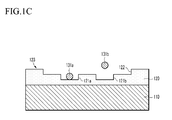
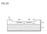
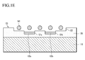
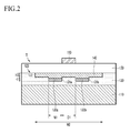
- FIGS. 1A to 1 F and FIG. 2 are cross sectional views to illustrate a method of manufacturing a TFT according to one embodiment of the present invention;
- FIG. 3 is a cross sectional view to illustrate a method of manufacturing a TFT according to another embodiment of the present invention;
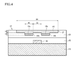
- FIG. 4 is a cross sectional view of a TFT according to still another embodiment of the present invention; and
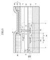
- FIG. 5 is a cross sectional view of a display device employing the TFT according to the one embodiment of the present invention.
- Hereinafter, preferred embodiments of the present invention will be described in detail with reference to the accompanying drawings.
- First, a method of manufacturing a TFT according to the first embodiment of the present invention will be described with reference to FIGS. 1A to 1 F and FIG. 2.
- Referring to FIG. 1A, an organic
insulating film 120 is coated on asubstrate 110. Thesubstrate 110 can be made of insulating material such as glass or plastic or metal material such as stainless steel (SUS). The plastic can be polyethylene terephthalate (PET), polyethylene naphthalate (PEN), polyether sulfone (PES), polyether imide, polyphenylene sulfide (PPS), polyarylate(PAR), polyimide, polycarbonate (PC), polyacrylate, cellulose triacetate and cellulose acetate propionate (CAP), etc. The organicinsulating film 120 can be made of negative type photoresist. - Referring to FIG. 1B, the organic
insulating film 120 is exposed using ahalf tone mask 210 and the exposed organicinsulating film 120 is developed, to form abank 123 having first, second and thirdconcave portions insulating film 120. - The first and second
concave portions drain electrodes - The width W1 of the first and second
concave portions drain electron materials - The height H 1 of the first and second
concave portions drain electron materials drain electron materials concave portions - The distance D1 between the first and second
concave portions - The third
concave portion 122 is a region in which an active layer 140 (refer to FIG. 1 F) will be located and has a rectangular section. - The width W2 of the third
concave portion 122 can be determined according to the width W1 of the first and secondconcave portions - The height H2 of the third
concave portion 122 can be 10 to 1000 nm so that an organic semiconductor material 141 (refer to FIG. 1E) is not overflowed when flowing theorganic semiconductor material 141 and following processes for forming layers can be easily preformed. - The
half tone mask 210 can be composed of light-shield regions transmission regions transmission regions - As in this embodiment, when the organic insulating
film 120 is made of the negative type photoresist, portions not exposed are removed in developing. Accordingly, with thehalf tone mask 210 arranged such that the light-shield regions concave portions transmission regions concave portion 122 except the first and secondconcave portions transmission regions concave portions film 120 can be exposed. - Alternatively, the organic insulating
film 120 can be made of positive type photoresist. In this case, contrary to the above-described embodiment, exposed portions are removed in developing. Accordingly, as shown in FIG. 3, with ahalf tone mask 220 arranged such that light-transmission regions 221 a and 221 b correspond to the first and secondconcave portions transmission regions concave portion 122 except the first and secondconcave portions shield regions concave portions film 120 may be exposed. - Referring to FIG. 1C, source and
drain electrode materials concave portions bank 123, respectively, using an ink-jet method. - Here, the drop quantity of the source and
drain electrode materials concave portions - The source and
drain electrode materials - Alternatively, the source and
drain electrode materials active layer 140 to be formed later. For example, the metal nano particles can be Ag nano particles, Cu nano particles, Au nano particles, Pt nano particles, etc. - Next, a curing process such as ultraviolet curing and thermal curing is performed to evaporate solvent contained in the source and
drain electrode materials drain electrode materials - At this time, since the source and
drain electrode materials bank 123, there does not occur a so-called coffee stain effect that an edge of a pattern becomes thicker than other portions. - As a result, as shown in FIG. 1D, source and
drain electrodes concave portions bank 123 in the organic insulatingfilm 120. - Referring to FIG. 1 E, an
organic semiconductor material 141 is dropped on the thirdconcave portion 122 using an ink-jet method. - Here, the drop quantity of the
organic semiconductor material 141 can be approximately 1 × 10-12 ℓ. However, this quantity for application is not limitative and may be appropriately adjusted depending the width and height of the thirdconcave portion 122. - The
organic semiconductor material 141 can be pentacene, tetracene, anthracene, naphthalene, α-6-thiopene, α-4-thiopene, perylene and derivatives thereof, rubrene and derivatives thereof, coronene and derivatives thereof, perylene tetracarboxylic diimide and derivatives thereof, perylene tetracarboxylic dianhydride and derivatives thereof, polyparaperylenevinylene and derivatives thereof, polyfluorene and derivatives thereof, polyparapheylene and derivatives thereof, olygoacene of naphthalene and derivatives thereof, olygoacene of α-5-thiopene and derivatives thereof, pyromellitic dianhydride and derivatives thereof, pyromellitic diimide and derivatives thereof, perylene tetracarboxylic acid dianhydride and derivatives thereof, phthalocyanine and derivatives thereof, naphthalene tetracarboxylic diimide and derivatives thereof, naphthalene tetracarboxylic dianhydride and derivatives thereof, conjugated polymer derivatives containing substituted or non-substituted thiophene, conjugated polymer derivatives containing substituted fluorine, etc. - Next, a curing process such as ultraviolet curing and thermal curing is performed to evaporate solvent contained in the
organic semiconductor material 141 while flowing theorganic semiconductor material 141. Thus, as shown in FIG. 1F, theactive layer 140 is formed in such a manner that it fills the thirdconcave portion 122 of thebank 123 while contacting the source anddrain electrodes film 120. - Next, a
gate insulating film 150 is formed over the entire surface of thesubstrate 110, a gate electrode material is deposited on thegate insulating film 150 and is patterned to form agate electrode 160, thereby forming a TFT "T" having a structure shown in FIG. 2. - The
gate insulating film 150 can be made of an organic insulating material such as benzocyclobutene (BCB), polyimide, polyvinyphenol or parylene. The gate electrode material can be Ag, Cu, Au, Pt, Mo, MoW, Al, AlNdCr, Al/Cr, etc. - Thus, in the method of manufacturing the TFT according to this embodiment, the
bank 123 is formed in the organic insulatingfilm 120 using thehalf tone mask 210, the source anddrain electrodes active layer 140 are positioned in thebank 123 and are formed in such a manner that they fill in the organic insulatingfilm 120 using the ink-jet method. - Accordingly, a additional patterning process for forming the source and
drain electrodes active layer 140 may be excluded to simplify a process of manufacturing the TFT, and moreover, the coffee stain effect may be prevented to attain good pattern precision, thus avoiding cross-talk between TFTs. - While it has been illustrated in this embodiment that the
gate electrode 160 is formed over theactive layer 140, with thegate insulating film 150 disposed between thegate electrode 160 and theactive layer 140, and the source anddrain electrodes active layer 140, the formation position of thegate electrode 160 is not limited to this embodiment. - For example, as shown in FIG. 4, even a case where a
gate electrode 165 is formed below anactive layer 145, with agate insulating film 155 disposed between thegate electrode 165 and theactive layer 145, and source anddrain electrodes active layer 145, the source anddrain electrodes active layer 145 may be formed in such a manner that they fill in an organicinsulating film 125. - Hereinafter, a display device employing the TFT according to the above embodiment of the present invention will be described with reference to FIG. 5. In this embodiment, an organic light emitting display is exemplified as the display device, and the same components as FIG. 2 are denoted by the same reference numerals in FIG. 5, and therefore, detailed explanation thereof will be omitted.
- Referring to FIG. 5, the TFT "T" shown in FIG. 2 is formed as a driving device on the
substrate 110, a light emitting element "L" to be connected to a portion of the TFT "T" is formed on the TFT "T", with aplanarizing film 170 disposed therebetween, thereby completing pixels. - The
substrate 110 can be made of insulating material such as glass or plastic, or metal material such as stainless steel (SUS). The plastic can be polyethylene terephthalate (PET), polyethylene naphthalate (PEN), polyether sulfone (PES), polyether imide, polyphenylene sulfide (PPS), polyarylate, polyimide, polycarbonate (PC), polyacrylate (PAR), cellulose triacetate and cellulose acetate propionate (CAP), etc. - The light emitting element "L" has a structure where a
first electrode 310, an organiclight emitting layer 330 and asecond electrode 340 are stacked in order, and can be connected to a portion of the TFT "T", for example, thedrain electrode 130b, viaholes gate insulating film 150 and theplanarizing film 170, respectively. Thefirst electrode 310 is isolated from first electrodes (not shown) of adjacent pixels by apixel definition layer 320, and contacts the organiclight emitting layer 330 via anopening 321 provided in thepixel definition film 320. - The
first electrode 310 and thesecond electrode 340 can be made of one or more of ITO (Indium Tin Oxide), IZO (Indium Zinc Oxide), Al, Mg-Ag, Ca, Ca/Ag and Ba. - The organic
light emitting layer 330 can be a low molecule organic material such as copper phthalocyanine (CuPc), N,N'-Di(naphthalene-1-yl)-N,N'-diphenylbenzidine (NPB), tris-8-hydroxyquinoline aluminum (Alq3), etc., or alternatively, a high molecule organic material. - For example, if the organic
light emitting layer 330 is made of the low molecule organic material, it has a multi-layered structure including a hole injection layer (HIL), a hole transport layer (HTL), an emitting layer (EML) and an electron transport layer (ETL). - Alternatively, if the organic
light emitting layer 330 is made of the high molecule organic material, it has the hole transport layer (HTL) and the emitting layer (EML). In this case, the HTL is made of PEDOT material and the EML is made of poly-phenylenevinylene (PPV) type or polyfluorene type material. - Although not shown, the pixels are arranged on the
substrate 110 in the form of a matrix, composing a display unit, sealed and protected by a seal substrate, on which light emission and display are actually conducted. - While it has been illustrated in this embodiment that the TFT "T" shown in FIG. 2 applied as the driving device of the organic light emitting display, it may be applied as driving devices of other display devices such as a liquid crystal display device and so on.
Claims (16)
- A thin film transistor comprising:a gate insulating film;a gate electrode formed on one side of said gate insulating film;an organic insulating film formed on the other side of said gate insulating film; anda source electrode, a drain electrode, and an active layer which are formed to fill in said organic insulating film,the organic insulating film including a bank in which the source electrode, the drain electrode and the active layer are positioned.
- The thin film transistor of claim 1, wherein the bank includes first and second concave portions in which said source electrode and said drain electrode are positioned respectively, and a third concave portion in which said active layer is positioned, said third concave portion being formed on said first and second concave portions.
- The thin film transistor of claim 1, wherein said organic insulating film is made of a negative type photoresist or a positive type photoresist.
- The thin film transistor of claim 1, wherein said active layer is made of an organic semiconductor material.
- The thin film transistor of claim 2, wherein said first and second concave portions include the width of 1 to 50 µm and the height of 50 to 500 nm,
a distance between said first and second concave portions is 1 to 100 µm, and
said third concave portion has the width of 3 to 400 µm and the height of 10 to 1000 nm. - A method of manufacturing a thin film transistor, comprising:forming an organic insulating film on a substrate;forming a bank including first, second and third concave portions in said organic insulating film, the third concave portion being formed on said first and second concave portions;forming a source electrode and a drain electrode in said first and second concave portions; andforming an active layer in said third concave portion, said active layer contacting said source electrode and said drain electrode.
- The method of claim 6, wherein the bank is formed by exposing said organic insulating film using a half tone mask and developing the exposed organic insulating film.
- The method of claim 7, wherein the organic insulating film is made of a negative type photoresist or a positive type photoresist.
- The method of claim 7, wherein said source electrode and said drain electrode are formed by dropping source and drain electrode material in said first and second concave portions using an ink-jet method and curing the substrate on which said source and drain electrode material is dropped.
- The method of claim 9, wherein said source and drain electrode material includes at least one selected from the group consisting of polyethylene dioxythiophene (PEDOT), polyaniline (PANI), conductive high molecules, Ag nano composite, Cu nano composite, Au nano composite, and Pt nano composite, or
includes material formed by pattern-coating and firing material containing metal nano particles or carbon nano particles and organic binders, the metal nano particles or the carbon nano particles having a work function value larger than a value resulting from a subtraction of 0.5 eV from a highest occupied molecular orbital value of material composing the active layer, and
wherein the metal nano particles includes at least one of Ag nano particles, Cu nano particles, Au nano particles and Pt nano particles. - The method of claim 7, wherein the active layer is formed by dropping organic semiconductor material in said third concave portion using an ink-jet method and curing the substrate on which the organic semiconductor material is applied.
- The method of claim 11, wherein said organic semiconductor material include at least one selected from the group consisting of pentacene, tetracene, anthracene, naphthalene, α-6-thiopene, α-4-thiopene, perylene and derivatives thereof, rubrene and derivatives thereof, coronene and derivatives thereof, perylene tetracarboxylic diimide and derivatives thereof, perylene tetracarboxylic dianhydride and derivatives thereof, polyparaperylenevinylene and derivatives thereof, polyfluorene and derivatives thereof, polyparapheylene and derivatives thereof, olygoacene of naphthalene and derivatives thereof, olygoacene of α-5-thiopene and derivatives thereof, pyromellitic dianhydride and derivatives thereof, pyromellitic diimide and derivatives thereof, perylene tetracarboxylic acid dianhydride and derivatives thereof, phthalocyanine and derivatives thereof, naphthalene tetracarboxylic diimide and derivatives thereof, naphthalene tetracarboxylic dianhydride and derivatives thereof, conjugated polymer derivatives containing substituted or non-substituted thiophene, and conjugated polymer derivatives containing substituted fluorine.
- The method of claim 7, wherein said first and second concave portions of the bank have the width of 1 to 50 µm and the height of 50 to 500 nm,
a distance between said first and second concave portions is 1 to 100 µm, and
said third concave portion has the width of 3 to 400 µm and the height of 10 to 1000 nm. - A display device comprising:a substrate;a thin film transistor as claimed in one of the claims 1-5 formed on said substrate; anda light emitting device connected to said thin film transistor.
- The display device of claim 14, wherein said light emitting device has a structure where a first electrode, an organic light emitting layer and a second electrode are stacked in order.
- The display device of claim 14, wherein said substrate comprises insulating material of any one of glass, plastic, and metal material including stainless steel.
Applications Claiming Priority (2)
| Application Number | Priority Date | Filing Date | Title |
|---|---|---|---|
| KR1020050018164A KR100649189B1 (en) | 2005-03-04 | 2005-03-04 | Method for manufacturing organic thin film transistor, organic thin film transistor manufactured by this method, and flat panel display device comprising the organic thin film transistor |
| KR1020060012088A KR100749502B1 (en) | 2006-02-08 | 2006-02-08 | Method for manufacturing thin film transistor, thin film transistor manufactured by this method and display device comprising the thin film transistor |
Publications (2)
| Publication Number | Publication Date |
|---|---|
| EP1701393A1 true EP1701393A1 (en) | 2006-09-13 |
| EP1701393B1 EP1701393B1 (en) | 2014-05-21 |
Family
ID=36571938
Family Applications (1)
| Application Number | Title | Priority Date | Filing Date |
|---|---|---|---|
| EP06110603.5A Ceased EP1701393B1 (en) | 2005-03-04 | 2006-03-02 | Organic thin film transistor and method of manufacturing thereof |
Country Status (3)
| Country | Link |
|---|---|
| US (1) | US7595502B2 (en) |
| EP (1) | EP1701393B1 (en) |
| JP (1) | JP4455517B2 (en) |
Families Citing this family (13)
| Publication number | Priority date | Publication date | Assignee | Title |
|---|---|---|---|---|
| US20060139342A1 (en) * | 2004-12-29 | 2006-06-29 | Gang Yu | Electronic devices and processes for forming electronic devices |
| KR100647695B1 (en) * | 2005-05-27 | 2006-11-23 | 삼성에스디아이 주식회사 | Organic thin film transistor, manufacturing method thereof and flat panel display device having same |
| US8138075B1 (en) | 2006-02-06 | 2012-03-20 | Eberlein Dietmar C | Systems and methods for the manufacture of flat panel devices |
| CN101361192B (en) | 2006-12-18 | 2010-06-02 | 松下电器产业株式会社 | Semiconductor device with a plurality of semiconductor chips |
| KR100927296B1 (en) | 2007-05-28 | 2009-11-18 | 파나소닉 주식회사 | Organic EL Devices and Displays |
| JP5256831B2 (en) * | 2008-04-14 | 2013-08-07 | ソニー株式会社 | Display element, display device, and method of manufacturing display element |
| CN101993032B (en) * | 2009-08-14 | 2013-03-27 | 京东方科技集团股份有限公司 | Method for manufacturing microstructural film pattern and TFT-LCD array substrate |
| JP5493881B2 (en) * | 2010-01-07 | 2014-05-14 | セイコーエプソン株式会社 | Electro-optical device substrate and manufacturing method thereof, electro-optical device, and electronic apparatus |
| US20120280368A1 (en) * | 2011-05-06 | 2012-11-08 | Sean Matthew Garner | Laminated structure for semiconductor devices |
| KR101381353B1 (en) * | 2012-07-06 | 2014-04-04 | 삼성디스플레이 주식회사 | Organic light emitting display device and method of manufacturing the same |
| US9502435B2 (en) * | 2015-04-27 | 2016-11-22 | International Business Machines Corporation | Hybrid high electron mobility transistor and active matrix structure |
| JP6902403B2 (en) * | 2017-06-07 | 2021-07-14 | 矢崎総業株式会社 | Terminal |
| KR20200006647A (en) * | 2018-07-10 | 2020-01-21 | 삼성디스플레이 주식회사 | Display apparatus |
Citations (2)
| Publication number | Priority date | Publication date | Assignee | Title |
|---|---|---|---|---|
| WO2004030072A1 (en) * | 2002-09-25 | 2004-04-08 | Konica Minolta Holdings, Inc. | Electric circuit, thin film transistor, method for manufacturing electric circuit and method for manufacturing thin film transistor |
| US20050026317A1 (en) * | 1999-12-21 | 2005-02-03 | Plastic Logic Limited | Inkjet-fabricated integrated circuits |
Family Cites Families (6)
| Publication number | Priority date | Publication date | Assignee | Title |
|---|---|---|---|---|
| DE10061297C2 (en) | 2000-12-08 | 2003-05-28 | Siemens Ag | Procedure for structuring an OFET |
| JP4841751B2 (en) | 2001-06-01 | 2011-12-21 | 株式会社半導体エネルギー研究所 | Organic semiconductor device and manufacturing method thereof |
| JP4356309B2 (en) | 2002-12-03 | 2009-11-04 | セイコーエプソン株式会社 | Transistors, integrated circuits, electro-optical devices, electronic equipment |
| EP1670079B1 (en) * | 2004-12-08 | 2010-12-01 | Samsung Mobile Display Co., Ltd. | Method of forming a conductive pattern of a thin film transistor |
| KR100649189B1 (en) | 2005-03-04 | 2006-11-24 | 삼성에스디아이 주식회사 | Method for manufacturing organic thin film transistor, organic thin film transistor manufactured by this method, and flat panel display device comprising the organic thin film transistor |
| KR100659125B1 (en) | 2005-12-12 | 2006-12-19 | 삼성에스디아이 주식회사 | Thin film transistor and flat panel display device having same |
-
2006
- 2006-02-28 US US11/363,198 patent/US7595502B2/en active Active
- 2006-02-28 JP JP2006053545A patent/JP4455517B2/en not_active Expired - Fee Related
- 2006-03-02 EP EP06110603.5A patent/EP1701393B1/en not_active Ceased
Patent Citations (2)
| Publication number | Priority date | Publication date | Assignee | Title |
|---|---|---|---|---|
| US20050026317A1 (en) * | 1999-12-21 | 2005-02-03 | Plastic Logic Limited | Inkjet-fabricated integrated circuits |
| WO2004030072A1 (en) * | 2002-09-25 | 2004-04-08 | Konica Minolta Holdings, Inc. | Electric circuit, thin film transistor, method for manufacturing electric circuit and method for manufacturing thin film transistor |
Non-Patent Citations (1)
| Title |
|---|
| DE LEEUW D M ET AL: "Polymeric integrated circuits and light-emitting diodes", ELECTRON DEVICES MEETING, 1997. TECHNICAL DIGEST., INTERNATIONAL WASHINGTON, DC, USA 7-10 DEC. 1997, NEW YORK, NY, USA,IEEE, US, 7 December 1997 (1997-12-07), pages 331 - 336, XP010265518, ISBN: 0-7803-4100-7 * |
Also Published As
| Publication number | Publication date |
|---|---|
| US7595502B2 (en) | 2009-09-29 |
| JP2006245582A (en) | 2006-09-14 |
| US20060197079A1 (en) | 2006-09-07 |
| JP4455517B2 (en) | 2010-04-21 |
| EP1701393B1 (en) | 2014-05-21 |
Similar Documents
| Publication | Publication Date | Title |
|---|---|---|
| US8030642B2 (en) | Organic thin film transistor, method of manufacturing the same, and flat panel display having the same | |
| US8318533B2 (en) | Method of manufacturing an organic thin film transistor | |
| US8222631B2 (en) | Organic thin film transistor and flat display device having the same | |
| KR100659061B1 (en) | Organic thin film transistor and flat panel display device having same | |
| US7667385B2 (en) | Organic thin film transistor and organic electroluminescent device using the same | |
| US7910401B2 (en) | Organic thin film transistor, flat panel display apparatus comprising the same, and method of manufacturing the organic thin film transistor | |
| CN1819299B (en) | Thin film transistors, flat panel display including the thin film transistor and method for manufacturing the thin film transistor and the flat panel display | |
| EP1701393B1 (en) | Organic thin film transistor and method of manufacturing thereof | |
| CN1832220B (en) | Method for manufacturing thin film transistor, thin film transistor and display device | |
| KR100730159B1 (en) | Organic thin film transistor, flat panel display having same, manufacturing method of organic thin film transistor | |
| US7601567B2 (en) | Method of preparing organic thin film transistor, organic thin film transistor, and organic light-emitting display device including the organic thin film transistor | |
| US8076733B2 (en) | Flat panel display device having an organic thin film transistor and method of manufacturing the same | |
| US7714324B2 (en) | Organic thin film transistor and method of manufacturing the same | |
| US20070290196A1 (en) | Organic light emitting display device and method for manufacturing the organic light emitting display device | |
| KR100749502B1 (en) | Method for manufacturing thin film transistor, thin film transistor manufactured by this method and display device comprising the thin film transistor | |
| US20070114920A1 (en) | Organic thin film transistor, method of manufacturing the same, and flat display apparatus comprising the same | |
| KR100822209B1 (en) | Manufacturing Method of Organic Light Emitting Display | |
| KR100719569B1 (en) | Flat panel display device | |
| KR100807558B1 (en) | Organic thin film transistor, manufacturing method thereof and organic light emitting device comprising the same |
Legal Events
| Date | Code | Title | Description |
|---|---|---|---|
| PUAI | Public reference made under article 153(3) epc to a published international application that has entered the european phase |
Free format text: ORIGINAL CODE: 0009012 |
|
| 17P | Request for examination filed |
Effective date: 20060302 |
|
| AK | Designated contracting states |
Kind code of ref document: A1 Designated state(s): AT BE BG CH CY CZ DE DK EE ES FI FR GB GR HU IE IS IT LI LT LU LV MC NL PL PT RO SE SI SK TR |
|
| AX | Request for extension of the european patent |
Extension state: AL BA HR MK YU |
|
| 17Q | First examination report despatched |
Effective date: 20060929 |
|
| AKX | Designation fees paid |
Designated state(s): DE FR GB |
|
| RAP1 | Party data changed (applicant data changed or rights of an application transferred) |
Owner name: SAMSUNG MOBILE DISPLAY CO., LTD. |
|
| RAP1 | Party data changed (applicant data changed or rights of an application transferred) |
Owner name: SAMSUNG DISPLAY CO., LTD. |
|
| REG | Reference to a national code |
Ref country code: DE Ref legal event code: R079 Ref document number: 602006041650 Country of ref document: DE Free format text: PREVIOUS MAIN CLASS: H01L0051400000 Ipc: H01L0051050000 |
|
| GRAP | Despatch of communication of intention to grant a patent |
Free format text: ORIGINAL CODE: EPIDOSNIGR1 |
|
| INTG | Intention to grant announced |
Effective date: 20140106 |
|
| RIC1 | Information provided on ipc code assigned before grant |
Ipc: H01L 51/40 20060101ALI20131216BHEP Ipc: H01L 51/05 20060101AFI20131216BHEP |
|
| GRAS | Grant fee paid |
Free format text: ORIGINAL CODE: EPIDOSNIGR3 |
|
| GRAA | (expected) grant |
Free format text: ORIGINAL CODE: 0009210 |
|
| AK | Designated contracting states |
Kind code of ref document: B1 Designated state(s): DE FR GB |
|
| REG | Reference to a national code |
Ref country code: GB Ref legal event code: FG4D |
|
| REG | Reference to a national code |
Ref country code: DE Ref legal event code: R096 Ref document number: 602006041650 Country of ref document: DE Effective date: 20140626 |
|
| REG | Reference to a national code |
Ref country code: DE Ref legal event code: R097 Ref document number: 602006041650 Country of ref document: DE |
|
| PLBE | No opposition filed within time limit |
Free format text: ORIGINAL CODE: 0009261 |
|
| STAA | Information on the status of an ep patent application or granted ep patent |
Free format text: STATUS: NO OPPOSITION FILED WITHIN TIME LIMIT |
|
| 26N | No opposition filed |
Effective date: 20150224 |
|
| REG | Reference to a national code |
Ref country code: DE Ref legal event code: R097 Ref document number: 602006041650 Country of ref document: DE Effective date: 20150224 |
|
| REG | Reference to a national code |
Ref country code: FR Ref legal event code: PLFP Year of fee payment: 11 |
|
| REG | Reference to a national code |
Ref country code: FR Ref legal event code: PLFP Year of fee payment: 12 |
|
| REG | Reference to a national code |
Ref country code: FR Ref legal event code: PLFP Year of fee payment: 13 |
|
| REG | Reference to a national code |
Ref country code: DE Ref legal event code: R079 Ref document number: 602006041650 Country of ref document: DE Free format text: PREVIOUS MAIN CLASS: H01L0051050000 Ipc: H10K0010000000 |
|
| P01 | Opt-out of the competence of the unified patent court (upc) registered |
Effective date: 20230515 |
|
| PGFP | Annual fee paid to national office [announced via postgrant information from national office to epo] |
Ref country code: DE Payment date: 20240220 Year of fee payment: 19 Ref country code: GB Payment date: 20240220 Year of fee payment: 19 |
|
| PGFP | Annual fee paid to national office [announced via postgrant information from national office to epo] |
Ref country code: FR Payment date: 20240226 Year of fee payment: 19 |
|
| REG | Reference to a national code |
Ref country code: DE Ref legal event code: R119 Ref document number: 602006041650 Country of ref document: DE |
|
| GBPC | Gb: european patent ceased through non-payment of renewal fee |
Effective date: 20250302 |
|
| PG25 | Lapsed in a contracting state [announced via postgrant information from national office to epo] |
Ref country code: DE Free format text: LAPSE BECAUSE OF NON-PAYMENT OF DUE FEES Effective date: 20251001 |
|
| PG25 | Lapsed in a contracting state [announced via postgrant information from national office to epo] |
Ref country code: GB Free format text: LAPSE BECAUSE OF NON-PAYMENT OF DUE FEES Effective date: 20250302 |
|
| PG25 | Lapsed in a contracting state [announced via postgrant information from national office to epo] |
Ref country code: FR Free format text: LAPSE BECAUSE OF NON-PAYMENT OF DUE FEES Effective date: 20250331 |