EP1688975A1 - Capacitor - Google Patents
Capacitor Download PDFInfo
- Publication number
- EP1688975A1 EP1688975A1 EP04819404A EP04819404A EP1688975A1 EP 1688975 A1 EP1688975 A1 EP 1688975A1 EP 04819404 A EP04819404 A EP 04819404A EP 04819404 A EP04819404 A EP 04819404A EP 1688975 A1 EP1688975 A1 EP 1688975A1
- Authority
- EP
- European Patent Office
- Prior art keywords
- current collector
- positive electrode
- negative electrode
- element assembly
- tab portion
- Prior art date
- Legal status (The legal status is an assumption and is not a legal conclusion. Google has not performed a legal analysis and makes no representation as to the accuracy of the status listed.)
- Withdrawn
Links
Images




Classifications
-
- H—ELECTRICITY
- H01—ELECTRIC ELEMENTS
- H01G—CAPACITORS; CAPACITORS, RECTIFIERS, DETECTORS, SWITCHING DEVICES, LIGHT-SENSITIVE OR TEMPERATURE-SENSITIVE DEVICES OF THE ELECTROLYTIC TYPE
- H01G9/00—Electrolytic capacitors, rectifiers, detectors, switching devices, light-sensitive or temperature-sensitive devices; Processes of their manufacture
- H01G9/004—Details
- H01G9/08—Housing; Encapsulation
- H01G9/10—Sealing, e.g. of lead-in wires
-
- H—ELECTRICITY
- H01—ELECTRIC ELEMENTS
- H01G—CAPACITORS; CAPACITORS, RECTIFIERS, DETECTORS, SWITCHING DEVICES, LIGHT-SENSITIVE OR TEMPERATURE-SENSITIVE DEVICES OF THE ELECTROLYTIC TYPE
- H01G11/00—Hybrid capacitors, i.e. capacitors having different positive and negative electrodes; Electric double-layer [EDL] capacitors; Processes for the manufacture thereof or of parts thereof
- H01G11/66—Current collectors
- H01G11/70—Current collectors characterised by their structure
-
- H—ELECTRICITY
- H01—ELECTRIC ELEMENTS
- H01G—CAPACITORS; CAPACITORS, RECTIFIERS, DETECTORS, SWITCHING DEVICES, LIGHT-SENSITIVE OR TEMPERATURE-SENSITIVE DEVICES OF THE ELECTROLYTIC TYPE
- H01G11/00—Hybrid capacitors, i.e. capacitors having different positive and negative electrodes; Electric double-layer [EDL] capacitors; Processes for the manufacture thereof or of parts thereof
- H01G11/74—Terminals, e.g. extensions of current collectors
-
- H—ELECTRICITY
- H01—ELECTRIC ELEMENTS
- H01G—CAPACITORS; CAPACITORS, RECTIFIERS, DETECTORS, SWITCHING DEVICES, LIGHT-SENSITIVE OR TEMPERATURE-SENSITIVE DEVICES OF THE ELECTROLYTIC TYPE
- H01G11/00—Hybrid capacitors, i.e. capacitors having different positive and negative electrodes; Electric double-layer [EDL] capacitors; Processes for the manufacture thereof or of parts thereof
- H01G11/78—Cases; Housings; Encapsulations; Mountings
- H01G11/82—Fixing or assembling a capacitive element in a housing, e.g. mounting electrodes, current collectors or terminals in containers or encapsulations
-
- H—ELECTRICITY
- H01—ELECTRIC ELEMENTS
- H01G—CAPACITORS; CAPACITORS, RECTIFIERS, DETECTORS, SWITCHING DEVICES, LIGHT-SENSITIVE OR TEMPERATURE-SENSITIVE DEVICES OF THE ELECTROLYTIC TYPE
- H01G9/00—Electrolytic capacitors, rectifiers, detectors, switching devices, light-sensitive or temperature-sensitive devices; Processes of their manufacture
- H01G9/15—Solid electrolytic capacitors
- H01G9/151—Solid electrolytic capacitors with wound foil electrodes
-
- Y—GENERAL TAGGING OF NEW TECHNOLOGICAL DEVELOPMENTS; GENERAL TAGGING OF CROSS-SECTIONAL TECHNOLOGIES SPANNING OVER SEVERAL SECTIONS OF THE IPC; TECHNICAL SUBJECTS COVERED BY FORMER USPC CROSS-REFERENCE ART COLLECTIONS [XRACs] AND DIGESTS
- Y02—TECHNOLOGIES OR APPLICATIONS FOR MITIGATION OR ADAPTATION AGAINST CLIMATE CHANGE
- Y02E—REDUCTION OF GREENHOUSE GAS [GHG] EMISSIONS, RELATED TO ENERGY GENERATION, TRANSMISSION OR DISTRIBUTION
- Y02E60/00—Enabling technologies; Technologies with a potential or indirect contribution to GHG emissions mitigation
- Y02E60/13—Energy storage using capacitors
Definitions
- the present invention relates to a capacitor, in particular, to a capacitor which can reduce a resistance between an element assembly and terminals even when terminals are provided only on one side of an outer casing, which can reduce inductance, and which can reduce time for producing the element assembly.
- Electric double layer capacitors and electrolytic capacitors have each a current collection structure for collecting current from an element assembly in the inside and for electrically connecting the element assembly with terminals for external connection.
- Fig. 7 shows a vertically cross-sectional view of an electric double layer capacitor having a conventional current collection structure.
- Fig. 8 shows a constructional view of a conventional element assembly
- Fig. 9 shows a view observed from an allow A of Fig. 8 (a separator is omitted).
- Patent document 1 is known, which describes a capacitor having such a current collection structure.
- a column-shaped element assembly 1 impregnated with an electrolytic solution is accommodated in a cylindrical outer casing 21 having a bottom portion 21a, and an opening 21b of the outer casing 21 is sealed with a sealing plate 31.
- the element assembly 1 is constituted by a pair of long band-shaped electrode bodies 3A and 3B, and separators 5A and 5B disposed between the electrode bodies 3A and 3B so as to be laminated together, and the element assembly 1 is formed by winding these electrode bodies 3A and 3B and separators 5A and 5B.
- one of the electrode bodies 3A and 3B constitute a positive electrode and the other constitutes a negative electrode.
- the electrode bodies 3A and 3B have current collector foils 7A and 7B respectively that are made of a metal and having a large length, and electrode layers 9A and 9B formed on the surfaces of the electric collector foils 7A and 7B respectively.
- electrode layers 9A and 9B for example, a material having a large specific surface area such as an activated carbon to form electric double layer in the electric collector foils 7A and 7B to develop current storage function.
- electrode layers 9A and 9B are formed only on one side of the electric collector foils 7A and 7B respectively in Fig. 9, however, they may be formed on both sides.
- tab-bonding portions 11A and 11B are formed respectively so as to each extend along the full length of the axial direction of the roll of the element assembly 1, in which no electrode layer 9A or 9B is formed.
- band-shaped tabs 13A and 13B and current collector foils 7A and 7B are bonded respectively by press-bonding or vibration bonding in a state that protrusions 15A and 15B that are ends of the tabs 13A and 13B respectively are protruded outwardly from the electrode bodies 3A and 3B respectively.
- the positions of the current collector foils 7A and 7B to bond the tabs 13A and 13B respectively are determined so as to sufficiently isolate each other the protrusions 15A and 15B connected to the electrode bodies 3A and 3B respectively having opposite polarities to each other, in a state that a cylindrical element assembly 1 is formed.
- the protrusions 15A and 15B of the tabs 13A and 13B protrude in a state that they are isolated from each other, so that they are connected with terminals 33A and 33B respectively attached to through holes 31a and 31a perforating through the sealing plate 31.
- the single cell 50 is used for an electric double layer capacitor or a large-sized electrolytic capacitor, it is necessary to reduce the resistance of the single cell 50 to suppress heat generation of the single cell 50 itself.
- Patent Document 2 requires a precondition that bus bars corresponding to the terminals 33A and 33B are disposed on the respective end faces of a module casing.
- a single cell having the electric collection structure of Patent Document 2 does not have a construction that terminals 33A and 33B are disposed only on one side that is the side of the opening 21b of the outer casing 21, and there has been a possibility that wiring becomes complicated in a case of wiring single cells together or wiring a single cell with an external circuit, and thus, there has been a possibility that space saving is difficult.
- the present invention has been made considering the above conventional problems, and it is an object of the present invention to provide a capacitor which can reduce the resistance from an element assembly to terminals even when the terminals are provided only on one side of the outer casing, which can reduce inductance, and which can reduce time for producing the element assembly.
- the present invention provides a capacitor comprising an electrolytic solution; a column-shaped element assembly including a positive electrode, a negative electrode and a separator, each of the positive electrode and the negative electrode having a long current collector foil and having an end strip portion extending along an entire length of one side of the current collector foil in a longitudinal direction, the positive electrode and the negative electrode being electrode bodies disposed so as to be opposed to each other, the separator separating the positive electrode and the negative electrode and having ion permeability, wherein the positive electrode, the negative electrode and the separator are wound such that the positive electrode and the negative electrode have at least one portion of the end strip portions projecting from the separator in opposite directions; an outer casing for accommodating the element assembly and the electrolytic solution and having an opening formed at one end; a positive electrode current collector and a negative electrode current collector respectively disposed at both ends of the element assembly, the positive electrode current collector being electrically connected to the end strip portion of the positive electrode, the negative electrode collector being electrically connected to the end strip portion of the negative electrode; a
- the positive and negative electrodes are configured so that the end strip portions of the respective current collector foils are positioned at opposite ends of the element assembly to each other. Further, between the positive electrode current collector plate and the positive terminal, and between the negative electrode current collector plate and the negative terminal, the positive tab portion and the negative tab portion are provided respectively, and the positive electrode terminal and the negative electrode terminal are attached to the respective through holes perforating through the sealing plate sealing the outer casing, and thus, it is possible to input and output electric energy from the element assembly to the outside at one side of the outer casing. Accordingly, in a case of connecting outer casings (single cells) each accommodating an element assembly, to each other or in a case of wiring between a single cell and an external circuit, it is possible to make such wirings simple and to facilitate space saving.
- the element assembly of the present invention there is no need of considering bonding positions of tabs, that have been required in conventional element assemblies. Accordingly, there is no need of momentary stopping winding of the element assembly, and thus it is possible to reduce time for producing the element assembly. Further, in the element assembly of the present invention, instead of conventional bonding of tabs, only connections of a positive electrode current collector plate and a negative electrode current collector plate are required after the winding step of the element assembly, the manufacturing becomes simple, and accordingly, production cost of capacitors can be reduced.
- the positive electrode current collector and the negative electrode current collector are disposed in a direction in parallel with a winding cross-section of the element assembly.
- each current collector plate is in contact with the end strip portion of the electrode assembly in full length of the end strip portion, it is possible to reduce the resistance between the electrode body and the current collector plate, it is possible to reduce inductance and it is possible to reduce the resistance of entire capacitor.
- influence of inductance increases as a resistance factor, and thus, application of the structure of the present invention remarkably contribute to reduce the resistance of entire capacitor at a time of charging or discharging a large current in a short time of at most 1 second.
- the positive electrode tab portion or the negative electrode tab portion that is connected to the current collector disposed on the side opposite from the sealing plate is disposed so as to pass through a gap between the outermost peripheral portion of the element assembly and the outer casing.
- a current collector plate which is not in proximity with the positive electrode terminal and the negative electrode terminal attached to the through holes namely, a current collector plate disposed on the opposite side from the sealing plate, is connected with a tab portion connected with the positive electrode terminal or the negative electrode terminal through a gap between the outermost periphery of the element assembly and the outer casing.
- the length of the positive tab portion or the negative tab portion becomes relatively long.
- the positive electrode tab portion or the negative electrode tab portion is disposed between the outermost periphery of the element assembly and the outer casing, its cross-sectional area can be designed without any restriction so long as it can be accommodated in the outer casing. Accordingly, it is possible to design these members so that their resistances are negligible in the resistance of entire unit, and it is possible to reduce the resistance between the current collector plates and the terminals, and thus, it is possible to reduce the resistance of the capacitor as a whole.
- the end strip portions of the positive electrode and the negative electrode are respectively welded to central portions of the positive electrode current collector and the negative electrode current collector in radial directions with respect to the respective central portions, and further, it is preferred that the positive electrode current collector and the negative electrode current collector each has a shape symmetrical about a point, and the end strip portions of the positive electrode and the negative electrode are welded to the positive electrode current collector and the negative electrode current collector respectively so as to be symmetrical about the respective central portions, and further, it is preferred that the respective central portions of the positive electrode current collector and the negative electrode current collector are welded to an end of the positive electrode tab portion and an end of the negative electrode tab portion respectively.
- the present invention may have such a construction that the positive electrode current collector and the positive electrode tab portion are integrally formed, and the negative electrode current collector and the negative electrode tab portion are integrally formed.
- the capacitor of the present invention is preferably an electric double layer capacitor wherein the positive electrode or the negative electrode has an electrode layer formed on at least one side of the current collector foil except for the end strip portion, the electrode layer being made of a material having a high specific surface area.
- an electric double layer capacitor having efficient electric storage function can be formed.
- the current collector foils are made of aluminum or an aluminum alloy, and the positive electrode has a dense oxide film formed on the current collector foil.
- the present invention even when a positive electrode and a negative electrode are provided only on one side of a casing, it is possible to reduce connection resistances from an element assembly to the positive electrode terminal and the negative electrode terminal, it is possible to reduce inductance, and it is possible to reduce time to produce the element assembly.
- Fig. 1 shows a vertically cross-sectional view of an electric double layer capacitor having the current collection structure as an embodiment of the present invention.
- Fig. 2 shows a construction view of an element assembly of the present invention
- Fig. 3 shows a view observed from an arrow B of Fig. 2.
- elements in common with those of Figs. 7 to 9 have the same reference numerals and their descriptions are omitted.
- a single cell 100 of the electric double capacitor of the present invention has, in the same manner as the conventional single cell 50, a construction that a column shaped element assembly 101 impregnated with an electrolytic solution, not shown, is accommodated in an outer casing 21 and sealed by a sealing plate 31.
- electrode bodies 103A and 103b constituting a positive electrode and a negative electrode respectively of the element assembly 101 of the present invention have a long band shaped current collector foils 107A and 107B respectively, and electrode layers 9A and 9B are formed on both surfaces of the current collector foils 107A and 107B respectively so that they occupy entire surfaces except end strip portions 108A and 108B present along in full length of one side in the direction of their lengths.
- the electrode layers 9A and 9B in the same manner as the conventional electrode bodies 3A and 3B, a material having high specific surface area is employed to form an electric double layer on the current collector foils 107A and 107B to develop electric storage function.
- the electrode layers 9A and 9B are formed on both sides of the electric collector foils 107A and 107B respectively.
- the electrode layers 9A and 9B may be formed on one side of the electric collector foils 107A and 107B respectively. Further, in Fig.
- strip portions 108C and 108D are slightly remaining on opposite sides from the end strip portions 108A and 108B respectively, and the strip portions 108C and 108D show only necessary margins between the electric collector foil 107A and 9A and the electrode layers 107B and 9B respectively for producing the electrode bodies 103A and 103B, and the strip portions 108C and 108D are preferably not provided from the viewpoint of energy density of the element assembly 101.
- the element bodies 103A and 103B are wound so that their respective end strip portions 108A and 108B protrude in the opposite side from each other from the separators 5A and 5B and along the separators 5A and 5B, whereby a column shaped element assembly 101 is formed.
- an insulating member not shown is disposed to cover the electrode body 103A or the electrode body 103B.
- the insulating member is preferably a separator 5.
- the end strip portions 108A and 108B of the electrode members 103A and 103B respectively are independently exposed. Further, the end strip portions 108A and 108B are configured to be bonded with current collector plates 141A and 141B.
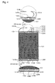
- Fig. 4 includes enlarged views of bonded portions where the element assembly is bonded with the respective current collector plates, and Fig. 5 shows a construction view of the current collector plates.
- the current collector plates 141A and 141B each has a point symmetric shape, and they have disk shaped plates 143A and 143B each having approximately the same area as that of the wound cross section of the element assembly 101, and they are provided in a direction in parallel with the wound cross section. Further, on one surface of each of the plates 143A and 143B, end strip portions 108A and 108B of the electrode bodies 103A and 103B are bonded respectively.
- the bonding of the end strip portions 108A and 108B and the plates 143A and 143B respectively may be carried out by a mechanical pressing or conductive bonding with a conductive adhesive agent, but the bonding is preferably carried out by welding having high mechanical and electrical reliability. Further, as such a welding, an ultrasonic welding, a laser welding by e.g. a YAG laser or an electron beam welding, is preferably employed.
- the welding in order to make the distance from the central portion 145A or 145B of a plate portion 143A or 143B respectively to each welding spots 146A or 146B equal, the welding is preferably carried out in a radial pattern from the central portion towards the outer periphery. For example, as shown in Fig.
- total seven spots are provided in the plate portion 143A or 143B, the seven spots comprises one spot in the central portion (central portion 145A or 145B), and six spots at evenly divided position in the vicinity of the outer periphery of the plate portion 143A or 143B (welding spot 146A or 146B), and line weldings are made from the central portion 145A or 145B to the welding spots 146A or 146B in a radial pattern (the linear welding portions are shown as linear welding portions 148A or 148B in Fig. 5).
- the electrode body 103A or 103B and the electric collector plate 141A or 141B respectively can be entirely in contact, and contact resistance can be reduced, such being preferred.
- the linear welding is made at an angle symmetrical about the symmetric center (central portion 145A or 145B), the contact resistance can be sufficiently reduced, such being preferred.
- a small protrusion 147A or 147B protruding from the central portion of the plate portion 143A or 143B is provided. Further, it is preferred that a punched hole or a notch, not shown, is formed on the plate portion 143A or 143B so as not to prevent the electrolytic solution from impregnating from the end face of the element assembly 101.
- a band shaped short tab portion 151A having one end connected to the electric collector plate 141A is disposed so as to cover the small protrusion 147A.
- the length LA in the longitudinal direction of the short tab portion 151A is made longer than the distance between the small protrusion 147A and the terminal 33A by a predetermined length so as to have a margin for connecting with the terminal 33A when the element assembly 101 is accommodated in the outer casing 21.
- the electric collector plate 141B to be bonded to the end strip portion 108B disposed on the bottom 21a side when the element assembly 101 is accommodated in the outer casing 21, is provided with a band shaped long tab portion 151B having one end connected with the side portion of the small protrusion 147B of the electric collector plate 141B.
- the length LB in the longitudinal direction of the long tab portion 151B is made longer than the length LA of the short tab portion 151A, and longer than the distance to the terminal 33B through the gap between the outer peripheral portion of the element assembly 101 and the outer casing 21 by a predetermined length so as to have a margin for connecting with the terminal 33B when the element assembly 101 is accommodated in the outer casing 21.
- Such a short tab portion 151A and a long tab portion 151B are each designed to have a cross-sectional area so that its resistance becomes sufficiently smaller than the inherent resistance of the element assembly 101 and so as to satisfy the resistance required for the complete single cell 100.
- the element assembly 101 provided with such current collector plates 141A and 141B and a short tab portion 151A and a long tab portion 151B, is accommodated in the outer casing 21 and sealed by the sealing plate 31, the other end of the short tab portion 151A is connected with the terminal 33A attached to a through hole 31a, and the other end of the long tab portion 151B is connected with a terminal 33B attached to a through hole 31b.
- the short tab portion 151A is in a state of arch shape according to the difference between the length of the short tab portion 151A and the distance between the small protrusion 147A and the terminal 33A.
- the long tab portion 151B two bent portions 153 and 154 are formed in this order from the small protrusion 147B so that the long tab portion 151B extends from the small protrusion 147B of the current collector plate 141B through a gap between the outermost periphery of the element assembly 101 and the outer casing 21, to be connected with the terminal 33B.
- the long tab portion 151B is provided so that its longitudinal direction is along a radial direction of the plate portion 143B from the small protrusion 147B to the bent portion 153, and along the axial direction of the roll of the element assembly 101 from the bent portion 153 to the bent portion 154, and further, it is in a state of arch shape from the bent portion 154 to the terminal 33B.
- the long tab portion 151B is disposed between the outermost peripheral portion of the element assembly 101 and the outer casing 21 within the range of from the bent portion 153 to the bent portion 154, and an isolation member, not shown, is provided in the outermost peripheral portion of the element assembly 101 so that no short circuit occurs to e.g. the electrode body 103A or 103B in the element assembly 101. Further, in the vicinity of the bent portion 154 of the long tab portion 151B, the long tab portion 151B is in proximity with the current collector plate 141A connected with the electrode body 103A of the other polarity, and an insulation member, not shown, is interposed in this portion so as to isolate these members from each other.
- the outermost peripheral portion of the element assembly 101 is constituted by a separator 5, it is not necessary to provide an additional isolation member.
- the end strip portions 108A and 108B of the electrode bodies 103A and 103B respectively are exposed from the bottom 21a side and the opening 21b side respectively of the outer casing 21, and the current collector plates 141A and 141B are bonded to the end strip portions 108A and 108B respectively.
- the terminals 33A and 33B are disposed only on the opening 21b side of the outer casing 21, namely, only on the sealing plate 31.
- the long tab portion 151B is relatively long, but its cross-sectional area is designed so that the resistance of the long tab portion 151B becomes sufficiently smaller than the inherent resistance of the element assembly 101 to satisfy the resistance required for a complete single cell 100.
- the cross-sectional area can be designed without any restriction within a range that it can be accommodated in the outer casing 21. Accordingly, the resistance of the long tab portion 151B is negligible to the resistance of entire single cell 100. This feature is also applied to the short tab portion 151A.
- the current collector plates 141A and 141B contact with the terminal strip portions 108A and 108B of the electrode bodies 103A and 103B respectively by the above construction, the resistances between the electrode bodies 103A and 103B and the electric collector plates 141A and 141B respectively, can be reduced. Further, by the above welding, since the welding is formed in a radial pattern from the central portion of each of the plates 143A and 143B towards the outer periphery, inputting and outputting of electric energy can be carried out evenly from the electrode bodies 103A and 103B.
- the long tab portion 151B is provided in the electric collector plate 141B on the bottom 21a side, inputting and outputting of electric energy from the element assembly 101 to the outside can be carried out only on the opening 21b side of the outer casing. Accordingly, in a case of wiring the single cells 100 to each other or in a case of wiring a single cell 100 with outside circuits, wires can be easily connected and space saving can be easily achieved.
- cross-sectional areas of the short tab portion 151A and the long tab portion 151B are designed so that their resistances become negligible to the resistance of entire single cell 100, and thus it is possible to reduce the resistances between the current collector plates 141A and 141B and the terminals 33A and 33B respectively.
- the terminals 33A and 33B can be disposed only on one side of the opening 21b side of the outer casing 21, and the resistances from the element assembly to the terminals 33A and 33B can be reduced.
- the element assembly 101 of the present invention there is no need of considering the boding positions of the tabs 13A and 13B required in the conventional element assembly 1. Therefore, it is not necessary to momentary stop winding of the element assembly 101, and thus, time to produce the element assembly 101 can be reduced.
- the element assembly 101 of the present invention instead of bonding conventional tabs 13A and 13B, only bonding of the current collector plates 141A and 141B have to be carried out separately after the production step of the element assembly 101, and thus, the production step of the element assembly 101 is simple. Accordingly, production cost of the single cell 100 can be reduced.
- the short tab portion 151A and the long tab portion 151B are explained to be connected with small protrusions 147A and 147B of the electric collector plates 141A and 141B respectively.
- the construction is not limited thereto. Namely, so long as the plate portions 143A and 143B of the current collector plates are electrically in contact with the terminals 33A and 33B (refer to Fig. 1) respectively, the short tab portion 151A and the long tab portion 151B may be integrally formed together with the plate portions 143A and 143B respectively of the current collector plate.
- the material of the current collector foils 107A and 107B to be employed for the electrode bodies 103A and 103B constituting the positive and negative electrodes are not particularly limited so long as it is excellent in electrochemical corrosion resistance. However, from the viewpoint of manufacturability and light weight, foils of aluminum, an aluminum alloy or a stainless steel, is preferred.
- the material having high specific surface area to be employed for the electrode layers 9a and 9B contains as the main component a carbon material having a specific surface area of from 100 to 3,000 m 2 /g, and an activated carbon of resin type such as phenol resin, a coconut shell type, a cokes type or a pitch type, or a carbon nano tube, a carbon aero gel, a polyacene or the like may be suitably employed, and as a conductive auxiliary agent, carbon black, a carbon short fiber or a metallic fiber is preferred.
- the electrode layers 9A and 9B to be employed for positive and negative electrodes may be constituted by the same material, or may be constituted by different materials from each other.
- the material of the separators 5A and 5B may be any material so long as it has ion permeability, and is preferably constituted by a porous material excellent in electrical insulation and chemical stability against electrolytic solution and liquid-retaining property which can absorb a large amount of electrolytic solution.
- an inorganic material such as a glass fiber, a silica fiber, an alumina fiber, an asbesto or e.g. a whisker of these materials, or an organic material such as a paper material such as a Manila hemp paper, a cellulose paper, a craft paper or a mixed paper of rayon fiber and sisal hemp, a synthesized polymer fiber such as polyolefin or polyester, is preferred.
- a sheet formed by weaving these materials, a micro porous film provided with fine holes by drawing, or the like is preferred.
- the material of the current collector plates 141A and 141B is preferably the same material as the current collector foils 107A and 107B, and is most preferably aluminum, an aluminum alloy or a stainless steel.
- the material of the short tab portion 151A and the long tab portion 151B is preferably the same material as the current collector foils 107A and 107B, and is most preferably aluminum, an aluminum alloy or a stainless steel.
- the thicknesses of the current collector plate 141A and 141B, short tab portion 151A and the long tab portion 151B are preferably at most 0.8 mm.
- the lengths of the short tab portion 151A and the long tab portion 151B are preferably as short as possible within the acceptable range from the design point of view.
- the material of the terminals 33A and 33B is preferably the same material as the electrode bodies 103A and 103B to reduce the resistance and for bonding with the short tab portion 151A and the long tab portion 151B, and is the most preferably aluminum, an aluminum alloy or a stainless steel, but copper may also be employed for the material.
- the materials of the current collector foils 107A and 107B are both aluminum or an aluminum alloy, and the current collector foil 107A is an etched foil for negative electrode, and the current collector foil 107B is an etched foil for positive electrode, and there is no need of providing the electrode layers 9A and 9B.
- the positive electrode is one constituted by a current collector foil 107B on which a dense oxide film is formed.
- the negative electrode is preferably constituted by a current collector foil 107A that is subjected to an extension treatment and a stabilization treatment to form a thin film.
- the resistance from the element assembly 101 to the terminals 33A and 33B can be reduced to at most 1/5 of the resistance of the single cell 50.
- connection resistances from an element assembly to the positive electrode terminal and the negative electrode terminal can be reduced, and inductance can be reduced, and further, time to produce the element assembly can be reduced, whereby the present invention can be applied to a capacitor, an electric double layer capacitor or an aluminum electrolytic capacitor.
Landscapes
- Engineering & Computer Science (AREA)
- Power Engineering (AREA)
- Microelectronics & Electronic Packaging (AREA)
- Electric Double-Layer Capacitors Or The Like (AREA)
- Connection Of Batteries Or Terminals (AREA)
Abstract
Description
- The present invention relates to a capacitor, in particular, to a capacitor which can reduce a resistance between an element assembly and terminals even when terminals are provided only on one side of an outer casing, which can reduce inductance, and which can reduce time for producing the element assembly.
- Electric double layer capacitors and electrolytic capacitors have each a current collection structure for collecting current from an element assembly in the inside and for electrically connecting the element assembly with terminals for external connection.
- Fig. 7 shows a vertically cross-sectional view of an electric double layer capacitor having a conventional current collection structure. Further, Fig. 8 shows a constructional view of a conventional element assembly, and Fig. 9 shows a view observed from an allow A of Fig. 8 (a separator is omitted). Here,
Patent document 1 is known, which describes a capacitor having such a current collection structure. - In Figs. 7 to 9, in a
single cell 50 of electric double layer capacitor, a column-shaped element assembly 1 impregnated with an electrolytic solution, not shown, is accommodated in a cylindricalouter casing 21 having abottom portion 21a, and an opening 21b of theouter casing 21 is sealed with asealing plate 31. - Here, the
element assembly 1 is constituted by a pair of long band-shaped electrode bodies separators electrode bodies element assembly 1 is formed by winding theseelectrode bodies separators electrode bodies - Here, the
electrode bodies current collector foils electrode layers electric collector foils electrode layers electric collector foils electrode layers electric collector foils - Further, in a part of the surfaces of the
electrode bodies electrode layers portions element assembly 1, in which noelectrode layer portions shaped tabs current collector foils protrusions tabs electrode bodies - Here, the reason why the tab-bonding
portions electric collector foils tabs electrode layers electrode layers - Here, the positions of the
current collector foils tabs protrusions electrode bodies cylindrical element assembly 1 is formed. - As a result, in a state that the
element assembly 1 is formed, from one of the spiral-shaped end faces of the element assembly 1 (a side corresponding to the opening 21b of the outer casing 21), theprotrusions tabs terminals holes sealing plate 31. - In such a construction, current collection from the
electrode bodies tabs element assembly 1 accommodated and sealed in theouter casing 21 to the outside. - Here, in a case where the
single cell 50 is used for an electric double layer capacitor or a large-sized electrolytic capacitor, it is necessary to reduce the resistance of thesingle cell 50 to suppress heat generation of thesingle cell 50 itself. - For this purpose, it is important to reduce the resistance between the
element body 1 and theterminals tabs - However, in this case, if the number of
tabs protrusions element assembly 1, is increased, and it has been necessary to dispose eachprotrusion 15A bonded to theelectrode body 3A so as to be sufficiently isolated from eachprotrusion 15B connected to theelectrode body 3A having opposite polarity, and so as to be disposed at substantially the same position asother protrusions 15A having the same polarity. For this purpose, it has been necessary to increase uniformity of the thickness of theelectrode bodies electrode bodies separators tab element assembly 1 at a time of bonding thetabs element assembly 1 is increased. - Thus, it is technically difficult to bond a large number of
tabs tabs tabs single cell 50 increases. - Meanwhile, there has been known a current collection structure that a part of an electric collector foil of an electrode body constituting a positive electrode and a part of an electric collector foil of an electrode body consisting a negative electrode, are independently exposed from the respective end faces of an element assembly, and current collection from the electrode bodies is carried out through the exposed portions. This electric collection structure is disclosed in Patent Document 2.
- However, the electric collection structure of Patent Document 2 requires a precondition that bus bars corresponding to the
terminals - Accordingly, a single cell having the electric collection structure of Patent Document 2 does not have a construction that
terminals outer casing 21, and there has been a possibility that wiring becomes complicated in a case of wiring single cells together or wiring a single cell with an external circuit, and thus, there has been a possibility that space saving is difficult. - Patent Document 1: JP-A-51-649 (Fig. 1)
- Patent Document 2: JP-A-2002-353078 (Fig. 4)
- The present invention has been made considering the above conventional problems, and it is an object of the present invention to provide a capacitor which can reduce the resistance from an element assembly to terminals even when the terminals are provided only on one side of the outer casing, which can reduce inductance, and which can reduce time for producing the element assembly.
- For this purpose, the present invention provides a capacitor comprising an electrolytic solution; a column-shaped element assembly including a positive electrode, a negative electrode and a separator, each of the positive electrode and the negative electrode having a long current collector foil and having an end strip portion extending along an entire length of one side of the current collector foil in a longitudinal direction, the positive electrode and the negative electrode being electrode bodies disposed so as to be opposed to each other, the separator separating the positive electrode and the negative electrode and having ion permeability, wherein the positive electrode, the negative electrode and the separator are wound such that the positive electrode and the negative electrode have at least one portion of the end strip portions projecting from the separator in opposite directions; an outer casing for accommodating the element assembly and the electrolytic solution and having an opening formed at one end; a positive electrode current collector and a negative electrode current collector respectively disposed at both ends of the element assembly, the positive electrode current collector being electrically connected to the end strip portion of the positive electrode, the negative electrode collector being electrically connected to the end strip portion of the negative electrode; a sealing plate for sealing the opening of the outer casing; a positive electrode terminal and a negative electrode terminal attached to though holes perforating through the sealing plate, for inputting and outputting electric energy to outside; and a positive electrode tab portion and a negative electrode tab portion for electrically connecting the positive electrode current collector with the positive electrode terminal and for electrically connecting the negative electrode current collector with the negative electrode terminal respectively.
- The positive and negative electrodes are configured so that the end strip portions of the respective current collector foils are positioned at opposite ends of the element assembly to each other. Further, between the positive electrode current collector plate and the positive terminal, and between the negative electrode current collector plate and the negative terminal, the positive tab portion and the negative tab portion are provided respectively, and the positive electrode terminal and the negative electrode terminal are attached to the respective through holes perforating through the sealing plate sealing the outer casing, and thus, it is possible to input and output electric energy from the element assembly to the outside at one side of the outer casing. Accordingly, in a case of connecting outer casings (single cells) each accommodating an element assembly, to each other or in a case of wiring between a single cell and an external circuit, it is possible to make such wirings simple and to facilitate space saving.
- Further, in the element assembly of the present invention, there is no need of considering bonding positions of tabs, that have been required in conventional element assemblies. Accordingly, there is no need of momentary stopping winding of the element assembly, and thus it is possible to reduce time for producing the element assembly. Further, in the element assembly of the present invention, instead of conventional bonding of tabs, only connections of a positive electrode current collector plate and a negative electrode current collector plate are required after the winding step of the element assembly, the manufacturing becomes simple, and accordingly, production cost of capacitors can be reduced.
- Further, in the present invention, it is preferred that the positive electrode current collector and the negative electrode current collector are disposed in a direction in parallel with a winding cross-section of the element assembly.
- By such a construction, since each current collector plate is in contact with the end strip portion of the electrode assembly in full length of the end strip portion, it is possible to reduce the resistance between the electrode body and the current collector plate, it is possible to reduce inductance and it is possible to reduce the resistance of entire capacitor. In particular, in a case of charging or discharging a large current in a short time of at most 1 second, influence of inductance increases as a resistance factor, and thus, application of the structure of the present invention remarkably contribute to reduce the resistance of entire capacitor at a time of charging or discharging a large current in a short time of at most 1 second.
- Further, in the present invention, it is preferred that the positive electrode tab portion or the negative electrode tab portion that is connected to the current collector disposed on the side opposite from the sealing plate, is disposed so as to pass through a gap between the outermost peripheral portion of the element assembly and the outer casing.
- In the positive electrode current collector plate and the negative electrode current collector plate provided at the respective ends of the element assembly, a current collector plate which is not in proximity with the positive electrode terminal and the negative electrode terminal attached to the through holes, namely, a current collector plate disposed on the opposite side from the sealing plate, is connected with a tab portion connected with the positive electrode terminal or the negative electrode terminal through a gap between the outermost periphery of the element assembly and the outer casing. For this purpose, the length of the positive tab portion or the negative tab portion becomes relatively long.
- However, since the positive electrode tab portion or the negative electrode tab portion is disposed between the outermost periphery of the element assembly and the outer casing, its cross-sectional area can be designed without any restriction so long as it can be accommodated in the outer casing. Accordingly, it is possible to design these members so that their resistances are negligible in the resistance of entire unit, and it is possible to reduce the resistance between the current collector plates and the terminals, and thus, it is possible to reduce the resistance of the capacitor as a whole.
- Further, in the present invention, it is preferred that the end strip portions of the positive electrode and the negative electrode are respectively welded to central portions of the positive electrode current collector and the negative electrode current collector in radial directions with respect to the respective central portions, and further, it is preferred that the positive electrode current collector and the negative electrode current collector each has a shape symmetrical about a point, and the end strip portions of the positive electrode and the negative electrode are welded to the positive electrode current collector and the negative electrode current collector respectively so as to be symmetrical about the respective central portions, and further, it is preferred that the respective central portions of the positive electrode current collector and the negative electrode current collector are welded to an end of the positive electrode tab portion and an end of the negative electrode tab portion respectively.
- By welding in a radial shape, it is possible to make the end strip portion and the current collector plate entirely in contact with each other to reduce contact resistance. Further, by welding in a radial pattern, the contact resistance can be efficiently reduced. Further, it is possible to input and output electric energy from central portions of the positive electrode current collector plate and the negative electrode current collector plate. Accordingly, it is possible to input and output electric energy from the electrode bodies evenly.
- Further, the present invention may have such a construction that the positive electrode current collector and the positive electrode tab portion are integrally formed, and the negative electrode current collector and the negative electrode tab portion are integrally formed.
- By such a construction, not only the number of members can be reduced but also the number of necessary production steps can be reduced.
- Further, the capacitor of the present invention, is preferably an electric double layer capacitor wherein the positive electrode or the negative electrode has an electrode layer formed on at least one side of the current collector foil except for the end strip portion, the electrode layer being made of a material having a high specific surface area.
- By forming an electrode layer made of a material having high specific surface area on at least one surface of the electric collector foil, an electric double layer capacitor having efficient electric storage function can be formed.
- Further, in the capacitor of the present invention, it is preferred that the current collector foils are made of aluminum or an aluminum alloy, and the positive electrode has a dense oxide film formed on the current collector foil.
- As described above, according to the present invention, even when a positive electrode and a negative electrode are provided only on one side of a casing, it is possible to reduce connection resistances from an element assembly to the positive electrode terminal and the negative electrode terminal, it is possible to reduce inductance, and it is possible to reduce time to produce the element assembly.
-
- Fig. 1: A vertically cross-sectional view of an electric double layer capacitor having the current collection structure of the present invention.
- Fig. 2: A construction view of the element assembly of the present invention.
- Fig. 3: A view observed from an arrow B of Fig. 2.
- Fig. 4: An enlarged view of a connecting portion of an element assembly and a current collector plate.
- Fig. 5: A construction view of the current collector plates of the present invention.
- Fig. 6: Another construction view of the current collector plates of the present invention.
- Fig. 7: A vertically cross-sectional view of an electric double layer capacitor having a conventional current collection structure.
- Fig. 8: A construction view of a conventional element assembly.
- Fig. 9: A view observed from an arrow A of Fig. 8.
-
- 1, 101:
- Element assembly
- 3A, 3B, 103A, 103B:
- Electrode body
- 5A, 5B:
- Separator
- 7A, 7B, 107A, 107B:
- Current collector foil
- 9A, 9B:
- Electrode layer
- 21:
- Outer casing
- 31:
- Sealing plate
- 33A, 33B:
- Terminal
- 50, 100:
- Single cell
- 108A, 108B:
- End strip portion
- 141A, 141B:
- Current collector plate
- 145a, 145B:
- Central portion
- 146A, 146B:
- Welding spot
- 148A, 148B:
- Linear welding portion
- 151A, 151B:
- Short tab portion, long tab portion
- From now, embodiments of the present invention will be described.
- Fig. 1 shows a vertically cross-sectional view of an electric double layer capacitor having the current collection structure as an embodiment of the present invention. Further, Fig. 2 shows a construction view of an element assembly of the present invention, and Fig. 3 shows a view observed from an arrow B of Fig. 2. Here, elements in common with those of Figs. 7 to 9 have the same reference numerals and their descriptions are omitted.
- In Figs. 1 to 3, a
single cell 100 of the electric double capacitor of the present invention has, in the same manner as the conventionalsingle cell 50, a construction that a column shapedelement assembly 101 impregnated with an electrolytic solution, not shown, is accommodated in anouter casing 21 and sealed by a sealingplate 31. - Here,
electrode bodies 103A and 103b constituting a positive electrode and a negative electrode respectively of theelement assembly 101 of the present invention, have a long band shaped current collector foils 107A and 107B respectively, andelectrode layers end strip portions - Here, for the electrode layers 9A and 9B, in the same manner as the
conventional electrode bodies electrode bodies strip portions 108C and 108D are slightly remaining on opposite sides from theend strip portions strip portions 108C and 108D show only necessary margins between theelectric collector foil electrode bodies strip portions 108C and 108D are preferably not provided from the viewpoint of energy density of theelement assembly 101. - Further, the
element bodies end strip portions separators separators element assembly 101 is formed. Here, in the outermost peripheral portion of theelement assembly 101, an insulating member, not shown is disposed to cover theelectrode body 103A or theelectrode body 103B. The insulating member is preferably a separator 5. By employing a separator 5 longer than theelectrode bodies electrode bodies element assembly 101 having an outermost peripheral portion covered by the separator 5 can be easily obtained, such being preferred. Further, in theelement assembly 101 of the present invention, no tab-bonding portion electrode body conventional element assembly 1, and thetabs - Further, from both spiral-shaped ends of the
element assembly 101 thus formed, theend strip portions electrode members end strip portions current collector plates - In Figs. 4 and 5, the
current collector plates plates element assembly 101, and they are provided in a direction in parallel with the wound cross section. Further, on one surface of each of theplates end strip portions electrode bodies end strip portions plates - Further, in this welding, in order to make the distance from the
central portion plate portion plate portion central portion plate portion welding spot 146A or 146B), and line weldings are made from thecentral portion welding spots 146A or 146B in a radial pattern (the linear welding portions are shown aslinear welding portions electrode body electric collector plate central portion - On the other hand, in the
plate portion end strip portion small protrusion plate portion plate portion element assembly 101. - Further, in an electric collector plate 141 bonded to the
end strip portion 108A disposed on theopening 21b side when theelement assembly 101 is accommodated in theouter casing 21, a band shapedshort tab portion 151A having one end connected to theelectric collector plate 141A is disposed so as to cover thesmall protrusion 147A. The length LA in the longitudinal direction of theshort tab portion 151A is made longer than the distance between thesmall protrusion 147A and the terminal 33A by a predetermined length so as to have a margin for connecting with the terminal 33A when theelement assembly 101 is accommodated in theouter casing 21. - On the other hand, the
electric collector plate 141B to be bonded to theend strip portion 108B disposed on the bottom 21a side when theelement assembly 101 is accommodated in theouter casing 21, is provided with a band shapedlong tab portion 151B having one end connected with the side portion of thesmall protrusion 147B of theelectric collector plate 141B. The length LB in the longitudinal direction of thelong tab portion 151B is made longer than the length LA of theshort tab portion 151A, and longer than the distance to the terminal 33B through the gap between the outer peripheral portion of theelement assembly 101 and theouter casing 21 by a predetermined length so as to have a margin for connecting with the terminal 33B when theelement assembly 101 is accommodated in theouter casing 21. - Further, such a
short tab portion 151A and along tab portion 151B are each designed to have a cross-sectional area so that its resistance becomes sufficiently smaller than the inherent resistance of theelement assembly 101 and so as to satisfy the resistance required for the completesingle cell 100. - Additionally, in Fig. 1, the
element assembly 101 provided with suchcurrent collector plates short tab portion 151A and along tab portion 151B, is accommodated in theouter casing 21 and sealed by the sealingplate 31, the other end of theshort tab portion 151A is connected with the terminal 33A attached to a throughhole 31a, and the other end of thelong tab portion 151B is connected with a terminal 33B attached to a throughhole 31b. - Here, the
short tab portion 151A is in a state of arch shape according to the difference between the length of theshort tab portion 151A and the distance between thesmall protrusion 147A and the terminal 33A. - Further, to the
long tab portion 151B, twobent portions small protrusion 147B so that thelong tab portion 151B extends from thesmall protrusion 147B of thecurrent collector plate 141B through a gap between the outermost periphery of theelement assembly 101 and theouter casing 21, to be connected with the terminal 33B. Further, thelong tab portion 151B is provided so that its longitudinal direction is along a radial direction of theplate portion 143B from thesmall protrusion 147B to thebent portion 153, and along the axial direction of the roll of theelement assembly 101 from thebent portion 153 to thebent portion 154, and further, it is in a state of arch shape from thebent portion 154 to the terminal 33B. - Here, the
long tab portion 151B is disposed between the outermost peripheral portion of theelement assembly 101 and theouter casing 21 within the range of from thebent portion 153 to thebent portion 154, and an isolation member, not shown, is provided in the outermost peripheral portion of theelement assembly 101 so that no short circuit occurs to e.g. theelectrode body element assembly 101. Further, in the vicinity of thebent portion 154 of thelong tab portion 151B, thelong tab portion 151B is in proximity with thecurrent collector plate 141A connected with theelectrode body 103A of the other polarity, and an insulation member, not shown, is interposed in this portion so as to isolate these members from each other. Here, when the outermost peripheral portion of theelement assembly 101 is constituted by a separator 5, it is not necessary to provide an additional isolation member. - In such a construction, current collection from the
electrode bodies end strip portions current collector plates short tab portion 151A and thelong tab portion 151B respectively. - Here, on both ends of the
element assembly 101, theend strip portions electrode bodies opening 21b side respectively of theouter casing 21, and thecurrent collector plates end strip portions - Further, since a
long tab portion 151B is provided between thecurrent collector plate 141B bonded to theend strip portion 108B in the bottom 21a side, and the terminal 33B, theterminals opening 21b side of theouter casing 21, namely, only on the sealingplate 31. - Further, the
long tab portion 151B is relatively long, but its cross-sectional area is designed so that the resistance of thelong tab portion 151B becomes sufficiently smaller than the inherent resistance of theelement assembly 101 to satisfy the resistance required for a completesingle cell 100. Particularly, since thelong tab portion 151B is connected with the terminal 33B through a gap between the outermost peripheral portion of theelement assembly 101 and theouter casing 21, the cross-sectional area can be designed without any restriction within a range that it can be accommodated in theouter casing 21. Accordingly, the resistance of thelong tab portion 151B is negligible to the resistance of entiresingle cell 100. This feature is also applied to theshort tab portion 151A. - Since the
current collector plates terminal strip portions electrode bodies electrode bodies electric collector plates plates electrode bodies - Further, since the
long tab portion 151B is provided in theelectric collector plate 141B on the bottom 21a side, inputting and outputting of electric energy from theelement assembly 101 to the outside can be carried out only on theopening 21b side of the outer casing. Accordingly, in a case of wiring thesingle cells 100 to each other or in a case of wiring asingle cell 100 with outside circuits, wires can be easily connected and space saving can be easily achieved. - Further, the cross-sectional areas of the
short tab portion 151A and thelong tab portion 151B, are designed so that their resistances become negligible to the resistance of entiresingle cell 100, and thus it is possible to reduce the resistances between thecurrent collector plates terminals - Accordingly, the
terminals opening 21b side of theouter casing 21, and the resistances from the element assembly to theterminals - Further, in the
element assembly 101 of the present invention, there is no need of considering the boding positions of thetabs conventional element assembly 1. Therefore, it is not necessary to momentary stop winding of theelement assembly 101, and thus, time to produce theelement assembly 101 can be reduced. - Further, in the
element assembly 101 of the present invention, instead of bondingconventional tabs current collector plates element assembly 101, and thus, the production step of theelement assembly 101 is simple. Accordingly, production cost of thesingle cell 100 can be reduced. - Here, in the present invention, the
short tab portion 151A and thelong tab portion 151B are explained to be connected withsmall protrusions electric collector plates plate portions terminals short tab portion 151A and thelong tab portion 151B may be integrally formed together with theplate portions - The most suitable example of an electric double layer capacitor having the above current collection structure of the present invention, is described.
- The material of the current collector foils 107A and 107B to be employed for the
electrode bodies - Further, the material having high specific surface area to be employed for the electrode layers 9a and 9B, contains as the main component a carbon material having a specific surface area of from 100 to 3,000 m2/g, and an activated carbon of resin type such as phenol resin, a coconut shell type, a cokes type or a pitch type, or a carbon nano tube, a carbon aero gel, a polyacene or the like may be suitably employed, and as a conductive auxiliary agent, carbon black, a carbon short fiber or a metallic fiber is preferred. Further, the electrode layers 9A and 9B to be employed for positive and negative electrodes may be constituted by the same material, or may be constituted by different materials from each other.
- Further, the material of the
separators - Further, the material of the
current collector plates short tab portion 151A and thelong tab portion 151B, is preferably the same material as the current collector foils 107A and 107B, and is most preferably aluminum, an aluminum alloy or a stainless steel. Here, considering workability at a time of designing and reduction of resistance of thesingle cell 100, the thicknesses of thecurrent collector plate short tab portion 151A and thelong tab portion 151B, are preferably at most 0.8 mm. Further, the lengths of theshort tab portion 151A and thelong tab portion 151B are preferably as short as possible within the acceptable range from the design point of view. - Further, the material of the
terminals electrode bodies short tab portion 151A and thelong tab portion 151B, and is the most preferably aluminum, an aluminum alloy or a stainless steel, but copper may also be employed for the material. - Here, in a case where the element assembly is an aluminum electrolytic capacitor, the materials of the current collector foils 107A and 107B are both aluminum or an aluminum alloy, and the
current collector foil 107A is an etched foil for negative electrode, and thecurrent collector foil 107B is an etched foil for positive electrode, and there is no need of providing the electrode layers 9A and 9B. Here, the positive electrode is one constituted by acurrent collector foil 107B on which a dense oxide film is formed. Further, the negative electrode is preferably constituted by acurrent collector foil 107A that is subjected to an extension treatment and a stabilization treatment to form a thin film. - According to an experiment of the inventors employing such a
single cell 100, as compared with asingle cell 50 having a conventional structure shown inPatent Document 1, the resistance from theelement assembly 101 to theterminals single cell 50. - According to the present invention, even when a positive electrode terminal and a negative electrode terminal are provided only on one side of a casing, connection resistances from an element assembly to the positive electrode terminal and the negative electrode terminal, can be reduced, and inductance can be reduced, and further, time to produce the element assembly can be reduced, whereby the present invention can be applied to a capacitor, an electric double layer capacitor or an aluminum electrolytic capacitor.
Claims (9)
- A capacitor comprising:an electrolytic solution;a column-shaped element assembly including a positive electrode, a negative electrode and a separator, each of the positive electrode and the negative electrode having a long current collector foil and having an end strip portion extending along an entire length of one side of the current collector foil in a longitudinal direction, the positive electrode and the negative electrode being electrode bodies disposed so as to be opposed to each other, the separator separating the positive electrode and the negative electrode and having ion permeability, wherein the positive electrode, the negative electrode and the separator are wound such that the positive electrode and the negative electrode have at least one portion of the end strip portions projecting from the separator in opposite directions;an outer casing for accommodating the element assembly and the electrolytic solution and having an opening formed at one end;a positive electrode current collector and a negative electrode current collector respectively disposed at both ends of the element assembly, the positive electrode current collector being electrically connected to the end strip portion of the positive electrode, the negative electrode current collector being electrically connected to the end strip portion of the negative electrode;a sealing plate for sealing the opening of the outer casing;a positive electrode terminal and a negative electrode terminal attached to though holes perforating through the sealing plate, for inputting and outputting electric energy to outside; anda positive electrode tab portion and a negative electrode tab portion, for electrically connecting the positive electrode current collector with the positive electrode terminal and for electrically connecting the negative electrode current collector with the negative electrode terminal respectively.
- The capacitor according to Claim 1, wherein the positive electrode current collector and the negative electrode current collector are disposed in a direction in parallel with a winding cross-section of the element assembly.
- The capacitor according to Claim 1 or 2, wherein the positive electrode tab portion or the negative electrode tab portion that is connected to the current collector disposed on the side opposite from the sealing plate, is disposed so as to pass through a gap between the outermost peripheral portion of the element assembly and the outer casing.
- The capacitor according to Claim 1, 2 or 3, wherein the end strip portions of the positive electrode and the negative electrode are respectively welded to central portions of the positive electrode current collector and the negative electrode current collector in radial directions with respect to the respective central portions.
- The capacitor according to any one of Claims 1 to 4, wherein the respective central portions of the positive electrode current collector and the negative electrode current collector are welded to an end of the positive electrode tab portion and an end of the negative electrode tab portion respectively.
- The capacitor according to Claim 5, wherein the positive electrode current collector and the negative electrode current collector each has a shape symmetrical about a point, and the end strip portions of the positive electrode and the negative electrode are welded to the positive electrode current collector and the negative electrode current collector respectively so as to be symmetrical about the respective central portions.
- The capacitor according to any one of Claims 1 to 4, wherein the positive electrode current collector and the positive electrode tab portion are integrally formed, and the negative electrode current collector and the negative electrode tab portion are integrally formed.
- An electric double layer capacitor which is the capacitor as defined in any one of Claims 1 to 7, wherein the positive electrode or the negative electrode has an electrode layer formed on at least one side of the current collector foil except for the end strip portion, the electrode layer being made of a material having a high specific surface area.
- An aluminum electrolytic capacitor which is the capacitor as defined in any one of Claims 1 to 7, wherein the current collector foils are made of aluminum or an aluminum alloy, and the positive electrode has a dense oxide film formed on the current collector foil.
Applications Claiming Priority (2)
| Application Number | Priority Date | Filing Date | Title |
|---|---|---|---|
| JP2003394430 | 2003-11-25 | ||
| PCT/JP2004/017488 WO2005052967A1 (en) | 2003-11-25 | 2004-11-25 | Capacitor |
Publications (2)
| Publication Number | Publication Date |
|---|---|
| EP1688975A1 true EP1688975A1 (en) | 2006-08-09 |
| EP1688975A4 EP1688975A4 (en) | 2009-03-11 |
Family
ID=34631459
Family Applications (1)
| Application Number | Title | Priority Date | Filing Date |
|---|---|---|---|
| EP04819404A Withdrawn EP1688975A4 (en) | 2003-11-25 | 2004-11-25 | CAPACITOR |
Country Status (4)
| Country | Link |
|---|---|
| US (1) | US20060245144A1 (en) |
| EP (1) | EP1688975A4 (en) |
| JP (1) | JPWO2005052967A1 (en) |
| WO (1) | WO2005052967A1 (en) |
Cited By (2)
| Publication number | Priority date | Publication date | Assignee | Title |
|---|---|---|---|---|
| EP3196906A1 (en) * | 2016-01-20 | 2017-07-26 | Nesscap Co., Ltd. | Electric double layer device |
| US10692662B2 (en) | 2016-01-07 | 2020-06-23 | Nesscap Co., Ltd. | Electric double layer device |
Families Citing this family (10)
| Publication number | Priority date | Publication date | Assignee | Title |
|---|---|---|---|---|
| JP2006313793A (en) * | 2005-05-06 | 2006-11-16 | Asahi Glass Co Ltd | Electricity storage element |
| CN105140459B (en) * | 2009-12-28 | 2018-06-22 | Jm能源股份有限公司 | Electric energy storage device |
| JP2012160658A (en) * | 2011-02-02 | 2012-08-23 | Nippon Chemicon Corp | Method of manufacturing capacitor |
| US8488301B2 (en) * | 2011-02-28 | 2013-07-16 | Corning Incorporated | Ultracapacitor package design having slideably engagable bent tabs |
| JP6072492B2 (en) * | 2012-10-09 | 2017-02-01 | 日立オートモティブシステムズ株式会社 | Capacitor module and power converter |
| KR20150059518A (en) * | 2013-11-22 | 2015-06-01 | 삼성에스디아이 주식회사 | Secondary Battery |
| JP7645463B2 (en) | 2019-06-28 | 2025-03-14 | パナソニックIpマネジメント株式会社 | Electrolytic capacitor and its manufacturing method |
| CN111768975B (en) * | 2020-08-14 | 2025-03-25 | 长兴立峰电子股份有限公司 | Aluminum capacitor |
| CN112201769B (en) * | 2020-09-25 | 2022-03-11 | 宁德新能源科技有限公司 | Electrochemical and electronic devices |
| KR102756042B1 (en) * | 2021-02-19 | 2025-01-21 | 주식회사 엘지에너지솔루션 | Electrode assembly, Battery, and Battery pack and Vehicle including the same |
Family Cites Families (17)
| Publication number | Priority date | Publication date | Assignee | Title |
|---|---|---|---|---|
| US3491275A (en) * | 1967-05-02 | 1970-01-20 | Sprague Electric Co | Flat capacitor |
| US3971970A (en) * | 1974-11-27 | 1976-07-27 | P. R. Mallory & Co., Inc. | Electrical component with low impedance at high frequency |
| US4001656A (en) * | 1974-12-27 | 1977-01-04 | P. R. Mallory & Co., Inc. | Capacitor having a plurality of anode risers for low impedance at high frequency |
| JPS606073B2 (en) * | 1979-11-07 | 1985-02-15 | 松下電器産業株式会社 | Method for manufacturing a battery with a spiral electrode body |
| JPS57124133U (en) * | 1981-01-27 | 1982-08-03 | ||
| JPS6132353A (en) * | 1984-07-20 | 1986-02-15 | Matsushita Electric Ind Co Ltd | alkaline storage battery |
| JP3768026B2 (en) * | 1999-03-24 | 2006-04-19 | 三洋電機株式会社 | Non-aqueous electrolyte secondary battery |
| JP2001035474A (en) * | 1999-07-27 | 2001-02-09 | Sanyo Electric Co Ltd | Electric energy storage device and its manufacture |
| JP4375690B2 (en) * | 1999-09-22 | 2009-12-02 | 本田技研工業株式会社 | Electrode bonding method for storage element |
| ATE355599T1 (en) * | 1999-09-30 | 2006-03-15 | Asahi Glass Co Ltd | CAPACITOR ELEMENT |
| US6396682B1 (en) * | 2000-01-31 | 2002-05-28 | Ness Capacitor Co., Ltd. | Electric energy storage device and method for manufacturing the same |
| DE60138577D1 (en) * | 2000-03-14 | 2009-06-10 | Sanyo Electric Co | Welded current collector plates in non-aqueous electrolyte secondary cells |
| KR100473433B1 (en) * | 2000-07-17 | 2005-03-08 | 마쯔시다덴기산교 가부시키가이샤 | Non-aqueous electrolyte and non-aqueous electrolytic cell and electrolytic condenser comprising the same |
| JP3866542B2 (en) * | 2001-07-11 | 2007-01-10 | 本田技研工業株式会社 | Manufacturing method of cylindrical electric double layer capacitor |
| CN1235307C (en) * | 2001-08-24 | 2006-01-04 | 日本电池株式会社 | Non-aqueous electrolyte secondary battery |
| EP1411533A1 (en) * | 2002-10-09 | 2004-04-21 | Asahi Glass Company, Limited | Electric double layer capacitor and process for its production |
| JP4699208B2 (en) * | 2003-03-19 | 2011-06-08 | パナソニック株式会社 | Capacitor and its connection method |
-
2004
- 2004-11-25 WO PCT/JP2004/017488 patent/WO2005052967A1/en not_active Ceased
- 2004-11-25 JP JP2005515789A patent/JPWO2005052967A1/en not_active Withdrawn
- 2004-11-25 EP EP04819404A patent/EP1688975A4/en not_active Withdrawn
-
2006
- 2006-05-25 US US11/440,114 patent/US20060245144A1/en not_active Abandoned
Cited By (2)
| Publication number | Priority date | Publication date | Assignee | Title |
|---|---|---|---|---|
| US10692662B2 (en) | 2016-01-07 | 2020-06-23 | Nesscap Co., Ltd. | Electric double layer device |
| EP3196906A1 (en) * | 2016-01-20 | 2017-07-26 | Nesscap Co., Ltd. | Electric double layer device |
Also Published As
| Publication number | Publication date |
|---|---|
| US20060245144A1 (en) | 2006-11-02 |
| JPWO2005052967A1 (en) | 2007-06-21 |
| WO2005052967A1 (en) | 2005-06-09 |
| EP1688975A4 (en) | 2009-03-11 |
Similar Documents
| Publication | Publication Date | Title |
|---|---|---|
| US7474520B2 (en) | Storage device | |
| CN101997136B (en) | Secondary cell and its manufacture method | |
| CN109920966B (en) | Square secondary battery and method for manufacturing the same | |
| KR101002468B1 (en) | Pouch Type Lithium Secondary Battery | |
| KR101106429B1 (en) | Secondary battery | |
| JP2024512188A (en) | Multilayer flexible battery interconnection and its manufacturing method | |
| CN103563153B (en) | Electrode plate group unit for secondary battery and manufacture method thereof | |
| US20060245144A1 (en) | Capacitor | |
| US20130293342A1 (en) | Method of making fusible links | |
| CN116897463B (en) | Multilayer flexible battery interconnect and method of manufacturing the same | |
| KR100964491B1 (en) | Electrochemical cell | |
| JP4358789B2 (en) | Secondary battery | |
| CN113966563A (en) | Contact plate device with more than three contact plate layers | |
| JP7645493B2 (en) | Energy Storage Module | |
| JP4513125B2 (en) | Electrochemical device and manufacturing method thereof | |
| JP5229440B2 (en) | Electrochemical devices | |
| KR100983047B1 (en) | Quasi-bipolar electrochemical cell with auxiliary electrode | |
| US9030805B2 (en) | Capacitor and capacitor module using the same | |
| JP4867666B2 (en) | Solid electrolytic capacitor | |
| KR101310441B1 (en) | Electrochemical capacitor | |
| JP2006313794A (en) | Electricity storage element | |
| JP4152905B2 (en) | Capacitor module device | |
| JP7742937B2 (en) | Method for manufacturing individual battery cells | |
| JP2006313795A (en) | Electricity storage element | |
| CN117063347A (en) | An electrode assembly including an electrode terminal of a metallized film and a metal connector connecting the electrode terminal, and a secondary battery including the electrode assembly |
Legal Events
| Date | Code | Title | Description |
|---|---|---|---|
| PUAI | Public reference made under article 153(3) epc to a published international application that has entered the european phase |
Free format text: ORIGINAL CODE: 0009012 |
|
| 17P | Request for examination filed |
Effective date: 20060601 |
|
| AK | Designated contracting states |
Kind code of ref document: A1 Designated state(s): DE FR GB |
|
| DAX | Request for extension of the european patent (deleted) | ||
| RBV | Designated contracting states (corrected) |
Designated state(s): DE FR GB |
|
| A4 | Supplementary search report drawn up and despatched |
Effective date: 20090205 |
|
| RIC1 | Information provided on ipc code assigned before grant |
Ipc: H01G 9/016 20060101ALI20090130BHEP Ipc: H01G 9/008 20060101AFI20050611BHEP |
|
| 17Q | First examination report despatched |
Effective date: 20100630 |
|
| STAA | Information on the status of an ep patent application or granted ep patent |
Free format text: STATUS: THE APPLICATION IS DEEMED TO BE WITHDRAWN |
|
| 18D | Application deemed to be withdrawn |
Effective date: 20101111 |