EP1688797A2 - Pattern formation method - Google Patents
Pattern formation method Download PDFInfo
- Publication number
- EP1688797A2 EP1688797A2 EP05023540A EP05023540A EP1688797A2 EP 1688797 A2 EP1688797 A2 EP 1688797A2 EP 05023540 A EP05023540 A EP 05023540A EP 05023540 A EP05023540 A EP 05023540A EP 1688797 A2 EP1688797 A2 EP 1688797A2
- Authority
- EP
- European Patent Office
- Prior art keywords
- pattern
- formation method
- resist
- pattern formation
- resist pattern
- Prior art date
- Legal status (The legal status is an assumption and is not a legal conclusion. Google has not performed a legal analysis and makes no representation as to the accuracy of the status listed.)
- Withdrawn
Links
Images




Classifications
-
- G—PHYSICS
- G03—PHOTOGRAPHY; CINEMATOGRAPHY; ANALOGOUS TECHNIQUES USING WAVES OTHER THAN OPTICAL WAVES; ELECTROGRAPHY; HOLOGRAPHY
- G03F—PHOTOMECHANICAL PRODUCTION OF TEXTURED OR PATTERNED SURFACES, e.g. FOR PRINTING, FOR PROCESSING OF SEMICONDUCTOR DEVICES; MATERIALS THEREFOR; ORIGINALS THEREFOR; APPARATUS SPECIALLY ADAPTED THEREFOR
- G03F7/00—Photomechanical, e.g. photolithographic, production of textured or patterned surfaces, e.g. printing surfaces; Materials therefor, e.g. comprising photoresists; Apparatus specially adapted therefor
- G03F7/004—Photosensitive materials
- G03F7/039—Macromolecular compounds which are photodegradable, e.g. positive electron resists
- G03F7/0392—Macromolecular compounds which are photodegradable, e.g. positive electron resists the macromolecular compound being present in a chemically amplified positive photoresist composition
-
- G—PHYSICS
- G03—PHOTOGRAPHY; CINEMATOGRAPHY; ANALOGOUS TECHNIQUES USING WAVES OTHER THAN OPTICAL WAVES; ELECTROGRAPHY; HOLOGRAPHY
- G03F—PHOTOMECHANICAL PRODUCTION OF TEXTURED OR PATTERNED SURFACES, e.g. FOR PRINTING, FOR PROCESSING OF SEMICONDUCTOR DEVICES; MATERIALS THEREFOR; ORIGINALS THEREFOR; APPARATUS SPECIALLY ADAPTED THEREFOR
- G03F7/00—Photomechanical, e.g. photolithographic, production of textured or patterned surfaces, e.g. printing surfaces; Materials therefor, e.g. comprising photoresists; Apparatus specially adapted therefor
- G03F7/004—Photosensitive materials
- G03F7/039—Macromolecular compounds which are photodegradable, e.g. positive electron resists
- G03F7/0392—Macromolecular compounds which are photodegradable, e.g. positive electron resists the macromolecular compound being present in a chemically amplified positive photoresist composition
- G03F7/0397—Macromolecular compounds which are photodegradable, e.g. positive electron resists the macromolecular compound being present in a chemically amplified positive photoresist composition the macromolecular compound having an alicyclic moiety in a side chain
-
- G—PHYSICS
- G03—PHOTOGRAPHY; CINEMATOGRAPHY; ANALOGOUS TECHNIQUES USING WAVES OTHER THAN OPTICAL WAVES; ELECTROGRAPHY; HOLOGRAPHY
- G03F—PHOTOMECHANICAL PRODUCTION OF TEXTURED OR PATTERNED SURFACES, e.g. FOR PRINTING, FOR PROCESSING OF SEMICONDUCTOR DEVICES; MATERIALS THEREFOR; ORIGINALS THEREFOR; APPARATUS SPECIALLY ADAPTED THEREFOR
- G03F7/00—Photomechanical, e.g. photolithographic, production of textured or patterned surfaces, e.g. printing surfaces; Materials therefor, e.g. comprising photoresists; Apparatus specially adapted therefor
- G03F7/26—Processing photosensitive materials; Apparatus therefor
- G03F7/40—Treatment after imagewise removal, e.g. baking
-
- G—PHYSICS
- G03—PHOTOGRAPHY; CINEMATOGRAPHY; ANALOGOUS TECHNIQUES USING WAVES OTHER THAN OPTICAL WAVES; ELECTROGRAPHY; HOLOGRAPHY
- G03F—PHOTOMECHANICAL PRODUCTION OF TEXTURED OR PATTERNED SURFACES, e.g. FOR PRINTING, FOR PROCESSING OF SEMICONDUCTOR DEVICES; MATERIALS THEREFOR; ORIGINALS THEREFOR; APPARATUS SPECIALLY ADAPTED THEREFOR
- G03F7/00—Photomechanical, e.g. photolithographic, production of textured or patterned surfaces, e.g. printing surfaces; Materials therefor, e.g. comprising photoresists; Apparatus specially adapted therefor
- G03F7/004—Photosensitive materials
- G03F7/038—Macromolecular compounds which are rendered insoluble or differentially wettable
- G03F7/0382—Macromolecular compounds which are rendered insoluble or differentially wettable the macromolecular compound being present in a chemically amplified negative photoresist composition
Definitions
- the present invention relates to a pattern formation method for use in fabrication process or the like for semiconductor devices.
- ArF resists have a lactone ring in the composition of a polymer included therein (for example, see T. Kudo et al., "Illumination, Acid Diffusion and Process Optimization Considerations for 193 nm Contact Hole Resists", Proc. SPIE, vol. 4690, p. 150 (2002)). This is because a lactone ring is expected to improve the adhesion or the like of a resist pattern onto a target film (i.e., a film to be etched by using the resist pattern).
- FIGS. 5A through 5D, 6A and 6B a conventional pattern formation method will be described with reference to FIGS. 5A through 5D, 6A and 6B.
- the aforementioned chemically amplified resist material is applied on a substrate 1 of silicon oxide so as to form a resist film 2 with a thickness of 0.35 ⁇ m.
- pattern exposure is carried out by irradiating the resist film 2 with exposing light 4 of ArF excimer laser of a wavelength of 193 nm with NA of 0.68 through a mask 3.
- the resist film 2 is baked with a hot plate at a temperature of 105°C for 60 seconds, and the resultant resist film is developed with a 0.26 N tetramethylammonium hydroxide developer. In this manner, a resist pattern 2a made of an unexposed portion of the resist film 2 and having an opening width of 0.09 ⁇ m is formed as shown in FIG. 5D.
- FIG 6A is a cross-sectional view of the substrate 1 and FIG. 6B is a plan view of the substrate 1 on which the resist pattern 2a is formed. As shown in FIG. 6B, a recess 1a having an opening width of 0.09 ⁇ m is formed in the substrate 1 through this etching.
- the recess 1a formed in the substrate 1 by the conventional pattern formation method is in a defective shape with an irregular wall.
- the present inventors have variously examined the reason why the recess 1a formed in the substrate 1 is in a defective shape, resulting in finding the following: As shown in the cross-sectional view of FIG. 6A and the plan view of FIG. 6B, irregular roughness is caused on the surface of the resist pattern 2a in the etching, and the roughness is transferred to the shape of the recess 1a of the substrate 1. Furthermore, the present inventors have found that the surface roughness of the resist pattern 2a is caused because lactone rings, which are included in the resist pattern 2a for improving the adhesion onto the substrate 1, are decomposed in the etching.
- an object of the invention is preventing the pattern failure caused in a target film in performing etching by using a resist pattern including lactone rings.
- the present inventors have found, on the basis of the results of the aforementioned examination, that surface roughness of a resist pattern caused in etching can be prevented by opening lactone rings included in the resist pattern after forming the resist pattern, namely, before performing the etching.
- Lactone rings heterogeneously open through impact against radicals during the etching. This derives from the structure of a lactone ring.
- the bonding link between an oxygen atom and a carbon atom has smaller bonding force than the bonding link between carbon atoms.
- the etching resistance of the bonding link between an oxygen atom and a carbon atom is lower than the etching resistance of the bonding link between carbon atoms. Accordingly, the bonding link between an oxygen atom and a carbon atom is more easily opened than the bonding link between carbon atoms through the impact against radicals or the like during the etching. As a result, portions each corresponding to an opened bonding link between an oxygen atom and a carbon atom with low etching resistance are heterogeneously present in the resist pattern, and therefore, the surface of the resist pattern is roughened during the etching.
- the number of bonding links between carbon atoms in the cyclic portion is reduced, and hence, a difference in the etching resistance in the lactone molecule can be reduced.
- a chain compound is produced by previously opening the lactone rings, and hence, the lactone ring can be thus made to have a structure minimally suffering from steric hindrance.
- the etching resistance is slightly lowered as a whole and variation in the etching resistance in the resist pattern can be simultaneously reduced, so that the surface roughness otherwise caused in the resist pattern can be prevented.
- a resist pattern formed through exposure and development is exposed to an acidic aqueous solution or an alkaline aqueous solution having larger alkali normality than a developer used in the development.
- an ester decomposition reaction is caused so as to open a lactone ring.
- carboxylic acid generated through the opening of the lactone ring is reacted with the alkaline aqueous solution, so that the resist pattern may be disadvantageously dissolved. Therefore, the conditions employed in process for exposing the resist pattern to the alkaline aqueous solution should be carefully set.
- the present invention was devised on the basis of the aforementioned finding, and in the pattern formation method according to the invention in which a lactone ring is included in a resist material, the lactone ring is opened before etching a resist pattern.
- the pattern formation method of this invention includes the steps of forming a resist film including a lactone ring on a substrate; performing pattern exposure by selectively irradiating the resist film with exposing light; forming a resist pattern made of the resist film by developing the resist film after the pattern exposure; opening the lactone ring included in the resist pattern; and etching the substrate by using, as a mask, the resist pattern in which the lactone ring has been opened.
- the lactone ring included in the formed resist pattern is opened before etching the substrate, and therefore, conventional variation that merely a bonding link between an oxygen atom and a carbon atom is opened and a bonding link between carbon atoms is not opened does not occur in the etching. Accordingly, when the resist pattern in which the lactone ring has been opened is used as a mask in etching the substrate, surface roughness of the resist pattern can be prevented, resulting in forming an etching pattern in the substrate in a good shape.
- the step of opening the lactone ring is preferably executed by exposing the resist pattern to an acidic aqueous solution.
- the lactone ring can be opened through the ester decomposition reaction.
- the acidic aqueous solution can include a compound having a carboxylic acid group or a sulfonic acid group.
- the compound having a carboxylic acid group can be acrylic acid, methacrylic acid or benzoic acid.
- the compound having a sulfonic acid group can be styrene sulfonic acid.
- the step of opening the lactone group is preferably executed by exposing the resist pattern to an alkaline aqueous solution having larger alkali normality than a developer used in developing the resist film.
- the lactone ring can be opened through the ester decomposition reaction.
- the alkaline aqueous solution can be an aqueous solution including an amine compound.
- the amine compound can be tetramethylammonium hydroxide, tetraethylammonium hydroxide or choline.
- the exposing light can be KrF excimer laser, Xe 2 laser, ArF excimer laser, F 2 laser, KrAr laser or Ar 2 laser.
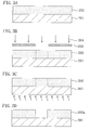
- FIGS. 1A through 1D and 2A through 2D A pattern formation method according to Embodiment 1 of the invention will now be described with reference to FIGS. 1A through 1D and 2A through 2D.
- the aforementioned chemically amplified resist material is applied on a substrate 101 of, for example, silicon oxide so as to form a resist film 102 with a thickness of 0.35 ⁇ m.
- pattern exposure is carried out by irradiating the resist film 102 through a mask 103 with exposing light 104 of ArF excimer laser of a wavelength of 193 nm with NA of 0.68.
- the resist film 102 is baked with a hot plate at a temperature of 105°C for 60 seconds. Thereafter, the resultant resist film 102 is developed with a 0.26 N tetramethylammonium hydroxide developer. In this manner, a resist pattern 102a made of an unexposed portion of the resist film 102 and having an opening width of 0.09 ⁇ m is formed as shown in FIG. 1D.
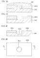
- an acidic aqueous solution 105 including 10 wt% of acrylic acid is dropped onto the resist pattern 102a by what is called a puddle method, thereby exposing the resist pattern 102a to the acidic aqueous solution 105 for 60 seconds.
- lactone rings included in the resist pattern 102a are opened so as to give a resist pattern 102b as shown in FIG 2B .
- FIG. 2C is a cross-sectional view taken on line IIc-IIc of FIG. 2D.
- the resist pattern 102a formed through the development is exposed to the acidic aqueous solution 105 in the step shown in FIG. 2A, the lactone rings included in the resist material are opened before performing the etching. Accordingly, the resist pattern 102b where the lactone rings have been opened is free from surface roughness otherwise caused by the radicals or the like included in the etching gas during the subsequently performed etching (as shown in FIGS. 2C and 2D ). This is for the following reason: Since the lactone rings have been already opened, the radicals used in the etching are never consumed in the ring opening reaction, and therefore, a stable amount of radicals can be supplied to the surface of the substrate 101 to be etched. As a result, the recess 101a formed in the substrate 101 by the etching can be in a good shape.
- a pattern formation method according to Embodiment 2 of the invention will now be described with reference to FIGS. 3A through 3D and 4A through 4D .
- the aforementioned chemically amplified resist material is applied on a substrate 201 of, for example, silicon oxide so as to form a resist film 202 with a thickness of 0.35 ⁇ m.
- pattern exposure is carried out by irradiating the resist film 202 through a mask 203 with exposing light 204 of ArF excimer laser of a wavelength of 193 nm with NA of 0.68.
- the resist film 202 is baked with a hot plate at a temperature of 105°C for 60 seconds. Thereafter, the resultant resist film 202 is developed with a 0.26 N tetramethylammonium hydroxide developer. In this manner, a resist pattern 202a made of an unexposed portion of the resist film 202 and having an opening width of 0.09 ⁇ m is formed as shown in FIG. 3D.
- an alkaline aqueous solution 205 including, for example, 0.30 N of tetramethylammonium hydroxide is dropped onto the resist pattern 202a by what is called a puddle method, thereby exposing the resist pattern 202a to the alkaline aqueous solution 205 for 10 seconds.
- lactone rings included in the resist pattern 202a are opened so as to give a resist pattern 202b as shown in FIG. 4B.
- FIG. 4C is a cross-sectional view taken on line IVc-IVc of FIG. 4D.
- the resist pattern 202a formed through the development is exposed to the alkaline aqueous solution 205 in the step shown in FIG 4A, the lactone rings included in the resist material are opened before performing the etching. Accordingly, the resist pattern 202b where the lactone rings have been opened is free from surface roughness otherwise caused by the radicals or the like included in the etching gas during the subsequently performed etching (as shown in FIGS. 4C and 4D ). This is for the following reason: Since the lactone rings have been already opened, the radicals used in the etching are never consumed in the ring opening reaction, and therefore, a stable amount of radicals can be supplied to the surface of the substrate 201 to be etched. As a result, the recess 201a formed in the substrate 201 by the etching can be in a good shape.
- lactone rings are minimally opened during the development because they are opened at normality approximately 1.1 times as large as the normality of a general alkaline developer, that is, 0.26 N.
- the puddle method is employed for exposing the resist pattern to the acidic or alkaline aqueous solution in Embodiment 1 or 2, which does not limit the invention, and for example, a dip method in which the whole substrate is dipped in a solution may be employed instead.
- ArF excimer laser is used as the exposing light in each embodiment, KrF excimer laser, Xe 2 laser, F 2 laser, KrAr laser or Ar 2 laser may be used instead.
- a fine pattern can be formed in a good shape, and the present invention is useful for forming a fine pattern in fabrication process for semiconductor devices.
Landscapes
- Physics & Mathematics (AREA)
- Spectroscopy & Molecular Physics (AREA)
- General Physics & Mathematics (AREA)
- Materials For Photolithography (AREA)
- Photosensitive Polymer And Photoresist Processing (AREA)
- Exposure Of Semiconductors, Excluding Electron Or Ion Beam Exposure (AREA)
Abstract


Description
- This application claims priority under 35 U.S.C. §119 on Patent Application No. 2005-17818 filed in Japan on January 26, 2005, the entire contents of which are hereby incorporated by reference.
- The present invention relates to a pattern formation method for use in fabrication process or the like for semiconductor devices.
- In accordance with the increased degree of integration of semiconductor integrated circuits and downsizing of semiconductor devices, there are increasing demands for further rapid development of lithography technique. Currently, pattern formation is carried out through photolithography using exposing light of a mercury lamp, KrF excimer laser, ArF excimer laser or the like, and use of F2 laser lasing at a shorter wavelength is being examined. However, since there remain a large number of problems in exposure systems and resist materials, photolithography using exposing light of a shorter wavelength has not been put to practical use.
- In these circumstances, it is regarded significant to increase the life time of ArF excimer laser lithography, and resists for use in the ArF excimer laser lithography are now being developed.
- Some of such ArF resists have a lactone ring in the composition of a polymer included therein (for example, see T. Kudo et al., "Illumination, Acid Diffusion and Process Optimization Considerations for 193 nm Contact Hole Resists", Proc. SPIE, vol. 4690, p. 150 (2002)). This is because a lactone ring is expected to improve the adhesion or the like of a resist pattern onto a target film (i.e., a film to be etched by using the resist pattern).
- Now, a conventional pattern formation method will be described with reference to FIGS. 5A through 5D, 6A and 6B.
- First, a positive chemically amplified resist material having the following composition is prepared:
- Base polymer: poly(2-methyl-2-adamantyl methacrylate (50 mol%) - γ-butyrolactone methacrylate (40 mol%) - 2-hydroxy adamantane methacrylate (10 mol%)) 2 g
- Acid generator: triphenylsulfonium trifluoromethane sulfonate 0.06 g
- Quencher: triethanolamine 0.002 g
- Solvent: propylene glycol monomethyl ether acetate 20 g
- Next, as shown in FIG. 5A, the aforementioned chemically amplified resist material is applied on a
substrate 1 of silicon oxide so as to form aresist film 2 with a thickness of 0.35 µm. - Then, as shown in FIG. 5B, pattern exposure is carried out by irradiating the
resist film 2 with exposinglight 4 of ArF excimer laser of a wavelength of 193 nm with NA of 0.68 through amask 3. - After the pattern exposure, as shown in FIG 5C, the
resist film 2 is baked with a hot plate at a temperature of 105°C for 60 seconds, and the resultant resist film is developed with a 0.26 N tetramethylammonium hydroxide developer. In this manner, aresist pattern 2a made of an unexposed portion of theresist film 2 and having an opening width of 0.09 µm is formed as shown in FIG. 5D. - Next, as shown in FIG 6A, the
substrate 1 is etched with fluorine radicals with theresist pattern 2a used as a mask. At this point, FIG 6A is a cross-sectional view of thesubstrate 1 and FIG. 6B is a plan view of thesubstrate 1 on which theresist pattern 2a is formed. As shown in FIG. 6B, a recess 1a having an opening width of 0.09 µm is formed in thesubstrate 1 through this etching. - However, as shown in FIG. 6B, the recess 1a formed in the
substrate 1 by the conventional pattern formation method is in a defective shape with an irregular wall. - The present inventors have variously examined the reason why the recess 1a formed in the
substrate 1 is in a defective shape, resulting in finding the following: As shown in the cross-sectional view of FIG. 6A and the plan view of FIG. 6B, irregular roughness is caused on the surface of theresist pattern 2a in the etching, and the roughness is transferred to the shape of the recess 1a of thesubstrate 1. Furthermore, the present inventors have found that the surface roughness of theresist pattern 2a is caused because lactone rings, which are included in theresist pattern 2a for improving the adhesion onto thesubstrate 1, are decomposed in the etching. - When such an opening pattern formed in the substrate corresponding to a target film is in a defective shape, the productivity and the yield in the fabrication process for semiconductor devices are disadvantageously lowered.
- In consideration of the aforementioned conventional problem, an object of the invention is preventing the pattern failure caused in a target film in performing etching by using a resist pattern including lactone rings.
- The present inventors have found, on the basis of the results of the aforementioned examination, that surface roughness of a resist pattern caused in etching can be prevented by opening lactone rings included in the resist pattern after forming the resist pattern, namely, before performing the etching.
- Lactone rings heterogeneously open through impact against radicals during the etching. This derives from the structure of a lactone ring. Specifically, a lactone ring has a cyclic structure of a five-membered ring or a six-membered ring including -C(=O)-O- as is well known, and is composed of an aggregate including bonding links with different strengths such as a bonding link between an oxygen atom and a carbon atom and a bonding link between carbon atoms. Specifically, the bonding link between an oxygen atom and a carbon atom has smaller bonding force than the bonding link between carbon atoms. Therefore, the etching resistance of the bonding link between an oxygen atom and a carbon atom is lower than the etching resistance of the bonding link between carbon atoms. Accordingly, the bonding link between an oxygen atom and a carbon atom is more easily opened than the bonding link between carbon atoms through the impact against radicals or the like during the etching. As a result, portions each corresponding to an opened bonding link between an oxygen atom and a carbon atom with low etching resistance are heterogeneously present in the resist pattern, and therefore, the surface of the resist pattern is roughened during the etching.
- Accordingly, if lactone rings included in the resist pattern are opened before the etching, the number of bonding links between carbon atoms in the cyclic portion is reduced, and hence, a difference in the etching resistance in the lactone molecule can be reduced. In other words, a chain compound is produced by previously opening the lactone rings, and hence, the lactone ring can be thus made to have a structure minimally suffering from steric hindrance. As a result, the etching resistance is slightly lowered as a whole and variation in the etching resistance in the resist pattern can be simultaneously reduced, so that the surface roughness otherwise caused in the resist pattern can be prevented.
- In order to open a lactone ring, a resist pattern formed through exposure and development is exposed to an acidic aqueous solution or an alkaline aqueous solution having larger alkali normality than a developer used in the development. Thus, an ester decomposition reaction is caused so as to open a lactone ring. In the case where a lactone ring is opened by using an alkaline aqueous solution, carboxylic acid generated through the opening of the lactone ring is reacted with the alkaline aqueous solution, so that the resist pattern may be disadvantageously dissolved. Therefore, the conditions employed in process for exposing the resist pattern to the alkaline aqueous solution should be carefully set.
- The present invention was devised on the basis of the aforementioned finding, and in the pattern formation method according to the invention in which a lactone ring is included in a resist material, the lactone ring is opened before etching a resist pattern.
- Specifically, the pattern formation method of this invention includes the steps of forming a resist film including a lactone ring on a substrate; performing pattern exposure by selectively irradiating the resist film with exposing light; forming a resist pattern made of the resist film by developing the resist film after the pattern exposure; opening the lactone ring included in the resist pattern; and etching the substrate by using, as a mask, the resist pattern in which the lactone ring has been opened.
- In the pattern formation method of this invention, the lactone ring included in the formed resist pattern is opened before etching the substrate, and therefore, conventional variation that merely a bonding link between an oxygen atom and a carbon atom is opened and a bonding link between carbon atoms is not opened does not occur in the etching. Accordingly, when the resist pattern in which the lactone ring has been opened is used as a mask in etching the substrate, surface roughness of the resist pattern can be prevented, resulting in forming an etching pattern in the substrate in a good shape.
- Although it is preferred that all lactone rings included in the resist pattern are opened, there is no need to always open 100% of lactone rings, and the effect of the invention can be attained when at least approximately 30% of the lactone rings included in the resist pattern are opened.
- In the pattern formation method of the invention, the step of opening the lactone ring is preferably executed by exposing the resist pattern to an acidic aqueous solution. Thus, the lactone ring can be opened through the ester decomposition reaction.
- In this case, the acidic aqueous solution can include a compound having a carboxylic acid group or a sulfonic acid group.
- The compound having a carboxylic acid group can be acrylic acid, methacrylic acid or benzoic acid.
- Also, the compound having a sulfonic acid group can be styrene sulfonic acid.
- Alternatively, in the pattern formation method of the invention, the step of opening the lactone group is preferably executed by exposing the resist pattern to an alkaline aqueous solution having larger alkali normality than a developer used in developing the resist film. Thus, the lactone ring can be opened through the ester decomposition reaction.
- In this case, the alkaline aqueous solution can be an aqueous solution including an amine compound.
- The amine compound can be tetramethylammonium hydroxide, tetraethylammonium hydroxide or choline.
- In the pattern formation method of the invention, the exposing light can be KrF excimer laser, Xe2 laser, ArF excimer laser, F2 laser, KrAr laser or Ar2 laser.
-
- FIGS. 1A, 1B, 1C and 1D are cross-sectional views for showing procedures in a pattern formation method according to
Embodiment 1 of the invention; - FIGS. 2A, 2B and 2C are cross-sectional views for showing other procedures in the pattern formation method of
Embodiment 1 and FIG. 2D is a plan view of FIG. 2C; - FIGS. 3A, 3B, 3C and 3D are cross-sectional views for showing procedures in a pattern formation method according to
Embodiment 2 of the invention; - FIGS. 4A, 4B and 4C are cross-sectional views for showing other procedures in the pattern formation method of
Embodiment 2 and FIG. 4D is a plan view of FIG. 4C; - FIGS. 5A, 5B, 5C and 5D are cross-sectional views for showing procedures in a conventional pattern formation method; and
- FIG. 6A is a cross-sectional view for showing another procedure in the conventional pattern formation method and FIG. 6B is a plan view of FIG. 6A.
- A pattern formation method according to
Embodiment 1 of the invention will now be described with reference to FIGS. 1A through 1D and 2A through 2D. - First, a positive chemically amplified resist material having the following composition is prepared:
- Base polymer: poly(2-methyl-2-adamantyl methacrylate (50 mol%) - γ-butyrolactone methacrylate (40 mol%) - 2-hydroxy admanatane methacrylate (10 mol%)) 2 g
- Acid generator: triphenylsulfonium trifluoromethane sulfonate 0.06 g
- Quencher: triethanolamine 0.002 g
- Solvent: propylene glycol monomethyl ether acetate 20 g
- Next, as shown in FIG. 1A, the aforementioned chemically amplified resist material is applied on a
substrate 101 of, for example, silicon oxide so as to form a resistfilm 102 with a thickness of 0.35 µm. - Then, as shown in FIG. 1B, pattern exposure is carried out by irradiating the resist
film 102 through amask 103 with exposinglight 104 of ArF excimer laser of a wavelength of 193 nm with NA of 0.68. - After the pattern exposure, as shown in FIG. 1C, the resist
film 102 is baked with a hot plate at a temperature of 105°C for 60 seconds. Thereafter, the resultant resistfilm 102 is developed with a 0.26 N tetramethylammonium hydroxide developer. In this manner, a resistpattern 102a made of an unexposed portion of the resistfilm 102 and having an opening width of 0.09 µm is formed as shown in FIG. 1D. - Next, as shown in FIG. 2A, an acidic
aqueous solution 105 including 10 wt% of acrylic acid is dropped onto the resistpattern 102a by what is called a puddle method, thereby exposing the resistpattern 102a to the acidicaqueous solution 105 for 60 seconds. Through this puddle process, lactone rings included in the resistpattern 102a are opened so as to give a resistpattern 102b as shown in FIG 2B. - Then, as shown in FIG. 2C, with the resist
pattern 102b, in which the lactone rings are opened, used as a mask, thesubstrate 101 is etched by using an etching gas including fluorine radicals. In this manner, arecess 101a having an opening width of 0.09 µm is formed in thesubstrate 101 as shown in a plan view of FIG. 2D. At this point, FIG 2C is a cross-sectional view taken on line IIc-IIc of FIG. 2D. - In this manner, according to
Embodiment 1, since the resistpattern 102a formed through the development is exposed to the acidicaqueous solution 105 in the step shown in FIG. 2A, the lactone rings included in the resist material are opened before performing the etching. Accordingly, the resistpattern 102b where the lactone rings have been opened is free from surface roughness otherwise caused by the radicals or the like included in the etching gas during the subsequently performed etching (as shown in FIGS. 2C and 2D). This is for the following reason: Since the lactone rings have been already opened, the radicals used in the etching are never consumed in the ring opening reaction, and therefore, a stable amount of radicals can be supplied to the surface of thesubstrate 101 to be etched. As a result, therecess 101a formed in thesubstrate 101 by the etching can be in a good shape. - A pattern formation method according to
Embodiment 2 of the invention will now be described with reference to FIGS. 3A through 3D and 4A through 4D. - First, a positive chemically amplified resist material having the following composition is prepared:
- Base polymer: poly(2-methyl-2-adamantyl methacrylate (50 mol%) - γ-butyrolactone methacrylate (40 mol%) - 2-hydroxy admanatane methacrylate (10 mol%)) 2 g
- Acid generator: triphenylsulfonium trifluoromethane sulfonate 0.06 g
- Quencher: triethanolamine 0.002 g
- Solvent: propylene glycol monomethyl ether acetate 20 g
- Next, as shown in FIG. 3A, the aforementioned chemically amplified resist material is applied on a
substrate 201 of, for example, silicon oxide so as to form a resistfilm 202 with a thickness of 0.35 µm. - Then, as shown in FIG. 3B, pattern exposure is carried out by irradiating the resist
film 202 through amask 203 with exposinglight 204 of ArF excimer laser of a wavelength of 193 nm with NA of 0.68. - After the pattern exposure, as shown in FIG. 3C, the resist
film 202 is baked with a hot plate at a temperature of 105°C for 60 seconds. Thereafter, the resultant resistfilm 202 is developed with a 0.26 N tetramethylammonium hydroxide developer. In this manner, a resistpattern 202a made of an unexposed portion of the resistfilm 202 and having an opening width of 0.09 µm is formed as shown in FIG. 3D. - Next, as shown in FIG. 4A, an alkaline
aqueous solution 205 including, for example, 0.30 N of tetramethylammonium hydroxide is dropped onto the resistpattern 202a by what is called a puddle method, thereby exposing the resistpattern 202a to the alkalineaqueous solution 205 for 10 seconds. Through this puddle process, lactone rings included in the resistpattern 202a are opened so as to give a resistpattern 202b as shown in FIG. 4B. - Then, as shown in FIG. 4C, with the resist
pattern 202b, in which the lactone rings are opened, used as a mask, thesubstrate 201 is etched by using an etching gas including fluorine radicals. In this manner, arecess 201a having an opening width of 0.09 µm is formed in thesubstrate 201 as shown in a plan view of FIG. 4D. At this point, FIG. 4C is a cross-sectional view taken on line IVc-IVc of FIG. 4D. - In this manner, according to
Embodiment 2, since the resistpattern 202a formed through the development is exposed to the alkalineaqueous solution 205 in the step shown in FIG 4A, the lactone rings included in the resist material are opened before performing the etching. Accordingly, the resistpattern 202b where the lactone rings have been opened is free from surface roughness otherwise caused by the radicals or the like included in the etching gas during the subsequently performed etching (as shown in FIGS. 4C and 4D). This is for the following reason: Since the lactone rings have been already opened, the radicals used in the etching are never consumed in the ring opening reaction, and therefore, a stable amount of radicals can be supplied to the surface of thesubstrate 201 to be etched. As a result, therecess 201a formed in thesubstrate 201 by the etching can be in a good shape. - It is noted that the lactone rings are minimally opened during the development because they are opened at normality approximately 1.1 times as large as the normality of a general alkaline developer, that is, 0.26 N.
- The puddle method is employed for exposing the resist pattern to the acidic or alkaline aqueous solution in
Embodiment - Although a positive chemically amplified resist is used for a resist film in each embodiment, the invention is applicable also to a negative chemically amplified resist.
- Although the ArF excimer laser is used as the exposing light in each embodiment, KrF excimer laser, Xe2 laser, F2 laser, KrAr laser or Ar2 laser may be used instead.
- As described so far, in the pattern formation method of this invention, a fine pattern can be formed in a good shape, and the present invention is useful for forming a fine pattern in fabrication process for semiconductor devices.
Claims (9)
- A pattern formation method comprising the steps of:forming a resist film including a lactone ring on a substrate;performing pattern exposure by selectively irradiating said resist film with exposing light;forming a resist pattern made of said resist film by developing said resist film after the pattern exposure;opening said lactone ring included in said resist pattern; andetching said substrate by using, as a mask, said resist pattern in which said lactone ring has been opened.
- The pattern formation method of Claim 1,
wherein the step of opening said lactone ring is executed by exposing said resist pattern to an acidic aqueous solution. - The pattern formation method of Claim 2,
wherein said acidic aqueous solution includes a compound having a carboxylic acid group or a sulfonic acid group. - The pattern formation method of Claim 3,
wherein said compound having a carboxylic acid group is acrylic acid, methacrylic acid or benzoic acid. - The pattern formation method of Claim 3,
wherein said compound having a sulfonic acid group is styrene sulfonic acid. - The pattern formation method of Claim 1,
wherein the step of opening said lactone group is executed by exposing said resist pattern to an alkaline aqueous solution having larger alkali normality than a developer used in developing said resist film. - The pattern formation method of Claim 6,
wherein said alkaline aqueous solution includes an amine compound. - The pattern formation method of Claim 7,
wherein said amine compound is tetramethylammonium hydroxide, tetraethylammonium hydroxide or choline. - The pattern formation method of Claim 1,
wherein said exposing light is KrF excimer laser, Xe2 laser, ArF excimer laser, F2 laser, KrAr laser or Ar2 laser.
Applications Claiming Priority (1)
| Application Number | Priority Date | Filing Date | Title |
|---|---|---|---|
| JP2005017818A JP4386848B2 (en) | 2005-01-26 | 2005-01-26 | Pattern formation method |
Publications (2)
| Publication Number | Publication Date |
|---|---|
| EP1688797A2 true EP1688797A2 (en) | 2006-08-09 |
| EP1688797A3 EP1688797A3 (en) | 2006-08-16 |
Family
ID=36570774
Family Applications (1)
| Application Number | Title | Priority Date | Filing Date |
|---|---|---|---|
| EP05023540A Withdrawn EP1688797A3 (en) | 2005-01-26 | 2005-10-27 | Pattern formation method |
Country Status (3)
| Country | Link |
|---|---|
| US (1) | US7255974B2 (en) |
| EP (1) | EP1688797A3 (en) |
| JP (1) | JP4386848B2 (en) |
Family Cites Families (3)
| Publication number | Priority date | Publication date | Assignee | Title |
|---|---|---|---|---|
| US6017680A (en) * | 1997-08-05 | 2000-01-25 | Hitachi, Ltd. | Method for pattern formation and process for preparing semiconductor device |
| WO2002044845A2 (en) * | 2000-11-29 | 2002-06-06 | E.I. Du Pont De Nemours And Company | Protecting groups in polymers, photoresists and processes for microlithography |
| JP3853168B2 (en) * | 2001-03-28 | 2006-12-06 | 松下電器産業株式会社 | Pattern formation method |
-
2005
- 2005-01-26 JP JP2005017818A patent/JP4386848B2/en not_active Expired - Lifetime
- 2005-10-27 EP EP05023540A patent/EP1688797A3/en not_active Withdrawn
- 2005-10-28 US US11/260,385 patent/US7255974B2/en not_active Expired - Lifetime
Also Published As
| Publication number | Publication date |
|---|---|
| JP2006208526A (en) | 2006-08-10 |
| EP1688797A3 (en) | 2006-08-16 |
| US7255974B2 (en) | 2007-08-14 |
| US20060163198A1 (en) | 2006-07-27 |
| JP4386848B2 (en) | 2009-12-16 |
Similar Documents
| Publication | Publication Date | Title |
|---|---|---|
| US7541132B2 (en) | Chemically amplified resist material, topcoat film material and pattern formation method using the same | |
| US7132224B2 (en) | Pattern formation method | |
| US7524772B2 (en) | Pattern formation method | |
| US8986918B2 (en) | Hybrid photoresist composition and pattern forming method using thereof | |
| US20050233259A1 (en) | Resist material and pattern formation method using the same | |
| US6908729B2 (en) | Pattern formation method | |
| US7462438B2 (en) | Resist material and pattern formation method using the same | |
| US7338743B2 (en) | Resist material and pattern formation method | |
| US20230384683A1 (en) | Photoresist with polar-acid-labile-group | |
| US7455950B2 (en) | Resist material and pattern formation method using the same | |
| JP4562628B2 (en) | Positive resist composition and pattern forming method using the same | |
| US20050069814A1 (en) | Pattern formation method | |
| US7255974B2 (en) | Pattern formation method | |
| US7029827B2 (en) | Pattern formation method | |
| US6913873B2 (en) | Pattern formation method | |
| JP2004012511A (en) | Pattern formation method | |
| US6936401B2 (en) | Pattern formation material and pattern formation method | |
| JP3152201B2 (en) | Pattern formation method for chemically amplified resist | |
| US20250244664A1 (en) | Photoresist compositions and patterning methods | |
| WO2010113370A1 (en) | Chemically amplified resist material and method for forming pattern using same | |
| US6168909B1 (en) | Material and method for forming pattern | |
| US20040161710A1 (en) | Pattern formation method | |
| KR100269321B1 (en) | Composition of single layer resist for arf | |
| US20060040216A1 (en) | Method of patterning photoresist film | |
| KR100737553B1 (en) | High Sensitivity Resist Composition for Electromagnetic Lithography |
Legal Events
| Date | Code | Title | Description |
|---|---|---|---|
| PUAI | Public reference made under article 153(3) epc to a published international application that has entered the european phase |
Free format text: ORIGINAL CODE: 0009012 |
|
| PUAL | Search report despatched |
Free format text: ORIGINAL CODE: 0009013 |
|
| AK | Designated contracting states |
Kind code of ref document: A2 Designated state(s): AT BE BG CH CY CZ DE DK EE ES FI FR GB GR HU IE IS IT LI LT LU LV MC NL PL PT RO SE SI SK TR |
|
| AX | Request for extension of the european patent |
Extension state: AL BA HR MK YU |
|
| AK | Designated contracting states |
Kind code of ref document: A3 Designated state(s): AT BE BG CH CY CZ DE DK EE ES FI FR GB GR HU IE IS IT LI LT LU LV MC NL PL PT RO SE SI SK TR |
|
| AX | Request for extension of the european patent |
Extension state: AL BA HR MK YU |
|
| RAP1 | Party data changed (applicant data changed or rights of an application transferred) |
Owner name: MATSUSHITA ELECTRIC INDUSTRIAL CO., LTD. |
|
| 17P | Request for examination filed |
Effective date: 20061106 |
|
| 17Q | First examination report despatched |
Effective date: 20070110 |
|
| AKX | Designation fees paid |
Designated state(s): DE FR IT NL |
|
| RBV | Designated contracting states (corrected) |
Designated state(s): DE FR NL |
|
| STAA | Information on the status of an ep patent application or granted ep patent |
Free format text: STATUS: THE APPLICATION HAS BEEN WITHDRAWN |
|
| 18W | Application withdrawn |
Effective date: 20080411 |