EP1684303A1 - Pulse controlled word line driver - Google Patents
Pulse controlled word line driver Download PDFInfo
- Publication number
- EP1684303A1 EP1684303A1 EP05000540A EP05000540A EP1684303A1 EP 1684303 A1 EP1684303 A1 EP 1684303A1 EP 05000540 A EP05000540 A EP 05000540A EP 05000540 A EP05000540 A EP 05000540A EP 1684303 A1 EP1684303 A1 EP 1684303A1
- Authority
- EP
- European Patent Office
- Prior art keywords
- word line
- control signal
- driver
- discharging
- memory
- Prior art date
- Legal status (The legal status is an assumption and is not a legal conclusion. Google has not performed a legal analysis and makes no representation as to the accuracy of the status listed.)
- Granted
Links
- 230000015654 memory Effects 0.000 claims abstract description 107
- 238000007599 discharging Methods 0.000 claims abstract description 56
- 238000000034 method Methods 0.000 claims description 19
- 230000006399 behavior Effects 0.000 claims description 17
- 230000008054 signal transmission Effects 0.000 claims description 12
- 230000009849 deactivation Effects 0.000 claims description 3
- 230000006870 function Effects 0.000 claims description 3
- 230000001960 triggered effect Effects 0.000 claims 1
- 238000010586 diagram Methods 0.000 description 7
- 230000000630 rising effect Effects 0.000 description 6
- 230000004913 activation Effects 0.000 description 4
- 230000008901 benefit Effects 0.000 description 4
- 101100286980 Daucus carota INV2 gene Proteins 0.000 description 3
- 101100397045 Xenopus laevis invs-b gene Proteins 0.000 description 3
- 101150070189 CIN3 gene Proteins 0.000 description 2
- 101150110971 CIN7 gene Proteins 0.000 description 2
- 101100508840 Daucus carota INV3 gene Proteins 0.000 description 2
- 101150110298 INV1 gene Proteins 0.000 description 2
- 101100397044 Xenopus laevis invs-a gene Proteins 0.000 description 2
- 230000003213 activating effect Effects 0.000 description 2
- 230000005540 biological transmission Effects 0.000 description 2
- 230000003071 parasitic effect Effects 0.000 description 2
- 230000007704 transition Effects 0.000 description 2
- 230000008859 change Effects 0.000 description 1
- 238000007796 conventional method Methods 0.000 description 1
- 230000003111 delayed effect Effects 0.000 description 1
- 230000003116 impacting effect Effects 0.000 description 1
- 238000002955 isolation Methods 0.000 description 1
- 230000008569 process Effects 0.000 description 1
- 239000004065 semiconductor Substances 0.000 description 1
- 230000001629 suppression Effects 0.000 description 1
Images


Classifications
-
- G—PHYSICS
- G11—INFORMATION STORAGE
- G11C—STATIC STORES
- G11C11/00—Digital stores characterised by the use of particular electric or magnetic storage elements; Storage elements therefor
- G11C11/21—Digital stores characterised by the use of particular electric or magnetic storage elements; Storage elements therefor using electric elements
- G11C11/34—Digital stores characterised by the use of particular electric or magnetic storage elements; Storage elements therefor using electric elements using semiconductor devices
- G11C11/40—Digital stores characterised by the use of particular electric or magnetic storage elements; Storage elements therefor using electric elements using semiconductor devices using transistors
- G11C11/41—Digital stores characterised by the use of particular electric or magnetic storage elements; Storage elements therefor using electric elements using semiconductor devices using transistors forming static cells with positive feedback, i.e. cells not needing refreshing or charge regeneration, e.g. bistable multivibrator or Schmitt trigger
- G11C11/413—Auxiliary circuits, e.g. for addressing, decoding, driving, writing, sensing, timing or power reduction
-
- G—PHYSICS
- G11—INFORMATION STORAGE
- G11C—STATIC STORES
- G11C8/00—Arrangements for selecting an address in a digital store
- G11C8/08—Word line control circuits, e.g. drivers, boosters, pull-up circuits, pull-down circuits, precharging circuits, for word lines
Definitions
- This capability of the discharging mean can be realised by selecting a discharging transistor with a channel width that is wide enough to conduct an appropriate current through the channel of the discharging transistor.
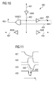
- the pulse 402 obtained after traversing only through the dummy bit line 303 and the pulse 404 obtained after additionally traversing through the dummy word line 302 feed the input terminals of the NAND gate NAND3.
- the NAND gate NAND3 outputs a pulse 405 as shown in Fig. 11.
- arrows 408 and 409 also indicate how the pulse 402 forms the falling edge of the pulse 405 and how the pulse 404 forms the rising edge of the pulse 405.
- the pulse 405 is used to feed the reset terminals RSTB of the row decoders 100 and 200 shown in Fig. 5 and 7. Consequently, the pulses 405 and 104 are identical.
Landscapes
- Engineering & Computer Science (AREA)
- Microelectronics & Electronic Packaging (AREA)
- Computer Hardware Design (AREA)
- Static Random-Access Memory (AREA)
- Read Only Memory (AREA)
Abstract
Description
- The invention relates to driver circuits that drive word lines of memories.
- Until recently a major task in the design of row decoders and their word line drivers was a fast word line activation. But new dynamic and leakage power requirements call for an optimisation of word line drivers in regard to these new constraints. In conventional row decoders the word line deactivation occurs late compared to the ending of a read or a write operation. As a result a lot of power is wasted because of the long time duration the memory cells are opened.
- More recent techniques are able to minimise the word line driver gate leakage current with an automatic suppression device, but they require a local DC level controller, which increases area, adds leakage currents and is not flexible for tuning.
- It is therefore an object of the present invention to provide a word line driver circuit, whose leakage power and in particular whose dynamic power is reduced compared to conventional driver circuits. A memory circuit comprising the word line driver circuit and a method for the same purpose shall be also provided.
- The above formulated object on which the invention is based is achieved by a driver circuit according to
claim 1, a memory circuit according toclaim 10 and a method according to claim 16. - Preferred and advantageous embodiments of the driver circuit according to
claim 1 are subject matter ofclaims 2 to 9. - Preferred and advantageous embodiments of the memory circuit according to
claim 10 are subject matter ofclaim 11 to 15. Preferred and advantageous embodiments of the method according to claim 16 are subject matter of claim 17 to 27. - The driver circuit according to the invention drives a word line of a memory. The memory can be a ROM or an SRAM. The driver circuit comprises a driver unit, a discharging mean and a first signal generator. The driver unit deactivates the word line after an access to a memory cell coupled to the word line. The access to the memory cell can be a read access or a write access. The discharging mean discharges the word line when the word line is deactivated. The first signal generator generates a first control signal and a second control signal. The second control signal follows the first control signal. The first control signal triggers the driver unit to deactivate the word line. Furthermore the first control signal triggers the discharging mean to start discharging the word line. Once the word line is discharged, the second control signal triggers the discharging mean to stop discharging the word line. Keeping the word line at a pre-determined potential is thus not the task of the discharging mean, but rather a task of the driver unit.
- In contrast to conventional driver circuits driving word lines of memories, the driver circuit according to the invention causes the discharging mean to turn off as soon as the word line is discharged. This helps to reduce the overall power consumption of the driver circuit. For example, in case the discharging mean is realised as an MOS transistor, the gate leakage current of this transistor is eliminated after the discharging transistor has discharged the word line. Due to the required width of the discharging transistor the invention helps to reduce the power consumption of the driver circuit significantly.
- Another advantage of the driver circuit according to the invention is that the word line can be deactivated and discharged as soon as the read or write operation is completed. Using a signal from an external signal generator for this purpose allows to deactivate and discharge the word line faster as it can be done by employing word line selection signals for this purpose.
- It can be advantageously be provided that the time period between the first control signal and the second control signal can be controlled. Consequently, the time period during that the discharging mean is activated can be as short as necessary for discharging the word line. Thus the power consumption caused by the discharging mean is reduced as much as possible.
- Instead of generating a first and a second control signal independently, a first pulse can advantageously be generated. The first edge of the first pulse then represents the first signal and the second edge of the first pulse represents the second signal.
- Apart from deactivating the word line, the driver unit also activates the word line when data shall be read from or stored in a memory cell coupled to the word line.
- The driver unit advantageously comprises at least two driver transistors, which are coupled to the word line. The first driver transistor is turned on during an activated period of the word line and for instance connects the word line to a supply voltage. During a deactivated period of the word line the first driver transistor is turned off and a second driver transistor is turned on. During that time the second driver transistor keeps the word line for instance at ground potential.
- Advantageously, the discharging mean comprises a discharging transistor coupled to the word line.
- In accordance with one advantageous configuration of the invention, the word line can be discharged faster by the discharging mean than by the driver unit.
- This capability of the discharging mean can be realised by selecting a discharging transistor with a channel width that is wide enough to conduct an appropriate current through the channel of the discharging transistor.
- The driver transistors are advantageously controlled by the first control signal and not by the second control signal. In contrast to this, the discharging transistor is controlled by the first and the second control signals. This makes it possible to use the first control signal for deactivating the word line and for starting discharging the word line. In contrast to this the second control signal does not reactivate the word line, but only stops discharging the word line.
- The memory circuit according to the invention comprises a plurality a memory cells, which are organised in rows and columns. Word lines are coupled to the rows of memory cells, respectively. Moreover a plurality of driver circuits as described above are coupled to the word lines, respectively.
- Alternatively, it can be provided that the memory circuit comprises only one first signal generator shared by the driver circuits instead of equipping each driver circuit with its own first signal generator.
- Furthermore the memory circuit advantageously comprises a plurality of bit lines, a dummy bit line and a dummy word line. Each bit line is coupled to a column of memory cells. The dummy bit line and the dummy word line are coupled to dummy memory cells. The signal transmission behaviours of the dummy bit line and the dummy word line is essentially characteristic of the signal transmission behaviour of the bit lines and the word lines, respectively.
- In accordance with one advantageous configuration of the invention, the memory circuit contains a second signal generator. The second signal generator generates a third control signal that is supplied to the dummy bit line. The third control signal tracks the height of the memory. The signal outputted by the dummy bit line is used for generating the first control signal. Moreover the signal outputted by the dummy bit line is supplied to the dummy word line. This signal tracks the width of the memory and the load of the word lines. After traversing the dummy word line this signal is used for generating the second control signal.
- The advantage of this concept is that the signals that are responsible for resetting and discharging the word lines are generated by the memory's internal self-timing. This makes it possible to close the memory cells as soon as the read or write operation has been performed. Furthermore, tracking the width of the memory ensures that on the one hand the discharging mean is not turned off before the word line is completely discharged and on the other hand the time period during that the discharging mean is turned on is as short as possible.
- In order to generate the second control signal, it can advantageously be provided that the second signal generator comprises a gate with an AND function. This gate can be implemented for instance as an AND or a NAND gate. The gate is fed with the output signal of the dummy bit line and the output signal of the dummy word line on its input terminals. The output terminal of the gate provides the second control signal and in particular the first control signal.
- A memory circuit usually contains a row decoder that receives row address signals and selects one of the driver circuits according to the row address signals in order to activate the word line coupled to the selected driver circuit. According to the invention, the second signal generator generates the third control signal when the row decoder receives the row address signals. This ensures a minimal cycle time and reduces dynamic power.
- It can be also advantageously provided that the output signal of the dummy bit line caused by the third control signal triggers the reset of a clock DFF. Since most memories are nowadays edge sensitive, a clock DFF is needed to detect the clock signal of the user. When the clock DFF is reset thanks to the internal self-timing of the memory, it is available for the next clock activation. The clock DFF is the central timer of the memory. It controls the pre-charging of the bit lines, the ADD, DIN and RWB latches, the row decoder and the column multiplexer that selects the word and bit lines for a read or write operation.
- The output signal of the dummy bit line also controls a sense amplifier of the memory that is needed in case of a read access to a memory cell. In this case the sense amplifier is coupled to the corresponding bit line.
- In accordance with the present invention, a method of deactivating a word line of a memory is comprised of the following steps:
- (a) Generating a first control signal that triggers the deactivation of the word line after an access to a memory cell coupled to the word line and that triggers a discharging mean to start discharging the word line; and
- (b) Generating a second control signal that triggers the discharging mean to stop discharging the word line.
- The method according to the invention offers the same advantages over conventional methods as the driver circuit according to
claim 1. - The invention is explained below in an exemplary manner with reference to the drawings, in which
- Fig. 1
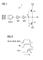
- shows a section of a
conventional row decoder 1 according to prior art; - Fig. 2
- shows diagrams illustrating the behaviour of the word line WL shown in Fig. 1 when selected and when deactivated;
- Fig. 3
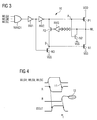
- shows a section of a
conventional row decoder 10 according to prior art; - Fig. 4
- shows diagrams illustrating the behaviour of the word line WL shown in Fig. 3 when selected and when deactivated;
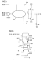
- Fig. 5
- shows a first exemplary embodiment of the driver circuit according to the invention;
- Fig. 6
- shows diagrams illustrating the behaviour of the word line WL shown in Fig. 5 when selected and when deactivated;
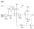
- Fig. 7
- shows a second exemplary embodiment of the driver circuit according to the invention;
- Fig. 8
- shows a memory making use of a dummy bit line according to prior art;
- Fig. 9
- shows a memory making use of a dummy bit line and a dummy word line according to prior art;
- Fig. 10
- shows a
logic circuit 400 used for generating apulse 104; - Fig. 11
- shows diagrams illustrating the signals of the
logic circuit 400 shown in Fig. 10; and - Fig. 12
- shows an exemplary embodiment of the memory circuit according to the invention.
- Fig. 1 shows a section of a
conventional row decoder 1 with a driver circuit according to prior art. The task of therow decoder 1 is to decode row address signals in order to select one word line WL of a ROM or an SRAM. Fig. 1 exemplarily shows only the part of therow decoder 1 that affects a single word line WL. Thus theentire row decoder 1 contains the components shown in Fig. 1 for each word line WL of the memory. - The
row decoder 1 shown in Fig. 1 comprises a NAND gate NAND1, which is fed with word line selection signals WLSA, WLSB and WLSC on its input terminals. The output terminal of the NAND gate NAND1 feeds a serial connection of two inverters INV1 and INV2. The output of the inverter INV2 controls the gate voltages of two transistors N1 and P1. The transistor N1 is a MOS transistor with an n-channel and the transistor P1 is a MOS transistor with a p-channel. Correspondingly, transistors having an n-channel are denoted with an N and transistors having a p-channel are denoted with a P in the following. One channel terminal of each of the transistors N1 and P1 is coupled to a word line WL, whereas the other connections of the transistors N1 and P1 are connected to ground VSS and a supply voltage VDD, respectively. - Fig. 2 illustrates the behaviour of the word line WL in the course of a read or write access to a memory cell coupled to the word line WL. For that, the word line selection signals WLSA, WLSB, WLSC, the potential of the word line WL and an output signal DOUT of the memory are plotted against time t. A change in the output signal DOUT marks the end of a read or write access.
- During a read or write access to a memory cell coupled to the word line WL, the word line selection signals WLSA, WLSB and WSLC are all at a logical high level. This causes the transistor N1 to be switched off and the transistor P1 to be on thus applying the positive supply voltage VDD to the word line WL so that the word line WL is at a logical high level.
- When the read or write access to the memory cell is completed, which is indicated by a transition of the output signal DOUT of the memory from a logical low level to a logical high level, the word line selection signals WLSA, WLSB, WLSC are switched back to the logical low level. Then the potential at a node A, which is the gate potential of the transistors N1 and P1, returns to the logical high level and the word line WL is no longer selected meaning that the potential of the word line WL switches back to the logical low level.
- While the word line WL is not selected, the transistor N1 is always switched on. This results in an increased power consumption of the
row decoder 1 due to a gate leakage current of the transistor N1 as indicated by anarrow 2 in Fig. 1. Since one task of the transistor N1 is to discharge the word line WL after an access to a memory cell, the width of the transistor N1 has to be large enough to fulfil this task. In return the large width of the transistor N1 increases its gate leakage current. In therow decoder 1 the width of the transistor N1 is 10 times larger than a reference value, whereas the width of the transistor P1 is 20 times larger than the reference value. - Another drawback of the
row decoder 1 shown in Fig. 1 and 2 is a long cycle time. The reason for this is that the window during that the word line WL is activated only depends on the word line selection signals WLSA, WLSB and WLSC. The word line selection signals WLSA, WLSB and WLSC come from the address predecoding stage and they are relatively slow because they are generated from the clock DFF. This also becomes evident from Fig. 2. After the output signal DOUT is switched to the logical high level, a lot of time passes by and power is wasted as indicated by an arrow 3, until the word line WL is deactivated. - Fig. 3 shows a section of a further
conventional row decoder 10 with a driver circuit according to prior art. Therow decoder 10 is very similar to therow decoder 1 shown in Fig. 1 except for some additional transistors. Therow decoder 1 comprises a NAND gate NAND1, inverters INV1 and INV2 as well as transistors N1 and P1 that are arranged in almost the same way as in therow decoder 1. However, in contrast to therow decoder 1 the task of the transistor N1 in therow decoder 10 is only to discharge the word line WL in case the word line WL is being deactivated. For this reason the width of the transistor N1 is still 10 times larger than the reference value. (The width of the transistor P1 is 20 times larger than the reference value.) But therow decoder 10 comprises a transistor N2 in order to keep the word line WL at the ground potential VSS when the word line WL is not selected. Since a width of the transistor N2 as large as the reference value is sufficient for keeping the word line WL at the ground potential VSS, the gate leakage current of the transistor N2 is reduced compared to the gate leakage current of the transistor N1 of therow decoder 1 shown in Fig. 1. - Fig. 4 illustrates the behaviour of the word line WL coupled to the
row decoder 10 in the course of a read or write access to a memory cell coupled to the word line WL. For that, the word line selection signals WLSA, WLSB, WLSC, the potentials at nodes A and B as well as the output signal DOUT of the memory are plotted against time t. The potential at the node A is identical to the gate potentials of the transistors P1 and N2, whereas the potential at the node B gives the gate potential of the transistor N1. - Activating the word line WL for a read or write access to a memory cell is performed in the exact same manner as in the
row decoder 1. Since the transistor P2 is on during the read or write access, the gate potentials of the transistors N1 and N2 are at the logical low level during that time and thus switched off. However, when the word line WL shall be deactivated, firstly the potential at the node A is switched to the logical high level as indicated in Fig. 4 by anarrow 11. This causes both transistors N1 and N2 to switch on and the transistor P1 to switch off. Due to its large width the transistor N1 then discharges the word line WL and brings the word line WL to the ground potential VSS. The transistor P2 and a serial connection INV3 of inverters are arranged in such a way that after a certain time determined by the serial connection INV3 of inverters the transistor P2 turns off. Since the transistor N3 is also off, the gate potential of the transistor N1 is then floating which means that its gate is neither connected to the supply voltage VDD nor to the ground potential VSS. However, since the transistor N3 generates a gate leakage current, the potential at the node B, which is also the gate potential of the transistor N1, slowly drops to the logical low level and switches the transistor N1 off. This is indicated in Fig. 4 by acircle 12. During the time needed by the parasitic gate leakage current of the transistor N3 to switch off the transistor N1, the transistor N1 also produces a parasitic gate leakage current, which increases the power consumption of therow decoder 10. - The disadvantages of the
conventional row decoders row decoder 100 that is partially depicted in Fig. 5. Fig. 5 exemplarily shows only the part of therow decoder 100 that affects a single word line WL. Therow decoder 100 comprises a driver circuit and serves as a first exemplary embodiment of the driver circuit according to the invention. - The
row decoder 100 contains a NAND gate NAND1, alogic circuit 101 as well as transistors N1, N2 and P1. Word line selection signals WLSA, WLSB and WLSC feed the input terminals of the NAND gate NAND1. The output terminal of the NAND gate NAND1 and a reset terminal RSTB are connected to input terminals of thelogic circuit 101. Thelogic circuit 101 generates control signals for controlling the transistors N1, N2 and P1 via their gate potentials. The gate terminals of the transistors N2 and P1 are coupled to a node A, whereas the gate terminal of the transistor N1 is coupled to a node B. The arrangement of the transistors N1, N2 and P2 with regard to the word line WL is identical to the arrangement in therow decoder 10 shown in Fig. 3. The widths of the transistors N1 and P1 are 10 and 20 times larger than a reference value, respectively. The width of the transistor N2 is as large as the reference value. - Fig. 6 illustrates the mode of operation of the
row decoder 100 in the course of a read or write access to a memory cell coupled to the word line WL. For that, the word line selection signals WLSA, WLSB, WLSC, the reset signal feeding the reset terminal RSTB, the potentials at the nodes A and B, the potential at the word line WL as well as the output signal DOUT of the memory are plotted against time t. - Activating the word line WL for a read or write access to a memory cell is performed in the exact same manner as in the
row decoders arrows - In order to deactivate the word line WL after the end of a read or write access to a memory cell, a pulse is generated by a control unit, which is not shown in Fig. 5, but will be explained below in more detail. The pulse is induced in the reset terminal RSTB as indicated in Fig. 6 by a dashed
circle 104. When not operated the reset terminal RSTB is at a logical high level. Thus thepulse 104 induced in the reset terminal RSTB comprises a falling edge and a subsequent rising edge. - The falling edge of the
pulse 104 causes the node A to return to the logical high level as indicated by anarrow 105 in Fig. 6. Moreover, the falling edge of thepulse 104 causes the node B to leave the logical low level and to go to the logical high level as indicated by anarrow 106 in Fig. 6. As a result the transistors N1 and N2 are switched on, whereas the transistor P1 is switched off so that the word line WL is discharged by the transistor N1 and is kept at the ground potential VSS by the transistor N2 as indicated by anarrow 107 in Fig. 6. - The falling edge of the
pulse 104 is positioned in such a manner that the word line WL is discharged shortly after the output signal DOUT of the memory has switched from a logical low level to a logical high level. Since this transition of the output signal DOUT is a sign of the completion of the read or write access, only a very short time passes by after the completion of the read or write access until the word line WL is deactivated. Thus the dynamic power is minimised at the end of an operating cycle by optimising the word line window to close the memory cells as soon as the read or write operation is performed. Since thepulse 104 resetting therow decoder 100 is generated from the memory internal self-timing, the memory cells connected to the word line WL can be closed faster than using the slow word line selection signals WLSA, WLSB and WLSC. - Another drawback of the
conventional row decoders row decoder 100, namely the gate leakage current of the transistor N1 used for discharging the word line WL. This is realised by the rising edge of thepulse 104. The rising edge of thepulse 104 causes the node B to return to the logical low level as soon as the word line WL has been discharged. This is marked with anarrow 108 in Fig. 6. As a result the transistor N1 is immediately turned off and cannot produce any gate leakage current any longer. - It is obvious for a person skilled in the art that the
pulse 104 can be also inverted, meaning the rising edge of thepulse 104 is followed by the falling edge. In this case thelogic circuit 101 needs to be adapted to theinverted pulse 104. - In Fig. 7 another
row decoder 200 is shown, which serves as a second exemplary embodiment of the driver circuit according to the invention. Therow decoder 200 is partially identical to therow decoder 100 shown in Fig. 5. The only difference between therow decoders logic circuit 101 in Fig. 7. - In the
row decoder 200 the reset terminal RSTB is connected to the channel terminals of transistors N4 and P3. The other channel terminals of the transistors N4 and P3 are connected to a first input terminal of a NAND gate NAND2 and to the input terminal of an inverter INV5. The gate of the transistor P3 is controlled by the output signal of the NAND gate NAND1, whereas the output signal of the NAND gate NAND1 is inverted by an inverter INV4 before it is supplied to the gate terminal of the transistor N4. The output signal of the inverter INV4 also feeds the second input terminal of the NAND gate NAND2 and controls the gate of a transistor P5, the channel of which is inserted between the supply voltage VDD and the first input terminal of the NAND gate NAND2. The output terminals of the NAND gate NAND2 and the inverter INV5 form the nodes A and B, respectively. - The circuit arrangement of the
logic circuit 101 as shown in Fig. 7 functions as illustrated in Fig. 6. The components of thelogic circuit 101 shown in Fig. 7 are arranged in such a way that the falling edge of thepulse 104 affects both the node A and the node B. However, the rising edge of thepulse 104 only affects the node B. - An additional benefit of the
row decoder 200 is the ability to select the word line WL faster thanks to a reduced gate load on the word line activation critical path, because the gate of the transistor N1 is no longer on this path. As the word line driver input load is reduced, it gives more flexibility to increase the length of the transistor P1 to reduce the sub-threshold leakage current without impacting too much the access time. - The width of the
pulse 104 is not controlled locally in therow decoder 200 meaning that no additional control logic is needed in therow decoder 200. Thepulse 104 is rather derived from the internal-self timing of the memory. One approach for generating thepulse 104 and especially for controlling its width makes use of the so-called double dummy line concept. - Generally, a dummy line replicates a corresponding word line or bit line. For that the dummy line is connected to a number of dummy transistors. The number of the dummy transistors is the same as the number of transistors connected to the corresponding word line or bit line. Furthermore, the dummy line and the corresponding word line or bit line are matched to each other. Matching between these two lines means that the main characteristic structure features of both transmission lines, which impacts the line capacitance and the propagation delay of the transmission line, are identical, e.g. same length, same width, same thickness and same dielectricity of the isolation. Then the signal transmission behaviour of the dummy line is essentially characteristic of the signal transmission behaviour of the corresponding word line or bit line. For example, if the delay for reading the content of a memory cell via a bit line is increased, e.g. caused by semiconductor process variations, the dummy bit line reflects this delay. Then the activation of a sense amplifier can be also delayed by the same additional delay. This leads to a self-adjusting timing architecture.
- Fig. 8 and 9 show schematically the internal arrangement of a conventional SRAM or
ROM 300 according to prior art. Thememory 300 comprises an array ofmemory cells 301 organised in n+1 rows and n-1-n/2 columns. Eachmemory cell 301 is addressed by a row address signal and a column address signal. The row address signal is decoded in a row decoder to select one of the n+1 rows. In Fig. 8 and 9 the row decoder is composed of several sections denoted asrowdec 0 to rowdec n. Eachsection rowdec 0 to rowdec n of the row decoder drives one of the word lines WL. Every section rowdec 0 to rowdec n for example corresponds to the section of therow decoder 10 shown in Fig. 3. Each row ofmemory cells 301 is coupled to one of the word lines. In case a row is selected the corresponding word line exhibits a logical high level. In a similar way, the column address signal is decoded in a column decoder to select one of the n-1-n/2 columns. Each column ofmemory cells 301 is coupled to one of the bit lines. - Furthermore the
memory 300 comprises adummy word line 302 and adummy bit line 303. Thedummy word line 302 is connected to n+1dummy memory cells 304, whereas thedummy bit line 303 is connected to n-1-n/2dummy memory cells 304. Thedummy cells 304 are identical to thememory cells 301. - In Fig. 8 only the
dummy bit line 303 is used for tracking the height of thememory 300. The voltage level of thedummy bit line 303 is used for resetting the clock DFF and for triggering the sense amplifier of thememory 300 in case of a read access. - In Fig. 9 both the
dummy word line 302 and thedummy bit line 303 are used for tracking the width and the height of thememory 300. - In Fig. 10 a
logic circuit 400 is shown that generates thepulse 104 shown in Fig. 6 by making use of dummy word and dummy bit lines in order to reset the word lines WL driven by therow decoders logic circuit 400 comprises inverters INV6, INV7, INV8 and INV9 as well as a NAND gate NAND3. The inverter INV6 is fed with asignal 401 on its input terminal and produces asignal 402 on its output terminal. The output terminal of the inverter INV6 is connected to the input terminals of the inverters INV7, INV8 as well as INV9 and is also connected to the first input terminal of the NAND gate NAND3. The second input terminal of the NAND gate NAND3 is fed with asignal 404. On the output terminals of the NAND gate NAND3 and the inverters INV7, INV8 and INV9 signals 405, 403, 406 and 407 are respectively generated. - Fig. 11 illustrates the mode of operation of the
logic circuit 400. In Fig. 11 thesignals - Fig. 12 shows the implementation of the
logic circuit 400 in an SRAM or aROM 500. Thememory 500 serves as an exemplary embodiment of the memory circuit according to the invention. Most parts of thememory 500 are identical to thememories 300 shown in Fig. 8 and 9. The corresponding components in Fig. 12 are denoted with the same reference signs. The sections rowdec 0 to rowdec n of thememory 500 correspond to the circuit diagrams shown in Fig. 5 and 7. - In order to generate the
pulse 104, firstly a pulse is generated that is supplied to thedummy bit line 303. This pulse is generated by a section rowdec dummy of therow decoder dummy word line 302. The circuit diagram of the section rowdec dummy is identical to one of the circuit diagrams shown in Fig. 5 and 7. In fact the pulse feeding thedummy bit line 303 is generated when all three word line selection signals WLSA, WLSB and WLSC feeding any of the sections rowdec 0 to rowdec n become 1. At this moment the section rowdec dummy connected to thedummy word line 302 creates a pulse. In other words this means that every time a word line WL is selected by its word line selection signals WLSA, WLSB and WLSC, the section rowdec dummy creates a pulse that is supplied to thedummy bit line 303. - After passing the
dummy bit line 303 thepulse 401 is obtained on the output terminal of thedummy bit line 303. As shown in Fig. 10 thesignals pulse 401. Thesignal 406 triggers the sense amplifier of the memory in case of a read access to thememory 500 and thesignal 407 resets the clock DFF. Moreover thepulse 403 is obtained from thepulse 401. Thepulse 403 feeds thedummy word line 302 at its input terminal. After passing thedummy word line 302 thepulse 404 is obtained at the output terminal of thedummy word line 302. - The
pulse 402 obtained after traversing only through thedummy bit line 303 and thepulse 404 obtained after additionally traversing through thedummy word line 302 feed the input terminals of the NAND gate NAND3. As a result the NAND gate NAND3 outputs apulse 405 as shown in Fig. 11. In Fig. 11arrows pulse 402 forms the falling edge of thepulse 405 and how thepulse 404 forms the rising edge of thepulse 405. Finally thepulse 405 is used to feed the reset terminals RSTB of therow decoders pulses - It can be provided that the
pulse 405 is not only supplied to the section of therow decoder pulse 405 is supplied to all sections rowdec 0 to rowdec n. - The
memory 500 is advantageous over theconventional memory 300 because thepulse 104, which resets and discharges the word lines WL, is generated by the memory's internal self-timing. Tracking the height of thememory 500 by employing thedummy bit line 303 makes it possible to close thememory cells 301 as soon as the read or write operation has been performed. Furthermore, tracking the width of thememory 500 by using thedummy word line 302 ensures that on the one hand the discharging transistor N1 is not turned off before the word line WL is completely discharged and on the other hand the time period during that the discharging transistor N1 is turned on is as short as possible.
Claims (27)
- A driver circuit (100; 200) for driving a word line (WL) of a memory (500), comprising:- a driver unit (N2, P1) for deactivating the word line (WL) after an access to a memory cell (301) coupled to the word line (WL),- a discharging mean (N1) for discharging the word line (WL), and- a first signal generator (101) that is designed to generate a first control signal and a subsequent second control signal, with the first control signal triggering the driver unit (N2, P1) to deactivate the word line (WL) and the first control signal triggering the discharging mean (N1) to start discharging the word line (WL) and the second control signal triggering the discharging mean (N1) to stop discharging the word line (WL).
- The driver circuit (100; 200) according to claim 1,
characterised in that- the time period between the first control signal and the second control signal is controllable. - The driver circuit (100; 200) according to claim 1 or according to claim 2,
characterised in that- the first signal generator (101) is designed to generate a first pulse (104), with the first edge of the first pulse (104) being the first control signal and the second edge of the first pulse (104) being the second control signal. - The driver circuit (100; 200) according to one or more of the preceding claims,
characterised in that- the driver unit (N2, P1) is also designed to activate the word line (WL) before an access to a memory cell (301) coupled to the word line (WL). - The driver circuit (100; 200) according to one or more of the preceding claims,
characterised in that- the driver unit comprises at least two driver transistors (P1, N2) coupled to the word line (WL), with the first driver transistor (P1) being switched on during an activated period of the word line (WL) and the second driver transistor (N2) being switched on during an deactivated period of the word line (WL). - The driver circuit (100; 200) according to one or more of the preceding claims,
characterised in that- the discharging mean comprises a discharging transistor (N1) coupled to the word line (WL). - The driver circuit (100; 200) according to one or more of the preceding claims,
characterised in that- the discharging mean (N1) is able to discharge the word line (WL) faster than the driver unit (N2, P1). - The driver circuit (100; 200) according to claims 5 and 7,
characterised in that- the channel width of the discharging transistor (N1) is larger than the channel width of the second driver transistor (N2). - The driver circuit (100; 200) according to one or more of the claims 5 to 8,
characterised in that- the driver transistors (N2, P1) are controlled by the first control signal and not by the second control signal, and- the discharging transistor (N1) is controlled by the first and the second control signal. - A memory circuit (500) comprising:- a plurality a memory cells (301) organised in rows and columns,- a plurality of word lines (WL) each coupled to a row of memory cells (301), and- a plurality of driver circuits (100; 200) according to one or more of the preceding claims, each coupled to a word line (WL).
- The memory circuit (500) according to claim 10,
characterised in that- the memory circuit (500) comprises- a plurality of bit lines each coupled to a column of memory cells (301),- a dummy bit line (303), the signal transmission behaviour of which is essentially characteristic of the signal transmission behaviour of the bit lines, and- a dummy word line (302), the signal transmission behaviour of which is essentially characteristic of the signal transmission behaviour of the word lines (WL). - The memory circuit (500) according to claim 10 or to claim 11,
characterised in that- the memory circuit (500) comprises a second signal generator (400) feeding the dummy bit line (303) with a third control signal and feeding the dummy word line (302) with the output signal (403) of the dummy bit line (303), with using the output signal (402) of the dummy bit line (303) for triggering the first signal generator (101) of at least one driver circuit (100; 200) to generate the first control signal and using the output signal (404) of the dummy word line (302) for triggering the first signal generator (101) of the at least one driver circuit (100; 200) to generate the second control signal. - The memory circuit (500) according to claim 12,
characterised in that- the second signal generator (400) comprises a gate (NAND3) with an AND function that is fed with the output signal (402) of the dummy bit line (303) and the output signal (404) of the dummy word line (302) on its input terminals and whose output signal triggers the first signal generator (101) of the at least one driver circuit (100; 200) to generate the first and the second control signals. - The memory circuit (500) according to one or more of the claims 10 to 13,
characterised in that- the memory circuit (500) comprises a row decoder (rowdec 0,..., rowdec n, rowdec dummy) that receives row address signals and selects one of the driver circuits (100; 200) according to the row address signals in order to activate the word line (WL) coupled to the selected driver circuit (100; 200), and- the generation of the third control signal by the second signal generator (400) is triggered by the point in time the row decoder (rowdec 0,..., rowdec n, rowdec dummy) receives the row address signals. - The memory circuit (500) according to one or more of the claims 10 to 14,
characterised in that- the output signal (402) of the dummy bit line (303) triggers the reset of a clock DFF and controls a sense amplifier for a memory read access, with the sense amplifier being selectively coupled to one of the bit lines. - A method of deactivating a word line (WL) of a memory (500) comprised of the following steps:(a) Generating a first control signal that triggers the deactivation of the word line (WL) after an access to a memory cell (301) coupled to the word line (WL) and that triggers a discharging mean (N1) to start discharging the word line (WL); and(b) Generating a second control signal that triggers the discharging mean (N1) to stop discharging the word line (WL).
- The method according to claim 16,
characterised in that- the time period between the first control signal and the second control signal is controllable. - The method according to claim 16 or according to claim 17,
characterised in that- a first pulse (104) is generated, with the first edge of the first pulse (104) being the first control signal and the second edge of the first pulse (104) being the second control signal. - The method according to one or more of the claims 16 to 18,
characterised in that- the word line (WL) is activated before an access to a memory cell (301) coupled to the word line (WL). - The method according to one or more of the claims 16 to 19,
characterised in that- a first driver transistor (P1) coupled to the word line (WL) is switched on during an activated period of the word line (WL) and a second driver transistor (N2) coupled to the word line (WL) is switched on during an deactivated period of the word line (WL). - The method according to one or more of the claims 16 to 20,
characterised in that- a discharging transistor (N1) discharges the word line (WL). - The method according to claims 20 and 21,
characterised in that- the channel width of the discharging transistor (N1) is larger than the channel width of the second driver transistor (N2). - The method according to claims 20 to 22,
characterised in that- the driver transistors (N2, P1) are controlled by the first control signal and not by the second control signal, and- the discharging transistor (N1) is controlled by the first and the second control signal. - The method according to one or more of the claims 16 to 23,
characterised in that- the word line (WL) is a word line of a memory circuit (500) that comprises a plurality a memory cells (301) organised in rows and columns and a plurality of word lines (WL) each coupled to a row of memory cells (301). - The method according to claim 24,
characterised in that- the memory circuit (500) comprises- a plurality of bit lines each coupled to a column of memory cells (301),- a dummy bit line (303), the signal transmission behaviour of which is essentially characteristic of the signal transmission behaviour of the bit lines, and- a dummy word line (302), the signal transmission behaviour of which is essentially characteristic of the signal transmission behaviour of the word lines (WL). - The method according to claim 25,
characterised in that- a third control signal is generated that feeds the dummy bit line (303),- the output signal (403) of the dummy bit line (303) feeds the dummy word line (302),- the output signal (402) of the dummy bit line (303) triggers the generation of the first control signal, and- the output signal (404) of the dummy word line (302) triggers the generation of the second control signal. - The method according to claim 26,
characterised in that- the output signal (402) of the dummy bit line (303) triggers the reset of a clock DFF and controls a sense amplifier for a memory read access, with the sense amplifier being selectively coupled to one of the bit lines.
Priority Applications (3)
| Application Number | Priority Date | Filing Date | Title |
|---|---|---|---|
| EP05000540A EP1684303B1 (en) | 2005-01-12 | 2005-01-12 | Pulse controlled word line driver |
| DE602005020414T DE602005020414D1 (en) | 2005-01-12 | 2005-01-12 | Pulse-controlled word line driver |
| US11/331,408 US7403442B2 (en) | 2005-01-12 | 2006-01-12 | Pulse controlled word line driver |
Applications Claiming Priority (1)
| Application Number | Priority Date | Filing Date | Title |
|---|---|---|---|
| EP05000540A EP1684303B1 (en) | 2005-01-12 | 2005-01-12 | Pulse controlled word line driver |
Publications (2)
| Publication Number | Publication Date |
|---|---|
| EP1684303A1 true EP1684303A1 (en) | 2006-07-26 |
| EP1684303B1 EP1684303B1 (en) | 2010-04-07 |
Family
ID=34933270
Family Applications (1)
| Application Number | Title | Priority Date | Filing Date |
|---|---|---|---|
| EP05000540A Ceased EP1684303B1 (en) | 2005-01-12 | 2005-01-12 | Pulse controlled word line driver |
Country Status (3)
| Country | Link |
|---|---|
| US (1) | US7403442B2 (en) |
| EP (1) | EP1684303B1 (en) |
| DE (1) | DE602005020414D1 (en) |
Families Citing this family (12)
| Publication number | Priority date | Publication date | Assignee | Title |
|---|---|---|---|---|
| JP4962828B2 (en) * | 2004-08-25 | 2012-06-27 | マイクロン テクノロジー, インク. | Word line driver circuit and method of using the same |
| JP4850661B2 (en) * | 2006-10-31 | 2012-01-11 | 富士通セミコンダクター株式会社 | Semiconductor memory device |
| US7532513B2 (en) * | 2007-08-27 | 2009-05-12 | Macronix International Co., Ltd. | Apparatus and method for detecting word line leakage in memory devices |
| US10103317B2 (en) | 2015-01-05 | 2018-10-16 | Inston, Inc. | Systems and methods for implementing efficient magnetoelectric junctions |
| US10217798B2 (en) | 2015-01-13 | 2019-02-26 | Inston, Inc. | Systems and methods for implementing select devices constructed from 2D materials |
| US9978931B2 (en) | 2015-02-13 | 2018-05-22 | Inston Inc. | Systems and methods for implementing robust magnetoelectric junctions |
| US10102893B2 (en) | 2016-06-28 | 2018-10-16 | Inston Inc. | Systems for implementing word line pulse techniques in magnetoelectric junctions |
| CN108389860B (en) * | 2017-02-03 | 2021-06-22 | 联华电子股份有限公司 | semiconductor device |
| US10658026B2 (en) * | 2017-05-26 | 2020-05-19 | Taiwan Semiconductor Manufacturing Company Limited | Word line pulse width control circuit in static random access memory |
| US10861527B2 (en) | 2017-06-27 | 2020-12-08 | Inston, Inc. | Systems and methods for optimizing magnetic torque and pulse shaping for reducing write error rate in magnetoelectric random access memory |
| US10460786B2 (en) | 2017-06-27 | 2019-10-29 | Inston, Inc. | Systems and methods for reducing write error rate in magnetoelectric random access memory through pulse sharpening and reverse pulse schemes |
| WO2021232233A1 (en) * | 2020-05-19 | 2021-11-25 | Yangtze Memory Technologies Co., Ltd. | Control method and controller of program suspending and resuming for memory |
Citations (6)
| Publication number | Priority date | Publication date | Assignee | Title |
|---|---|---|---|---|
| US4516224A (en) * | 1981-07-29 | 1985-05-07 | Fujitsu Limited | Semiconductor memory |
| US5719818A (en) * | 1996-04-18 | 1998-02-17 | Waferscale Integration Inc. | Row decoder having triple transistor word line drivers |
| US20020141278A1 (en) * | 2001-04-02 | 2002-10-03 | Peter Weitz | Circuit configuration for controlling the word lines of a memory matrix |
| EP1255254A2 (en) * | 2001-05-04 | 2002-11-06 | Samsung Electronics Co., Ltd. | Word line driver for a semiconductor memory device |
| US20030206448A1 (en) * | 2002-05-03 | 2003-11-06 | Sung Nak-Woo | Sense amplifier enable signal generating circuits having process tracking capability and semiconductor memory devices including the same |
| US6646949B1 (en) * | 2000-03-29 | 2003-11-11 | International Business Machines Corporation | Word line driver for dynamic random access memories |
Family Cites Families (4)
| Publication number | Priority date | Publication date | Assignee | Title |
|---|---|---|---|---|
| US6278297B1 (en) * | 1999-09-14 | 2001-08-21 | Texas Instruments Incorporated | Row decoder with switched power supply |
| KR100454259B1 (en) * | 2001-11-02 | 2004-10-26 | 주식회사 하이닉스반도체 | Semiconductor Memor Device having a Monitoring Circuit |
| JP2003242787A (en) * | 2002-02-14 | 2003-08-29 | Mitsubishi Electric Corp | Nonvolatile semiconductor memory device |
| JP4167458B2 (en) * | 2002-07-24 | 2008-10-15 | 松下電器産業株式会社 | Semiconductor memory device and semiconductor integrated circuit |
-
2005
- 2005-01-12 DE DE602005020414T patent/DE602005020414D1/en not_active Expired - Lifetime
- 2005-01-12 EP EP05000540A patent/EP1684303B1/en not_active Ceased
-
2006
- 2006-01-12 US US11/331,408 patent/US7403442B2/en not_active Expired - Fee Related
Patent Citations (6)
| Publication number | Priority date | Publication date | Assignee | Title |
|---|---|---|---|---|
| US4516224A (en) * | 1981-07-29 | 1985-05-07 | Fujitsu Limited | Semiconductor memory |
| US5719818A (en) * | 1996-04-18 | 1998-02-17 | Waferscale Integration Inc. | Row decoder having triple transistor word line drivers |
| US6646949B1 (en) * | 2000-03-29 | 2003-11-11 | International Business Machines Corporation | Word line driver for dynamic random access memories |
| US20020141278A1 (en) * | 2001-04-02 | 2002-10-03 | Peter Weitz | Circuit configuration for controlling the word lines of a memory matrix |
| EP1255254A2 (en) * | 2001-05-04 | 2002-11-06 | Samsung Electronics Co., Ltd. | Word line driver for a semiconductor memory device |
| US20030206448A1 (en) * | 2002-05-03 | 2003-11-06 | Sung Nak-Woo | Sense amplifier enable signal generating circuits having process tracking capability and semiconductor memory devices including the same |
Also Published As
| Publication number | Publication date |
|---|---|
| DE602005020414D1 (en) | 2010-05-20 |
| EP1684303B1 (en) | 2010-04-07 |
| US20060198231A1 (en) | 2006-09-07 |
| US7403442B2 (en) | 2008-07-22 |
Similar Documents
| Publication | Publication Date | Title |
|---|---|---|
| US8233342B2 (en) | Apparatus and method for implementing write assist for static random access memory arrays | |
| EP0649146B1 (en) | Semiconductor integrated circuit device | |
| JPH0652685A (en) | Semiconductor memory having power-on reset- control latch type line repeater | |
| US20120008438A1 (en) | Efficient word lines, bit line and precharge tracking in self-timed memory device | |
| US20040004899A1 (en) | Word line driving circuit | |
| JP2000057766A (en) | Boost voltage drive circuit and semiconductor memory device using the same | |
| JP2007323808A (en) | X decoder for semiconductor memory device | |
| EP1684303B1 (en) | Pulse controlled word line driver | |
| US6031781A (en) | Semiconductor memory device allowing high-speed activation of internal circuit | |
| KR100349481B1 (en) | Semiconductor memory device | |
| US7982505B2 (en) | Logic circuit, address decoder circuit and semiconductor memory | |
| JP3259764B2 (en) | Semiconductor storage device | |
| JPH09231767A (en) | Static semiconductor memory device | |
| KR20000062709A (en) | Word-line driving circuit and semiconductor memory device | |
| US6272057B1 (en) | Semiconductor memory device | |
| US6480431B2 (en) | Semiconductor having mechanism capable of operating at high speed | |
| US5640365A (en) | Semiconductor memory device with a decoding peripheral circuit for improving the operation frequency | |
| JP4562515B2 (en) | Logic circuit and word driver circuit | |
| US6825704B2 (en) | Pulse generation circuit enabling its output pulse cycle to be shortened | |
| US8854902B2 (en) | Write self timing circuitry for self-timed memory | |
| US6990011B2 (en) | Memory circuit and method for corrupting stored data | |
| KR101556016B1 (en) | A semiconductor memory device having a power saving mode | |
| JPH08293198A (en) | Semiconductor memory | |
| US7196964B2 (en) | Selectable memory word line deactivation | |
| US6580656B2 (en) | Semiconductor memory device having memory cell block activation control circuit and method for controlling activation of memory cell blocks thereof |
Legal Events
| Date | Code | Title | Description |
|---|---|---|---|
| PUAI | Public reference made under article 153(3) epc to a published international application that has entered the european phase |
Free format text: ORIGINAL CODE: 0009012 |
|
| AK | Designated contracting states |
Kind code of ref document: A1 Designated state(s): AT BE BG CH CY CZ DE DK EE ES FI FR GB GR HU IE IS IT LI LT LU MC NL PL PT RO SE SI SK TR |
|
| AX | Request for extension of the european patent |
Extension state: AL BA HR LV MK YU |
|
| 17P | Request for examination filed |
Effective date: 20061130 |
|
| 17Q | First examination report despatched |
Effective date: 20070119 |
|
| AKX | Designation fees paid |
Designated state(s): DE FR GB |
|
| GRAP | Despatch of communication of intention to grant a patent |
Free format text: ORIGINAL CODE: EPIDOSNIGR1 |
|
| GRAC | Information related to communication of intention to grant a patent modified |
Free format text: ORIGINAL CODE: EPIDOSCIGR1 |
|
| GRAS | Grant fee paid |
Free format text: ORIGINAL CODE: EPIDOSNIGR3 |
|
| GRAA | (expected) grant |
Free format text: ORIGINAL CODE: 0009210 |
|
| AK | Designated contracting states |
Kind code of ref document: B1 Designated state(s): DE FR GB |
|
| REG | Reference to a national code |
Ref country code: GB Ref legal event code: FG4D |
|
| REF | Corresponds to: |
Ref document number: 602005020414 Country of ref document: DE Date of ref document: 20100520 Kind code of ref document: P |
|
| RAP2 | Party data changed (patent owner data changed or rights of a patent transferred) |
Owner name: INFINEON TECHNOLOGIES AG |
|
| REG | Reference to a national code |
Ref country code: FR Ref legal event code: CA |
|
| PLBE | No opposition filed within time limit |
Free format text: ORIGINAL CODE: 0009261 |
|
| STAA | Information on the status of an ep patent application or granted ep patent |
Free format text: STATUS: NO OPPOSITION FILED WITHIN TIME LIMIT |
|
| 26N | No opposition filed |
Effective date: 20110110 |
|
| REG | Reference to a national code |
Ref country code: FR Ref legal event code: PLFP Year of fee payment: 12 |
|
| REG | Reference to a national code |
Ref country code: FR Ref legal event code: PLFP Year of fee payment: 13 |
|
| REG | Reference to a national code |
Ref country code: FR Ref legal event code: PLFP Year of fee payment: 14 |
|
| PGFP | Annual fee paid to national office [announced via postgrant information from national office to epo] |
Ref country code: FR Payment date: 20190123 Year of fee payment: 15 Ref country code: GB Payment date: 20190121 Year of fee payment: 15 |
|
| PGFP | Annual fee paid to national office [announced via postgrant information from national office to epo] |
Ref country code: DE Payment date: 20190321 Year of fee payment: 15 |
|
| REG | Reference to a national code |
Ref country code: DE Ref legal event code: R119 Ref document number: 602005020414 Country of ref document: DE |
|
| GBPC | Gb: european patent ceased through non-payment of renewal fee |
Effective date: 20200112 |
|
| PG25 | Lapsed in a contracting state [announced via postgrant information from national office to epo] |
Ref country code: FR Free format text: LAPSE BECAUSE OF NON-PAYMENT OF DUE FEES Effective date: 20200131 Ref country code: DE Free format text: LAPSE BECAUSE OF NON-PAYMENT OF DUE FEES Effective date: 20200801 Ref country code: GB Free format text: LAPSE BECAUSE OF NON-PAYMENT OF DUE FEES Effective date: 20200112 |