EP1681724A2 - CMOS active pixel sensor with improved dark current and sensitivity - Google Patents
CMOS active pixel sensor with improved dark current and sensitivity Download PDFInfo
- Publication number
- EP1681724A2 EP1681724A2 EP06392001A EP06392001A EP1681724A2 EP 1681724 A2 EP1681724 A2 EP 1681724A2 EP 06392001 A EP06392001 A EP 06392001A EP 06392001 A EP06392001 A EP 06392001A EP 1681724 A2 EP1681724 A2 EP 1681724A2
- Authority
- EP
- European Patent Office
- Prior art keywords
- well
- region
- active pixel
- pixel sensor
- gate electrode
- Prior art date
- Legal status (The legal status is an assumption and is not a legal conclusion. Google has not performed a legal analysis and makes no representation as to the accuracy of the status listed.)
- Withdrawn
Links
Images

Classifications
-
- H—ELECTRICITY
- H10—SEMICONDUCTOR DEVICES; ELECTRIC SOLID-STATE DEVICES NOT OTHERWISE PROVIDED FOR
- H10F—INORGANIC SEMICONDUCTOR DEVICES SENSITIVE TO INFRARED RADIATION, LIGHT, ELECTROMAGNETIC RADIATION OF SHORTER WAVELENGTH OR CORPUSCULAR RADIATION
- H10F39/00—Integrated devices, or assemblies of multiple devices, comprising at least one element covered by group H10F30/00, e.g. radiation detectors comprising photodiode arrays
- H10F39/80—Constructional details of image sensors
- H10F39/802—Geometry or disposition of elements in pixels, e.g. address-lines or gate electrodes
-
- H—ELECTRICITY
- H10—SEMICONDUCTOR DEVICES; ELECTRIC SOLID-STATE DEVICES NOT OTHERWISE PROVIDED FOR
- H10F—INORGANIC SEMICONDUCTOR DEVICES SENSITIVE TO INFRARED RADIATION, LIGHT, ELECTROMAGNETIC RADIATION OF SHORTER WAVELENGTH OR CORPUSCULAR RADIATION
- H10F39/00—Integrated devices, or assemblies of multiple devices, comprising at least one element covered by group H10F30/00, e.g. radiation detectors comprising photodiode arrays
- H10F39/10—Integrated devices
- H10F39/12—Image sensors
- H10F39/18—Complementary metal-oxide-semiconductor [CMOS] image sensors; Photodiode array image sensors
-
- H—ELECTRICITY
- H10—SEMICONDUCTOR DEVICES; ELECTRIC SOLID-STATE DEVICES NOT OTHERWISE PROVIDED FOR
- H10F—INORGANIC SEMICONDUCTOR DEVICES SENSITIVE TO INFRARED RADIATION, LIGHT, ELECTROMAGNETIC RADIATION OF SHORTER WAVELENGTH OR CORPUSCULAR RADIATION
- H10F39/00—Integrated devices, or assemblies of multiple devices, comprising at least one element covered by group H10F30/00, e.g. radiation detectors comprising photodiode arrays
- H10F39/80—Constructional details of image sensors
- H10F39/803—Pixels having integrated switching, control, storage or amplification elements
-
- H—ELECTRICITY
- H10—SEMICONDUCTOR DEVICES; ELECTRIC SOLID-STATE DEVICES NOT OTHERWISE PROVIDED FOR
- H10F—INORGANIC SEMICONDUCTOR DEVICES SENSITIVE TO INFRARED RADIATION, LIGHT, ELECTROMAGNETIC RADIATION OF SHORTER WAVELENGTH OR CORPUSCULAR RADIATION
- H10F39/00—Integrated devices, or assemblies of multiple devices, comprising at least one element covered by group H10F30/00, e.g. radiation detectors comprising photodiode arrays
- H10F39/80—Constructional details of image sensors
- H10F39/807—Pixel isolation structures
Definitions
- This invention relates to an active pixel sensor fabricated using standard CMOS processing and more particularly to dark current suppression and improved sensitivity in active pixel sensors fabricated using standard CMOS processing.
- U.S. Pat. No. 6,649,950 B2 to He et al. describes substantially covering the surface of a photodiode structure in order to reduce dark current due to surface damage to the photodiode structure.
- This objective is achieved by fabricating an N well surrounded by a P well in a P type epitaxial substrate.
- the N well is located within the inner periphery of the P well.
- a P + region is formed extending from within the P well near the inner periphery of the P well to a distance from the edge of the N well, leaving a gap between the P + region and the N well.
- a gate dielectric typically a gate oxide, is formed covering at least the gap between the P + region and the edge of the N well.
- a gate electrode is formed on the gate dielectric over the gap between the P + region and the edge of the N well and part of the N well.
- the gate electrode is typically formed from polysilicon.
- the gate electrode is biased so that the region of the substrate under the gate electrode is accumulated with holes and the region of the N well under the gate electrode is depleted of electrons. This will reduce the dark current and improve the sensitivity of the active pixel sensor.
- the gate electrodes are typically biased at the lowest potential of the structure which in this example is usually ground potential.
- this objective is achieved by fabricating a P well surrounded by an N well in an N type epitaxial substrate.
- the P well is located within the inner periphery of the N well.
- An N + region is formed extending from within the N well near the inner periphery of the N well to a distance from the edge of the P well, leaving a gap between the N + region and the P well.
- a gate dielectric typically a gate oxide, is formed covering at least the gap between the N + region and the edge of the P well.
- a gate electrode is formed on the gate dielectric over the gap between the N + region and the edge of the P well and part of the P well.
- the gate electrode is typically formed from polysilicon.
- the gate electrode is biased so that the region of the substrate under the gate electrode is accumulated with electrons and the region of the P well under the gate electrode is depleted of holes. This will reduce the dark current and improve the sensitivity of the active pixel sensor.
- the gate electrodes are typically biased at the highest potential of the structure which in this example is usually ground potential.
- Fig. 1 shows a cross section view of the pixel of this embodiment and Fig. 2 a top view.
- an N well 12 is formed in a substrate 10 of P type epitaxial silicon.
- a P well 14 is also formed in the substrate 10 of P type epitaxial silicon and surrounds the N well 12 as can be seen in Fig. 2.
- the N well 12 is N type silicon and the P well 14 is P type silicon.
- a first N + region 16 can be formed in the N well 12 and can be used to make electrical contact to the N well 12.
- a second N + region 24, which is not essential to the invention, can be formed in the P well 14. Active devices can be formed in the P well using the second N + region 24.
- a P + region 18 is formed in part of the P well 14 and part of the substrate 10 and surrounds the N well 12 leaving a gap 22 between the inner periphery of the P + region 18 and the N well 12.
- the P well 14 can provide isolation for the pixel but a shallow trench isolation region 28 can also be formed in the P well 14 to provide isolation for the pixel.
- a layer of thin gate dielectric 26, usually a gate oxide, covers the surface of the pixel outside the regions of the shallow trench isolation regions so that the thin gate oxide 26 covers the P + region 18, the first N + region 16, the second N + region 24, the gap 22, and the N well 12. Appropriate contacts may be made through the gate dielectric 26 to regions below the gate dielectric 26 as desired.
- a gate electrode 20 is formed on the gate dielectric 26 over the gap 22 between the P + region 18 and the N well 12, and extends over part of the N well 12 and part of the P + region 18. In this example the gate electrode 20 is polysilicon.
- a metal mask 30, formed on a dielectric 32, can be used to shield the non active parts of the pixel from incident light.
- the gate electrode 20 is not shown in Fig. 2, the location of the gate electrode is shown by the dashed lines 34 and 36 with the gate electrode being located between the dashed lines 34 and 36.
- the P + region 18 is the key feature in this embodiment of the invention and is used to reduce the dark current and improve the sensitivity of the pixel.
- the P + region 18 extending all the way to the N well 12 would provide a surface saturated with holes and prevent the surface states from contributing to dark current generation.
- overlapping the P + region 18 with the N well 12 would produce a low breakdown junction and cause dark current generation at the junction. This is avoided by leaving a gap 22 between the P + region 18 and the N well 12, covering the gap 22 with the gate electrode 20.
- With the proper bias applied to the gate electrode 20 the region of the substrate under the gate electrode 20 is accumulated with holes and the region of the N well 12 under the gate electrode 20 is depleted of electrons. This will reduce the dark current of the active pixel sensor.
- the gate electrode 20 is typically biased at the lowest potential of the structure, often ground potential.
- the electrons that are generated in the depletion region around the N well 12 will be collected in that N well 12 to P substrate 10 diode, whereas the electrons that are generated outside the depletion region (e.g. deeper in the substrate) will be able to diffuse into adjacent pixels and even possibly recombine without being collected. Since the entire region around the N well 12 is covered by a thin gate dielectric 26, the depth of silicon that is depleted in this pixel is increased resulting in improved sensitivity as well as improved modulation transfer function.
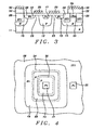
- Fig. 3 shows a cross section view of the pixel of this embodiment and Fig. 4 a top view.
- a P well 13 is formed in a substrate 11 of N type epitaxial silicon.
- An N well 15 is also formed in the substrate 11 of N type epitaxial silicon and surrounds the P well 13 as can be seen in Fig. 4.
- the P well 13 is P type silicon and the N well 15 is N type silicon.
- a first P + region 17 can be formed in the P well 13 and can be used to make electrical contact to the P well 13.
- a second P + region 25, which is not essential to the invention, can be formed in the N well 15. Active devices can be formed in the N well 15 using the second P + region 25.
- An N + region 19 is formed in part of the N well 15 and part of the substrate 11 and surrounds the P well 13 leaving a gap 23 between the inner periphery of the N + region 19 and the P well 13.
- the N well 15 can provide isolation for the pixel but a shallow trench isolation region 28 can also be formed in the N well 15 to provide isolation for the pixel.
- a layer of thin gate dielectric 26, usually a gate oxide, covers the surface of the pixel outside the regions of the shallow trench isolation regions so that the thin gate oxide 26 covers the N + region 19, the first P + region 17, the second P + region 25, the gap 23, and the P well 13. Appropriate contacts may be made through the gate dielectric 26 to regions below the gate dielectric 26 as desired.
- a gate electrode 20 is formed on the gate dielectric 26 over the gap 23 between the N + region 19 and the P well 13, and extends over part of the P well 13 and part of the N + region 19. In this example the gate electrode 20 is polysilicon.
- a metal mask 30, formed on a dielectric 32, can be used to shield the non active parts of the pixel from incident light.
- the gate electrode 20 is not shown in Fig. 4, the location of the gate electrode is shown by the dashed lines 34 and 36 with the gate electrode being located between the dashed lines 34 and 36.
- the N + region 19 is the key feature in this embodiment of the invention and is used to reduce the dark current and improve the sensitivity of the pixel.
- the P + region 19 extending all the way to the P well 13 would provide a surface saturated with holes and prevent the surface states from contributing to dark current generation.
- overlapping the N + region 19 with the P well 12 would produce a low breakdown junction and cause dark current generation at the junction. This is avoided by leaving a gap 23 between the N + region 19 and the P well 13, covering the gap 23 with the gate electrode 20.
- With the proper bias applied to the gate electrode 20 the region of the substrate 11 under the gate electrode 20 is depleted of electrons and the region of the P well 13 under the gate electrode 20 is accumulated with holes. This will reduce the dark current of the active pixel sensor.
- the gate electrode 20 is typically biased at the highest potential of the structure, often ground potential.
- the electrons that are generated in the depletion region around the P well 13 will be collected in that P well 13 to N substrate 11 diode, whereas the electrons that are generated outside the depletion region (e.g. deeper in the substrate) will be able to diffuse into adjacent pixels and even possibly recombine without being collected. Since the entire region around the P well 13 is covered by a thin gate dielectric 26, the depth of silicon that is depleted in this pixel is increased resulting in improved sensitivity as well as improved modulation transfer function.
Landscapes
- Solid State Image Pick-Up Elements (AREA)
- Transforming Light Signals Into Electric Signals (AREA)
Abstract
An active pixel sensor which provides reduced dark current, improved sensitivity, and improved modulation transfer function. An N well, surrounded by a P well is formed in a P type epitaxial substrate. A P+ region is formed extending from within the P well into the substrate leaving a gap between the P+ region and the N well. A gate dielectric is formed covering at least the gap, part of the P+ region, and part of the N well. A gate electrode is formed on the gate dielectric over the gap, part of the P+ region, and part of the N well. The gate electrode is biased so that the region of the substrate under the gate electrode is accumulated with holes and the region of the N well under the gate electrode is depleted of electrons. This will reduce the dark current and improve the sensitivity of the active pixel sensor. In a second embodiment the P type epitaxial substrate is replaced by an N type epitaxial substrate, the N well is replaced by a P well, N+ regions are replaced by P+ regions, and P+ regions are replaced by N+ regions. In this second embodiment the gate electrode is biased so that the region of the substrate under the gate electrode is depleted of electrons and the region of the P well under the gate electrode is accumulated with holes.
Description
- This invention relates to an active pixel sensor fabricated using standard CMOS processing and more particularly to dark current suppression and improved sensitivity in active pixel sensors fabricated using standard CMOS processing.
- U.S. Pat. No. 6,649,950 B2 to He et al. describes substantially covering the surface of a photodiode structure in order to reduce dark current due to surface damage to the photodiode structure.
- U.S. Pat. No. 6,621,064 B2 to Chen et al. describes a device utilizing a buried junction away from the surface to reduce dark current.
- U.S. Patent Application Publication No. US 2004/0046104 A1 by Rhodes describes a CMOS imager in which the floating diffusion is connected to a gate of a source follower transistor by a doped polysilicon contact to provide a better ohmic contact and reduce leakage into the substrate.
- The use of standard CMOS processing in the fabrication of active pixel sensors has enormous cost advantages. However, active pixel sensors fabricated using standard CMOS processing have a problem with dark current and sensitivity, particularly in applications which require high performance.
- It is a principle objective of this invention to provide an active pixel sensor fabricated using standard CMOS processing which has improved sensitivity and reduced dark current.
- This objective is achieved by fabricating an N well surrounded by a P well in a P type epitaxial substrate. The N well is located within the inner periphery of the P well. A P+ region is formed extending from within the P well near the inner periphery of the P well to a distance from the edge of the N well, leaving a gap between the P+ region and the N well. A gate dielectric, typically a gate oxide, is formed covering at least the gap between the P+ region and the edge of the N well. A gate electrode is formed on the gate dielectric over the gap between the P+ region and the edge of the N well and part of the N well. The gate electrode is typically formed from polysilicon.
- The gate electrode is biased so that the region of the substrate under the gate electrode is accumulated with holes and the region of the N well under the gate electrode is depleted of electrons. This will reduce the dark current and improve the sensitivity of the active pixel sensor. The gate electrodes are typically biased at the lowest potential of the structure which in this example is usually ground potential.
- In another embodiment this objective is achieved by fabricating a P well surrounded by an N well in an N type epitaxial substrate. The P well is located within the inner periphery of the N well. An N+ region is formed extending from within the N well near the inner periphery of the N well to a distance from the edge of the P well, leaving a gap between the N+ region and the P well. A gate dielectric, typically a gate oxide, is formed covering at least the gap between the N+ region and the edge of the P well. A gate electrode is formed on the gate dielectric over the gap between the N+ region and the edge of the P well and part of the P well. The gate electrode is typically formed from polysilicon.
- The gate electrode is biased so that the region of the substrate under the gate electrode is accumulated with electrons and the region of the P well under the gate electrode is depleted of holes. This will reduce the dark current and improve the sensitivity of the active pixel sensor. The gate electrodes are typically biased at the highest potential of the structure which in this example is usually ground potential.
-
- Fig. 1 shows a cross section view of the active pixel sensor of this invention formed in a P type epitaxial substrate.
- Fig. 2 shows a top view of the active pixel sensor of this invention formed in a P type epitaxial substrate.
- Fig. 3 shows a cross section view of the active pixel sensor of this invention formed in an N type epitaxial substrate.
- Fig. 4 shows a top view of the active pixel sensor of this invention formed in an N type epitaxial substrate.
- Refer now to Figs. 1 and 2 for a detailed description of a preferred embodiment of this invention. Fig. 1 shows a cross section view of the pixel of this embodiment and Fig. 2 a top view. In this embodiment an
N well 12 is formed in asubstrate 10 of P type epitaxial silicon. A P well 14 is also formed in thesubstrate 10 of P type epitaxial silicon and surrounds the N well 12 as can be seen in Fig. 2. TheN well 12 is N type silicon and theP well 14 is P type silicon. A first N+ region 16 can be formed in the N well 12 and can be used to make electrical contact to theN well 12. A second N+ region 24, which is not essential to the invention, can be formed in theP well 14. Active devices can be formed in the P well using the second N+ region 24. A P+region 18 is formed in part of theP well 14 and part of thesubstrate 10 and surrounds the N well 12 leaving agap 22 between the inner periphery of the P+ region 18 and the N well 12. - The
P well 14 can provide isolation for the pixel but a shallowtrench isolation region 28 can also be formed in theP well 14 to provide isolation for the pixel. A layer of thin gate dielectric 26, usually a gate oxide, covers the surface of the pixel outside the regions of the shallow trench isolation regions so that thethin gate oxide 26 covers the P+ region 18, the first N+ region 16, the second N+ region 24, thegap 22, and the N well 12. Appropriate contacts may be made through the gate dielectric 26 to regions below the gate dielectric 26 as desired. Agate electrode 20 is formed on the gate dielectric 26 over thegap 22 between the P+ region 18 and the N well 12, and extends over part of theN well 12 and part of the P+ region 18. In this example thegate electrode 20 is polysilicon. Ametal mask 30, formed on a dielectric 32, can be used to shield the non active parts of the pixel from incident light. - To improve the clarity of Fig. 2 the
gate electrode 20, the gate dielectric 26, themetal shield 30, and the dielectric 32 supporting themetal shield 30 are not shown in Fig. 2. Although thegate electrode 20 is not shown in Fig. 2, the location of the gate electrode is shown by thedashed lines dashed lines - The P+ region 18 is the key feature in this embodiment of the invention and is used to reduce the dark current and improve the sensitivity of the pixel. Ideally the P+ region 18 extending all the way to the
N well 12 would provide a surface saturated with holes and prevent the surface states from contributing to dark current generation. However, overlapping the P+ region 18 with theN well 12 would produce a low breakdown junction and cause dark current generation at the junction. This is avoided by leaving agap 22 between the P+ region 18 and the N well 12, covering thegap 22 with thegate electrode 20. With the proper bias applied to thegate electrode 20 the region of the substrate under thegate electrode 20 is accumulated with holes and the region of the N well 12 under thegate electrode 20 is depleted of electrons. This will reduce the dark current of the active pixel sensor. Thegate electrode 20 is typically biased at the lowest potential of the structure, often ground potential. - The electrons that are generated in the depletion region around the N well 12 will be collected in that N well 12 to
P substrate 10 diode, whereas the electrons that are generated outside the depletion region (e.g. deeper in the substrate) will be able to diffuse into adjacent pixels and even possibly recombine without being collected. Since the entire region around theN well 12 is covered by a thin gate dielectric 26, the depth of silicon that is depleted in this pixel is increased resulting in improved sensitivity as well as improved modulation transfer function. - Refer now to Figs. 3 and 4 for a detailed description of another preferred embodiment of this invention. Fig. 3 shows a cross section view of the pixel of this embodiment and Fig. 4 a top view. In this embodiment a
P well 13 is formed in asubstrate 11 of N type epitaxial silicon. An N well 15 is also formed in thesubstrate 11 of N type epitaxial silicon and surrounds the P well 13 as can be seen in Fig. 4. The P well 13 is P type silicon and the N well 15 is N type silicon. A first P+ region 17 can be formed in the P well 13 and can be used to make electrical contact to the P well 13. A second P+ region 25, which is not essential to the invention, can be formed in the N well 15. Active devices can be formed in the N well 15 using the second P+ region 25. An N+ region 19 is formed in part of the N well 15 and part of thesubstrate 11 and surrounds the P well 13 leaving agap 23 between the inner periphery of the N+ region 19 and the P well 13. - The N well 15 can provide isolation for the pixel but a shallow
trench isolation region 28 can also be formed in the N well 15 to provide isolation for the pixel. A layer ofthin gate dielectric 26, usually a gate oxide, covers the surface of the pixel outside the regions of the shallow trench isolation regions so that thethin gate oxide 26 covers the N+ region 19, the first P+ region 17, the second P+ region 25, thegap 23, and the P well 13. Appropriate contacts may be made through thegate dielectric 26 to regions below thegate dielectric 26 as desired. Agate electrode 20 is formed on thegate dielectric 26 over thegap 23 between the N+ region 19 and the P well 13, and extends over part of the P well 13 and part of the N+ region 19. In this example thegate electrode 20 is polysilicon. Ametal mask 30, formed on a dielectric 32, can be used to shield the non active parts of the pixel from incident light. - To improve the clarity of Fig. 4 the
gate electrode 20, thegate dielectric 26, themetal shield 30, and the dielectric 32 supporting themetal shield 30 are not shown in Fig. 4. Although thegate electrode 20 is not shown in Fig. 4, the location of the gate electrode is shown by the dashedlines lines - The N+ region 19 is the key feature in this embodiment of the invention and is used to reduce the dark current and improve the sensitivity of the pixel. Ideally the P+ region 19 extending all the way to the P well 13 would provide a surface saturated with holes and prevent the surface states from contributing to dark current generation. However, overlapping the N+ region 19 with the P well 12 would produce a low breakdown junction and cause dark current generation at the junction. This is avoided by leaving a
gap 23 between the N+ region 19 and the P well 13, covering thegap 23 with thegate electrode 20. With the proper bias applied to thegate electrode 20 the region of thesubstrate 11 under thegate electrode 20 is depleted of electrons and the region of the P well 13 under thegate electrode 20 is accumulated with holes. This will reduce the dark current of the active pixel sensor. Thegate electrode 20 is typically biased at the highest potential of the structure, often ground potential. - The electrons that are generated in the depletion region around the P well 13 will be collected in that P well 13 to
N substrate 11 diode, whereas the electrons that are generated outside the depletion region (e.g. deeper in the substrate) will be able to diffuse into adjacent pixels and even possibly recombine without being collected. Since the entire region around the P well 13 is covered by athin gate dielectric 26, the depth of silicon that is depleted in this pixel is increased resulting in improved sensitivity as well as improved modulation transfer function.
Claims (18)
- An active pixel sensor, comprising:a substrate formed of P type epitaxial silicon;an N well formed in said substrate wherein said N well is formed of N type silicon;a P well formed in said substrate wherein said P well has an inner periphery and an outer periphery, surrounds said N well, and is formed of P type silicon;an N+ region formed in said N well;a P+ region formed in part of said P well and part of said substrate wherein said P+ region extends from within said P well into said substrate toward said N well, thereby leaving a gap between said P+ region and said N well;a layer of gate dielectric formed over said gap, said N well, said N+ region, and at least part of said P+ region; anda gate electrode formed on said layer of gate dielectric over said gap, at least part of said N well, and at least part of said P+ region.
- The active pixel sensor of claim 1 wherein said gate dielectric is formed over all of said P+ region.
- The active pixel sensor of claim 1 wherein said dielectric is silicon dioxide.
- The active pixel sensor of claim 1 wherein said gate electrode is formed of polysilicon.
- The active pixel sensor of claim 1 further comprising a shallow trench isolation region in said P well.
- The active pixel sensor of claim 1 further comprising an opaque shield over said active pixel sensor except for said P+ region, said gap, said N region, and said N+ region.
- The active pixel sensor of claim 6 wherein said opaque shield is a metal shield.
- The active pixel sensor of claim 1 wherein said gate electrode is held at the lowest potential of the active pixel sensor.
- The active pixel sensor of claim 1 wherein electrical contact to said N well is made through said N+ region.
- An active pixel sensor, comprising:a substrate formed of N type epitaxial silicon;a P well formed in said substrate wherein said P well is formed of P type silicon;an N well formed in said substrate wherein said N well has an inner periphery and an outer periphery, surrounds said P well, and is formed of N type silicon;a P+ region formed in said P well;an N+ region formed in part of said N well and part of said substrate wherein said N+ region extends from within said N well into said substrate toward said P well, thereby leaving a gap between said N+ region and said P well;a layer of gate dielectric formed over said gap, said P well, said P+ region, and at least part of said N+ region; anda gate electrode formed on said layer of gate dielectric over said gap, at least part of said P well, and at least part of said N+ region.
- The active pixel sensor of claim 10 wherein said gate dielectric is formed over all of said N+ region.
- The active pixel sensor of claim 10 wherein said dielectric is silicon dioxide.
- The active pixel sensor of claim 10 wherein said gate electrode is formed of polysilicon.
- The active pixel sensor of claim 10 further comprising a shallow trench isolation region in said N well.
- The active pixel sensor of claim 10 further comprising an opaque shield over said active pixel sensor except for said N+ region, said gap, said P region, and said P+ region.
- The active pixel sensor of claim 15 wherein said opaque shield is a metal shield.
- The active pixel sensor of claim 10 wherein said gate electrode is held at the highest potential of the active pixel sensor.
- The active pixel sensor of claim 10 wherein electrical contact to said P well is made through said P+ region.
Applications Claiming Priority (1)
| Application Number | Priority Date | Filing Date | Title |
|---|---|---|---|
| US11/036,937 US7176532B2 (en) | 2004-07-22 | 2005-01-14 | CMOS active pixel sensor with improved dark current and sensitivity |
Publications (1)
| Publication Number | Publication Date |
|---|---|
| EP1681724A2 true EP1681724A2 (en) | 2006-07-19 |
Family
ID=36228529
Family Applications (1)
| Application Number | Title | Priority Date | Filing Date |
|---|---|---|---|
| EP06392001A Withdrawn EP1681724A2 (en) | 2005-01-14 | 2006-01-10 | CMOS active pixel sensor with improved dark current and sensitivity |
Country Status (2)
| Country | Link |
|---|---|
| US (1) | US7176532B2 (en) |
| EP (1) | EP1681724A2 (en) |
Cited By (2)
| Publication number | Priority date | Publication date | Assignee | Title |
|---|---|---|---|---|
| TWI465719B (en) * | 2010-08-09 | 2014-12-21 | Omnivision Tech Inc | Backside stimulated sensor with background current steering |
| US8987841B2 (en) | 2010-08-09 | 2015-03-24 | Omnivision Technologies, Inc. | Backside stimulated sensor with background current manipulation |
Families Citing this family (6)
| Publication number | Priority date | Publication date | Assignee | Title |
|---|---|---|---|---|
| US8497167B1 (en) * | 2007-01-17 | 2013-07-30 | National Semiconductor Corporation | EDS protection diode with pwell-nwell resurf |
| US8138531B2 (en) * | 2009-09-17 | 2012-03-20 | International Business Machines Corporation | Structures, design structures and methods of fabricating global shutter pixel sensor cells |
| EP2713409B1 (en) * | 2012-09-27 | 2020-08-26 | ams AG | Photodiode with a field electrode for reducing the space charge region |
| CN103811512B (en) * | 2014-03-17 | 2017-01-04 | 北京思比科微电子技术股份有限公司 | Image sensor pixel structure for preventing image dispersion and manufacturing method thereof |
| US9584744B2 (en) | 2015-06-23 | 2017-02-28 | Semiconductor Components Industries, Llc | Image sensors with voltage-biased trench isolation structures |
| EP3929986A1 (en) * | 2020-06-24 | 2021-12-29 | Ams Ag | Photodiode device with improved dark current |
Family Cites Families (13)
| Publication number | Priority date | Publication date | Assignee | Title |
|---|---|---|---|---|
| KR100190020B1 (en) * | 1996-02-21 | 1999-06-01 | 윤종용 | High voltage transistor and method of manufacturing thereof |
| KR100225411B1 (en) * | 1997-03-24 | 1999-10-15 | 김덕중 | Ldmos transistor device and method of manufacturing the same |
| US6639261B2 (en) | 1998-12-08 | 2003-10-28 | Micron Technology, Inc. | Method for forming a low leakage contact in a CMOS imager |
| US6680222B2 (en) * | 1999-11-05 | 2004-01-20 | Isetex, Inc | Split-gate virtual-phase CCD image sensor with a diffused lateral overflow anti-blooming drain structure and process of making |
| US6933488B2 (en) * | 2000-06-08 | 2005-08-23 | California Institute Of Technology | Variable electronic shutter in CMOS imager with improved anti smearing techniques |
| US6306700B1 (en) * | 2000-08-07 | 2001-10-23 | United Microelectronics Corp. | Method for forming high voltage devices compatible with low voltages devices on semiconductor substrate |
| US6621064B2 (en) | 2001-05-03 | 2003-09-16 | Texas Instruments Incorporated | CMOS photodiode having reduced dark current and improved light sensitivity and responsivity |
| US6512280B2 (en) * | 2001-05-16 | 2003-01-28 | Texas Instruments Incorporated | Integrated CMOS structure for gate-controlled buried photodiode |
| US6462365B1 (en) | 2001-11-06 | 2002-10-08 | Omnivision Technologies, Inc. | Active pixel having reduced dark current in a CMOS image sensor |
| US6545303B1 (en) * | 2001-11-06 | 2003-04-08 | Fillfactory | Method to increase conversion gain of an active pixel, and corresponding active pixel |
| US6750489B1 (en) * | 2002-10-25 | 2004-06-15 | Foveon, Inc. | Isolated high voltage PMOS transistor |
| US7019377B2 (en) * | 2002-12-17 | 2006-03-28 | Micrel, Inc. | Integrated circuit including high voltage devices and low voltage devices |
| US6972457B1 (en) * | 2004-04-09 | 2005-12-06 | Eastman Kodak Company | Imaging cell that has a long integration period and method of operating the imaging cell |
-
2005
- 2005-01-14 US US11/036,937 patent/US7176532B2/en not_active Expired - Lifetime
-
2006
- 2006-01-10 EP EP06392001A patent/EP1681724A2/en not_active Withdrawn
Cited By (2)
| Publication number | Priority date | Publication date | Assignee | Title |
|---|---|---|---|---|
| TWI465719B (en) * | 2010-08-09 | 2014-12-21 | Omnivision Tech Inc | Backside stimulated sensor with background current steering |
| US8987841B2 (en) | 2010-08-09 | 2015-03-24 | Omnivision Technologies, Inc. | Backside stimulated sensor with background current manipulation |
Also Published As
| Publication number | Publication date |
|---|---|
| US20060017072A1 (en) | 2006-01-26 |
| US7176532B2 (en) | 2007-02-13 |
Similar Documents
| Publication | Publication Date | Title |
|---|---|---|
| CN109804472B (en) | Avalanche photodiode | |
| US6329679B1 (en) | Photodiode with increased photocollection area for image sensor | |
| US9899448B2 (en) | Semiconductor device having SOI substrate | |
| US7329557B2 (en) | Method of manufacturing solid-state imaging device with P-type diffusion layers | |
| US10861997B2 (en) | Single photon avalanche gate sensor device | |
| JP5971565B2 (en) | Solid-state imaging device | |
| US20100301442A1 (en) | Optical semiconductor device | |
| JP3727639B2 (en) | Solid-state imaging device | |
| US7176532B2 (en) | CMOS active pixel sensor with improved dark current and sensitivity | |
| US6566678B1 (en) | Semiconductor device having a solid-state image sensor | |
| JP4854216B2 (en) | Imaging apparatus and imaging system | |
| US9754991B2 (en) | Semiconductor device and method of manufacturing thereof | |
| US6690074B1 (en) | Radiation resistant semiconductor device structure | |
| US20160013224A1 (en) | Photoelectric conversion device | |
| JP4354931B2 (en) | Solid-state imaging device and manufacturing method thereof | |
| JP2006332287A (en) | Thin film diode | |
| US12324260B2 (en) | Multiplying image sensor | |
| US7645652B2 (en) | CMOS image sensor and method for fabricating the same | |
| US20090166691A1 (en) | Image Sensor and Method of Manufacturing the Same | |
| US7061031B1 (en) | High-sensitivity image sensor and fabrication method thereof | |
| JP2007323390A (en) | Solid-state imaging device | |
| KR101348823B1 (en) | Solid-state imaging device and manufacturing method thereof | |
| KR20230021300A (en) | Spad pixel structure of backside illuminated image sensor | |
| KR20230112621A (en) | photoelectric converter | |
| JP2006179825A (en) | Amplification type solid-state image sensor |
Legal Events
| Date | Code | Title | Description |
|---|---|---|---|
| PUAI | Public reference made under article 153(3) epc to a published international application that has entered the european phase |
Free format text: ORIGINAL CODE: 0009012 |
|
| AK | Designated contracting states |
Kind code of ref document: A2 Designated state(s): AT BE BG CH CY CZ DE DK EE ES FI FR GB GR HU IE IS IT LI LT LU LV MC NL PL PT RO SE SI SK TR |
|
| AX | Request for extension of the european patent |
Extension state: AL BA HR MK YU |
|
| STAA | Information on the status of an ep patent application or granted ep patent |
Free format text: STATUS: THE APPLICATION HAS BEEN WITHDRAWN |
|
| 18D | Application deemed to be withdrawn |
Effective date: 20080101 |
|
| 18W | Application withdrawn |
Effective date: 20081121 |