EP1679586A1 - Implementation of digital signal processing functions using maximal efficiency and minimal energy dissipation - Google Patents
Implementation of digital signal processing functions using maximal efficiency and minimal energy dissipation Download PDFInfo
- Publication number
- EP1679586A1 EP1679586A1 EP05020717A EP05020717A EP1679586A1 EP 1679586 A1 EP1679586 A1 EP 1679586A1 EP 05020717 A EP05020717 A EP 05020717A EP 05020717 A EP05020717 A EP 05020717A EP 1679586 A1 EP1679586 A1 EP 1679586A1
- Authority
- EP
- European Patent Office
- Prior art keywords
- logic module
- carry
- save
- logic
- accumulator
- Prior art date
- Legal status (The legal status is an assumption and is not a legal conclusion. Google has not performed a legal analysis and makes no representation as to the accuracy of the status listed.)
- Ceased
Links
Images

Classifications
-
- G—PHYSICS
- G06—COMPUTING OR CALCULATING; COUNTING
- G06F—ELECTRIC DIGITAL DATA PROCESSING
- G06F7/00—Methods or arrangements for processing data by operating upon the order or content of the data handled
- G06F7/38—Methods or arrangements for performing computations using exclusively denominational number representation, e.g. using binary, ternary, decimal representation
- G06F7/48—Methods or arrangements for performing computations using exclusively denominational number representation, e.g. using binary, ternary, decimal representation using non-contact-making devices, e.g. tube, solid state device; using unspecified devices
- G06F7/50—Adding; Subtracting
- G06F7/505—Adding; Subtracting in bit-parallel fashion, i.e. having a different digit-handling circuit for each denomination
- G06F7/509—Adding; Subtracting in bit-parallel fashion, i.e. having a different digit-handling circuit for each denomination for multiple operands, e.g. digital integrators
-
- G—PHYSICS
- G06—COMPUTING OR CALCULATING; COUNTING
- G06F—ELECTRIC DIGITAL DATA PROCESSING
- G06F7/00—Methods or arrangements for processing data by operating upon the order or content of the data handled
- G06F7/38—Methods or arrangements for performing computations using exclusively denominational number representation, e.g. using binary, ternary, decimal representation
- G06F7/48—Methods or arrangements for performing computations using exclusively denominational number representation, e.g. using binary, ternary, decimal representation using non-contact-making devices, e.g. tube, solid state device; using unspecified devices
- G06F7/50—Adding; Subtracting
- G06F7/505—Adding; Subtracting in bit-parallel fashion, i.e. having a different digit-handling circuit for each denomination
- G06F7/509—Adding; Subtracting in bit-parallel fashion, i.e. having a different digit-handling circuit for each denomination for multiple operands, e.g. digital integrators
- G06F7/5095—Adding; Subtracting in bit-parallel fashion, i.e. having a different digit-handling circuit for each denomination for multiple operands, e.g. digital integrators word-serial, i.e. with an accumulator-register
Definitions
- Digital signal processing functions may be implemented in silicon using a number of different processes or methodologies.
- the implementation of digital signal processing circuits such as digital filters, multipliers, and accumulators may be performed using one or more design building blocks or logic modules. These design building blocks or logic modules may comprise multi-operand adders and registers.
- the logic modules may not be optimally designed.
- the overall chip area used to implement the logic module may be too large.
- the overall processing delay associated with the components of the logic module may be suboptimal.
- the power consumed by the logic module may be excessive for the digital signal processing functions implemented.
- Various aspects of the invention provide a system and a method of implementing integrated circuit logic modules that provide maximum efficiency and minimal energy dissipated per unit of operation.
- a four input / two output carry-save accumulator may be used as a logic module that exhibits this maximum efficiency and minimal energy dissipation.
- a method of implementing signal processing functions on an integrated circuit chip comprises using a minimum cell area for each of one or more cells of one or more logic modules of the integrated circuit chip such that an efficiency of each of the one or more logic modules is maximized.
- the method further comprises using four carry-save adders in each of the one or more logic modules.
- a method of designing a logic module using one or more cells, wherein the logic module implements one or more digital signal processing functions comprises determining a minimum circuit area of the logic module. The minimum circuit area generates a maximum efficiency of the logic module.
- a logic module for implementing highly efficient digital signal processing functions on an integrated circuit chip comprises four carry-save adders and two registers.
- the four carry-save adders may be arranged in a tree configuration such that its total processing delay is equivalent to that of the sum of the processing delays of the three carry-save adders and one register.
- a method of implementing signal processing functions on an integrated circuit chip comprising:
- said four carry-save adders are configured as a tree structure.
- each of said one or more logic modules dissipates a minimum energy per addition operation.
- each of said one or more logic modules comprises a six input / two output multi-operand carry-save adder and two registers, said six input / two output multi-operand carry-save adder implemented using said four carry-save adders configured in a tree structure.
- said one or more logic modules is used to implement one or more multipliers.
- said one or more logic modules is used to implement one or more digital filters.
- said one or more digital filters comprises a FIR filter.
- said one or more digital filters comprises an IIR filter.
- a method of designing a logic module using one or more cells comprising determining a minimum cell height associated with a first circuit area of said logic module, said first circuit area associated with generating a maximum efficiency of said logic module.
- said logic module comprises an accumulator, said accumulator comprising a six input / two output multi-operand carry-save adder and two registers.
- said six input / two output multi-operand carry-save adder comprises four carry-save adders.
- said four carry-save adders are arranged in a tree structure.
- said efficiency is computed by dividing a number of additions performed by said logic module by a product of said first circuit area and a clock period, said clock period associated with a clock that is used to process data using said logic module.
- said clock period is equal to a processing delay of said logic module.
- said processing delay corresponds to a critical path delay of said logic module.
- said first circuit area is equal to the sum of a second circuit area corresponding to one or more registers in said logic module, and a third circuit area corresponding to one or more carry-save adders in said logic module.
- a logic module for implementing highly efficient digital signal processing functions on an integrated circuit chip comprising four carry-save adders.
- the logic module further comprises two registers.
- said four carry-save adders are arranged in a tree structure such that minimum energy is dissipated per full adder.
- said logic module comprises a four input / two output carry-save accumulator.
- said logic module comprises a six input / two output carry-save adder.
- said four carry-save adders and said two registers generates a processing delay equivalent to that of the sum of the processing delays of three of said four carry-save adders and one register.
- Figure 1 is a functional block diagram of a four input / two output carry-save accumulator employed in the implementation of one or more digital signal processing circuits of an integrated circuit chip, in accordance with an embodiment of the invention.
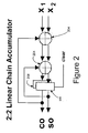
- Figure 2 is a functional block diagram of a two input / two output linear chain carry-save accumulator.
- the logic module may be defined as an elementary digital signal processing (DSP) unit that is used in the design and implementation of various digital signal processing circuitries.
- DSP elementary digital signal processing
- Various aspects of the invention provide a method of utilizing one or more logic modules to implement a variety of digital signal processing circuitries.
- These logic modules may comprise one or more accumulators or multi-operand adders, for example.
- each of the one or more accumulators may comprise one or more multi-operand adders.
- multipliers and digital filters may be implemented, for example.
- the digital filters may comprise a finite impulse response (FIR) filter or an infinite impulse response (IIR) filter, for example.
- the logic module comprises an implementation of a carry-save accumulator.
- the carry-save accumulator comprises four inputs and two outputs.
- the four input / two output carry-save accumulator may be implemented by using a 6:2 compressor along with two registers.
- the 6:2 compressor may be implemented using four 3:2 compressors.
- the 6:2 compressor with two output registers can be used as a generic building block to implement optimally pipelined DSP functions such as multipliers or digital filters.
- the 6:2 compressor may be implemented using 3:2 compressors that are arranged in a tree configuration or tree structure. Aspects of the invention allow the use of one or more 6:2 compressors for implementing various digital signalprocessing circuitries on an integrated circuit chip.
- a design parameter referred to as the efficiency may be computed for the logic module.
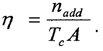
- the efficiency, ⁇ is computed by dividing the number of additions, n add , performed by the logic module by the product of T c and A.
- T c is defined as the cycle time required for the logic module to perform the number of additions, n add .
- A is defined as the circuit area required to implement the logic module. As may be easily observed, the efficiency increases as the number of additions performed increases. Also, the efficiency increases as the area of the logic module decreases.
- the variable T c is related to the overall processing delay associated with the logic module.
- the overall processing delay of the logic module determines the minimum clock period or maximum clocking frequency used to drive the logic module. For example, one or more registers within a logic module may require clocking at a suitable clock frequency in order to adequately process data at its inputs. Its clock period may be larger than or equal to the overall processing delay associated with the logic module.
- the circuit area of the logic module comprises the areas of one or more cells. The height of each cell of the one or more cells is linearly related to the area of each cell. Alternatively, the width of each cell of the one or more cells is linearly related to the area of each cell.
- a logic module is designed such that its efficiency, ⁇ , is as high as possible.
- the efficiency may be alternatively described as an AT complexity.
- the AT complexity is equivalent to the product of the area and the overall processing delay of the logic module.
- a circuit designer will want the AT complexity to be as low as possible. Since increases in circuit area of an integrated circuit are associated with increases in manufacturing costs, smaller circuit areas are used to implement a logic module. Correspondingly, smaller cells (associated with smaller cell areas) are used to implement a logic module. Using smaller cell heights for each cell, for example, may reduce the cell area.
- an optimal value for the efficiency of a carry-save accumulator occurs when a total of four 3:2 compressors (carry-save adders) are utilized in the 6:2 compressor and the four 3:2 compressors are configured as a tree configuration or tree structure.
- the 6:2 compressor that is used in such a tree structure is subject to a processing delay equivalent to that of three 3:2 compressors, or three full adders.
- the processing delay of the 6:2 compressor is independent of the word length of its input vectors since the 3:2 compressors comprise four carry-save adders.
- the four carry-save adders do not propagate carries, and as a consequence, the 6:2 compressor does not propagate any carries.
- Figure 1 is a functional block diagram of a four input / two output carry-save accumulator employed in the implementation of one or more digital signal processing functions of an integrated circuit chip, in accordance with an embodiment of the invention.
- the four input / two output accumulator incorporates the use of a six input / two output multi-operand carry-save adder.
- the multi-operand carry-save adder eliminates carry propagation by handing redundant carry-save results to the next adder in the processing chain.
- the carry-save accumulator illustrated in Figure 1 may be described as a 4:2 accumulator using a 3:2 compression tree structure, since it utilizes four 3:2 compressors (or four carry-save adders) 104 arranged in a tree configuration.
- the 4:2 accumulator using a 3:2 compression tree structure may be referred to as a 4:2 tree accumulator.
- the 4:2 tree accumulator has four inputs and two outputs.
- Each of the four inputs x 1 , x 2 , x 3 , and x 4 may comprise a vector of any word length.
- the vector may comprise a 32 bit word.
- the outputs Co (carry) and So (sum) are fed back as inputs into two of the four 3:2 compressors 104 of the 4:2 tree accumulator.
- the 4:2 tree accumulator comprises two registers 108 as shown.
- the two registers 108 provide carry and sum outputs to the next logic module in a pipeline, for example.
- the processing delay (T) of the 4:2 tree accumulator is equal to the sum of the register delay ( ⁇ reg ) and the delay through the critical path of the four carry-save adder tree (3 ⁇ add ) .
- the energy consumed per addition is significantly lower than any other carry-save accumulator having a comparable efficiency, when using any number of full adders configured either in a linear chain or in a tree structure.
- the 2:2 linear chain carry-save accumulator comprises two 3:2 compressors (or full adders) 204 arranged linearly.
- the two inputs of the 2:2 linear chain carry-save accumulator comprise the vectors X 1 and X 2 .
- the 2:2 linear chain carry-save accumulator also comprises two registers 208.
- the two registers 208 provide outputs C 0 and S 0 that are fed back as inputs into each of the two 3:2 compressors 204.
- the 2:2 linear chain carry-save accumulator provides a value for the efficiency that is similar to that of the 4:2 tree accumulator
- the 2:2 linear chain carry-save accumulator consumes significantly more energy per addition.
- the 2:2 linear chain carry-save accumulator dissipates more energy per addition operation compared to the 4:2 tree accumulator.
- an addition operation provided by the 2:2 linear chain carry-save accumulator of Figure 2 uses significantly more energy than that of an addition operation provided by the 4:2 tree accumulator of Figure 1.
- a maximum value for the efficiency, ⁇ occurs when the area of the individual logic cells in the multi-operand adders is close to a minimum value given by the resolution of the lithographic process that is used to manufacture the integrated circuit.
Landscapes
- Physics & Mathematics (AREA)
- General Physics & Mathematics (AREA)
- Engineering & Computer Science (AREA)
- Computational Mathematics (AREA)
- Mathematical Analysis (AREA)
- Pure & Applied Mathematics (AREA)
- Theoretical Computer Science (AREA)
- Computing Systems (AREA)
- Mathematical Optimization (AREA)
- General Engineering & Computer Science (AREA)
- Design And Manufacture Of Integrated Circuits (AREA)
- Power Sources (AREA)
Abstract
Description
- [Not Applicable]
- [Not Applicable]
- [Not Applicable]
- Digital signal processing functions may be implemented in silicon using a number of different processes or methodologies. The implementation of digital signal processing circuits such as digital filters, multipliers, and accumulators may be performed using one or more design building blocks or logic modules. These design building blocks or logic modules may comprise multi-operand adders and registers.
- In many instances, the logic modules may not be optimally designed. For example, the overall chip area used to implement the logic module may be too large. In other instances, the overall processing delay associated with the components of the logic module may be suboptimal. Yet, in other instances, the power consumed by the logic module may be excessive for the digital signal processing functions implemented.
- The limitations and disadvantages of conventional and traditional approaches will become apparent to one of skill in the art, through comparison of such systems with some aspects of the present invention as set forth in the remainder of the present application with reference to the drawings.
- Various aspects of the invention provide a system and a method of implementing integrated circuit logic modules that provide maximum efficiency and minimal energy dissipated per unit of operation. In a representative embodiment, a four input / two output carry-save accumulator may be used as a logic module that exhibits this maximum efficiency and minimal energy dissipation.
- In a representative embodiment, a method of implementing signal processing functions on an integrated circuit chip comprises using a minimum cell area for each of one or more cells of one or more logic modules of the integrated circuit chip such that an efficiency of each of the one or more logic modules is maximized. The method further comprises using four carry-save adders in each of the one or more logic modules.
- In another representative embodiment, a method of designing a logic module using one or more cells, wherein the logic module implements one or more digital signal processing functions comprises determining a minimum circuit area of the logic module. The minimum circuit area generates a maximum efficiency of the logic module.
- In a representative embodiment, a logic module for implementing highly efficient digital signal processing functions on an integrated circuit chip comprises four carry-save adders and two registers. The four carry-save adders may be arranged in a tree configuration such that its total processing delay is equivalent to that of the sum of the processing delays of the three carry-save adders and one register.
- According to an aspect of the invention, a method of implementing signal processing functions on an integrated circuit chip is provided comprising:
- using a minimum cell area for each of one or more cells of one or more logic modules of said integrated circuit chip such that an efficiency of each of said one or more logic modules is maximized; and
- using four carry-save adders in each of said one or more logic modules.
- Advantageously, said four carry-save adders are configured as a tree structure.
- Advantageously, said efficiency is computed using the equation,
- Advantageously, each of said one or more logic modules dissipates a minimum energy per addition operation.
- Advantageously, each of said one or more logic modules comprises a six input / two output multi-operand carry-save adder and two registers, said six input / two output multi-operand carry-save adder implemented using said four carry-save adders configured in a tree structure.
- Advantageously, said one or more logic modules is used to implement one or more multipliers.
- Advantageously, said one or more logic modules is used to implement one or more digital filters.
- Advantageously, said one or more digital filters comprises a FIR filter.
- Advantageously, said one or more digital filters comprises an IIR filter.
- According to an aspect of the invention, a method of designing a logic module using one or more cells is provided, said logic module implementing one or more digital signal processing functions, said method comprising determining a minimum cell height associated with a first circuit area of said logic module, said first circuit area associated with generating a maximum efficiency of said logic module.
- Advantageously, said logic module comprises an accumulator, said accumulator comprising a six input / two output multi-operand carry-save adder and two registers.
- Advantageously, said six input / two output multi-operand carry-save adder comprises four carry-save adders.
- Advantageously, said four carry-save adders are arranged in a tree structure.
- Advantageously, said efficiency is computed by dividing a number of additions performed by said logic module by a product of said first circuit area and a clock period, said clock period associated with a clock that is used to process data using said logic module.
- Advantageously, said clock period is equal to a processing delay of said logic module.
- Advantageously, said processing delay corresponds to a critical path delay of said logic module.
- Advantageously, said first circuit area is equal to the sum of a second circuit area corresponding to one or more registers in said logic module, and a third circuit area corresponding to one or more carry-save adders in said logic module.
- According to an aspect of the invention, a logic module for implementing highly efficient digital signal processing functions on an integrated circuit chip is provided comprising four carry-save adders.
- Advantageously, the logic module further comprises two registers.
- Advantageously, said four carry-save adders are arranged in a tree structure such that minimum energy is dissipated per full adder.
- Advantageously, said logic module comprises a four input / two output carry-save accumulator.
- Advantageously, said logic module comprises a six input / two output carry-save adder.
- Advantageously, said four carry-save adders and said two registers generates a processing delay equivalent to that of the sum of the processing delays of three of said four carry-save adders and one register.
- These and other advantages, aspects, and novel features of the present invention, as well as details of illustrated embodiments, thereof, will be more fully understood from the following description and drawings.
- Figure 1 is a functional block diagram of a four input / two output carry-save accumulator employed in the implementation of one or more digital signal processing circuits of an integrated circuit chip, in accordance with an embodiment of the invention.
- Figure 2 is a functional block diagram of a two input / two output linear chain carry-save accumulator.
- Various aspects of the present invention provide at least a system and method that maximizes the efficiency of a logic module used in the implementation of one or more digital signal processing functions when fabricating an integrated circuit chip. The logic module may be defined as an elementary digital signal processing (DSP) unit that is used in the design and implementation of various digital signal processing circuitries.
- Various aspects of the invention provide a method of utilizing one or more logic modules to implement a variety of digital signal processing circuitries. These logic modules may comprise one or more accumulators or multi-operand adders, for example. In a representative embodiment, each of the one or more accumulators may comprise one or more multi-operand adders. By concatenating the one or more accumulators together, one or more multipliers and digital filters may be implemented, for example. The digital filters may comprise a finite impulse response (FIR) filter or an infinite impulse response (IIR) filter, for example.
- In a representative embodiment, the logic module comprises an implementation of a carry-save accumulator. The carry-save accumulator comprises four inputs and two outputs. The four input / two output carry-save accumulator may be implemented by using a 6:2 compressor along with two registers. The 6:2 compressor may be implemented using four 3:2 compressors. The 6:2 compressor with two output registers can be used as a generic building block to implement optimally pipelined DSP functions such as multipliers or digital filters. In a representative embodiment, the 6:2 compressor may be implemented using 3:2 compressors that are arranged in a tree configuration or tree structure. Aspects of the invention allow the use of one or more 6:2 compressors for implementing various digital signalprocessing circuitries on an integrated circuit chip.
- A design parameter referred to as the efficiency may be computed for the logic module. The efficiency may be defined by the following equation:

The efficiency, η, is computed by dividing the number of additions, n add , performed by the logic module by the product of T c and A. T c is defined as the cycle time required for the logic module to perform the number of additions, n add . A is defined as the circuit area required to implement the logic module. As may be easily observed, the efficiency increases as the number of additions performed increases. Also, the efficiency increases as the area of the logic module decreases. - The variable T c is related to the overall processing delay associated with the logic module. The overall processing delay of the logic module determines the minimum clock period or maximum clocking frequency used to drive the logic module. For example, one or more registers within a logic module may require clocking at a suitable clock frequency in order to adequately process data at its inputs. Its clock period may be larger than or equal to the overall processing delay associated with the logic module. The circuit area of the logic module comprises the areas of one or more cells. The height of each cell of the one or more cells is linearly related to the area of each cell. Alternatively, the width of each cell of the one or more cells is linearly related to the area of each cell.
- Ideally, a logic module is designed such that its efficiency, η, is as high as possible. The efficiency may be alternatively described as an AT complexity. The AT complexity is equivalent to the product of the area and the overall processing delay of the logic module. A circuit designer will want the AT complexity to be as low as possible. Since increases in circuit area of an integrated circuit are associated with increases in manufacturing costs, smaller circuit areas are used to implement a logic module. Correspondingly, smaller cells (associated with smaller cell areas) are used to implement a logic module. Using smaller cell heights for each cell, for example, may reduce the cell area.
- With respect to various aspects of the present invention, an optimal value for the efficiency of a carry-save accumulator occurs when a total of four 3:2 compressors (carry-save adders) are utilized in the 6:2 compressor and the four 3:2 compressors are configured as a tree configuration or tree structure. The 6:2 compressor that is used in such a tree structure is subject to a processing delay equivalent to that of three 3:2 compressors, or three full adders. The processing delay of the 6:2 compressor is independent of the word length of its input vectors since the 3:2 compressors comprise four carry-save adders. The four carry-save adders do not propagate carries, and as a consequence, the 6:2 compressor does not propagate any carries.
- Figure 1 is a functional block diagram of a four input / two output carry-save accumulator employed in the implementation of one or more digital signal processing functions of an integrated circuit chip, in accordance with an embodiment of the invention. The four input / two output accumulator incorporates the use of a six input / two output multi-operand carry-save adder. The multi-operand carry-save adder eliminates carry propagation by handing redundant carry-save results to the next adder in the processing chain. The carry-save accumulator illustrated in Figure 1 may be described as a 4:2 accumulator using a 3:2 compression tree structure, since it utilizes four 3:2 compressors (or four carry-save adders) 104 arranged in a tree configuration. Hereinafter, the 4:2 accumulator using a 3:2 compression tree structure may be referred to as a 4:2 tree accumulator. The 4:2 tree accumulator has four inputs and two outputs. Each of the four inputs x1, x2, x3, and x4 may comprise a vector of any word length. For example, the vector may comprise a 32 bit word. The outputs Co (carry) and So (sum) are fed back as inputs into two of the four 3:2
compressors 104 of the 4:2 tree accumulator. Furthermore, the 4:2 tree accumulator comprises tworegisters 108 as shown. The tworegisters 108 provide carry and sum outputs to the next logic module in a pipeline, for example. As may be seen from Figure 1, the processing delay and the circuit area associated with the 4:2 tree accumulator may be defined by the following equations:

The processing delay (T) of the 4:2 tree accumulator is equal to the sum of the register delay (τ reg ) and the delay through the critical path of the four carry-save adder tree (3·τ add ). One may obtain an optimal value for the efficiency when using the 4:2 tree accumulator shown in Figure 1. Furthermore, the energy consumed per addition is significantly lower than any other carry-save accumulator having a comparable efficiency, when using any number of full adders configured either in a linear chain or in a tree structure. Compared to that of a 2:2 (two input / two output) linear chain carry-save accumulator, as illustrated in Figure 2, there is approximately a 29% reduction in the amount of energy dissipated per addition when using the 4:2 tree accumulator, given the same input vector word lengths. The 2:2 linear chain carry-save accumulator comprises two 3:2 compressors (or full adders) 204 arranged linearly. The two inputs of the 2:2 linear chain carry-save accumulator comprise the vectors X1 and X2. The 2:2 linear chain carry-save accumulator also comprises tworegisters 208. The tworegisters 208 provide outputs C0 and S0 that are fed back as inputs into each of the two 3:2compressors 204. Although the 2:2 linear chain carry-save accumulator provides a value for the efficiency that is similar to that of the 4:2 tree accumulator, the 2:2 linear chain carry-save accumulator consumes significantly more energy per addition. In other words, the 2:2 linear chain carry-save accumulator dissipates more energy per addition operation compared to the 4:2 tree accumulator. As a consequence, an addition operation provided by the 2:2 linear chain carry-save accumulator of Figure 2 uses significantly more energy than that of an addition operation provided by the 4:2 tree accumulator of Figure 1. A maximum value for the efficiency, η, occurs when the area of the individual logic cells in the multi-operand adders is close to a minimum value given by the resolution of the lithographic process that is used to manufacture the integrated circuit. - While the invention has been described with reference to certain embodiments, it will be understood by those skilled in the art that various changes may be made and equivalents may be substituted without departing from the scope of the invention. In addition, many modifications may be made to adapt a particular situation or material to the teachings of the invention without departing from its scope. Therefore, it is intended that the invention not be limited to the particular embodiments disclosed, but that the invention will include all embodiments falling within the scope of the appended claims.
Claims (10)
- A method of implementing signal processing functions on an integrated circuit chip comprising:using a minimum cell area for each of one or more cells of one or more logic modules of said integrated circuit chip such that an efficiency of each of said one or more logic modules is maximized; andusing four carry-save adders in each of said one or more logic modules.
- The method of Claim 1 wherein said four carry-save adders are configured as a tree structure.
- The method of Claim 2 wherein said efficiency is computed using the equation,

- The method of Claim 1 wherein each of said one or more logic modules dissipates a minimum energy per addition operation.
- A method of designing a logic module using one or more cells, said logic module implementing one or more digital signal processing functions, said method comprising determining a minimum cell height associated with a first circuit area of said logic module, said first circuit area associated with generating a maximum efficiency of said logic module.
- The method of Claim 5 wherein said logic module comprises an accumulator, said accumulator comprising a six input / two output multi-operand carry-save adder and two registers.
- A logic module for implementing highly efficient digital signal processing functions on an integrated circuit chip comprising four carry-save adders.
- The logic module of Claim 7 further comprising two registers.
- The logic module of Claim 8 wherein said four carry-save adders are arranged in a tree structure such that minimum energy is dissipated per full adder.
- The logic module of Claim 9 wherein said logic module comprises a four input / two output carry-save accumulator.
Applications Claiming Priority (1)
| Application Number | Priority Date | Filing Date | Title |
|---|---|---|---|
| US11/029,990 US8601048B2 (en) | 2005-01-05 | 2005-01-05 | Implementation of digital signal processing functions using maximal efficiency and minimal energy dissipation |
Publications (1)
| Publication Number | Publication Date |
|---|---|
| EP1679586A1 true EP1679586A1 (en) | 2006-07-12 |
Family
ID=35160094
Family Applications (1)
| Application Number | Title | Priority Date | Filing Date |
|---|---|---|---|
| EP05020717A Ceased EP1679586A1 (en) | 2005-01-05 | 2005-09-22 | Implementation of digital signal processing functions using maximal efficiency and minimal energy dissipation |
Country Status (4)
| Country | Link |
|---|---|
| US (1) | US8601048B2 (en) |
| EP (1) | EP1679586A1 (en) |
| CN (1) | CN100449553C (en) |
| TW (1) | TW200705972A (en) |
Families Citing this family (2)
| Publication number | Priority date | Publication date | Assignee | Title |
|---|---|---|---|---|
| CN103955585B (en) * | 2014-05-13 | 2017-02-15 | 复旦大学 | FIR (finite impulse response) filter structure for low-power fault-tolerant circuit |
| CN113805840B (en) * | 2021-11-18 | 2022-05-03 | 南京风兴科技有限公司 | Fast accumulator |
Citations (3)
| Publication number | Priority date | Publication date | Assignee | Title |
|---|---|---|---|---|
| US4769780A (en) * | 1986-02-10 | 1988-09-06 | International Business Machines Corporation | High speed multiplier |
| US5623683A (en) * | 1992-12-30 | 1997-04-22 | Intel Corporation | Two stage binary multiplier |
| US20030098870A1 (en) * | 2001-11-27 | 2003-05-29 | Michio Komoda | Linear Filter circuit |
Family Cites Families (5)
| Publication number | Priority date | Publication date | Assignee | Title |
|---|---|---|---|---|
| US4228520A (en) * | 1979-05-04 | 1980-10-14 | International Business Machines Corporation | High speed multiplier using carry-save/propagate pipeline with sparse carries |
| US5349676A (en) * | 1991-02-11 | 1994-09-20 | General Electric Company | Data acquisition systems with programmable bit-serial digital signal processors |
| US5220525A (en) * | 1991-11-04 | 1993-06-15 | Motorola, Inc. | Recoded iterative multiplier |
| US6065033A (en) * | 1997-02-28 | 2000-05-16 | Digital Equipment Corporation | Wallace-tree multipliers using half and full adders |
| US6615229B1 (en) * | 2000-06-29 | 2003-09-02 | Intel Corporation | Dual threshold voltage complementary pass-transistor logic implementation of a low-power, partitioned multiplier |
-
2005
- 2005-01-05 US US11/029,990 patent/US8601048B2/en not_active Expired - Fee Related
- 2005-09-22 EP EP05020717A patent/EP1679586A1/en not_active Ceased
-
2006
- 2006-01-04 TW TW095100349A patent/TW200705972A/en unknown
- 2006-01-05 CN CNB2006100025381A patent/CN100449553C/en not_active Expired - Fee Related
Patent Citations (3)
| Publication number | Priority date | Publication date | Assignee | Title |
|---|---|---|---|---|
| US4769780A (en) * | 1986-02-10 | 1988-09-06 | International Business Machines Corporation | High speed multiplier |
| US5623683A (en) * | 1992-12-30 | 1997-04-22 | Intel Corporation | Two stage binary multiplier |
| US20030098870A1 (en) * | 2001-11-27 | 2003-05-29 | Michio Komoda | Linear Filter circuit |
Non-Patent Citations (4)
| Title |
|---|
| CADENCE DATA SHEET: "SMIC-CADENCE LOW POWER DIGITAL REFERENCE FLOW FOR ENERGY-EFFICIENT 130 NANOMETER SOC DESIGNS", 2004, pages 1-4, XP002352528, Retrieved from the Internet <URL:http://www.cadence.com/datasheets/smic_joint_ds.pdf> [retrieved on 20051103] * |
| INTERNET FORUM: DEEPCHIP: "8 Engineers Discussing 7 Types Of Adder Harware Implementations", 16 February 2000 (2000-02-16), pages 1 - 4, XP002352529, Retrieved from the Internet <URL:http://www.deepchip.com/items/0343-13.html> [retrieved on 20051103] * |
| PAOLO IENNE, AJAY K. VERMA, FEDERAL INSTITUTE OF TECHNOLOGY LAUSANNE, PROCESSOR ARCHITECTURE LABORATORY: "Arithmetic Transformations to Maximise the Use of Compressor Trees", January 2004 (2004-01-01), pages 1 - 6, XP002352526, Retrieved from the Internet <URL:http://lapwww.epfl.ch/publications> [retrieved on 20051103] * |
| THOMAS K. CALLAWAY, EARL E. SWARTZLANDER, JR., DEPARTMENT OF ELECTRICAL AND COMPUTER ENGINEERING, UNIVERSITY OF TEXAS AT AUSTIN: "Optimizing Arithmetic Elements For Signal Processing", 28 October 1992 (1992-10-28), pages 91 - 100, XP002352527, Retrieved from the Internet <URL:http://ieeexplore.ieee.org> [retrieved on 20051103] * |
Also Published As
| Publication number | Publication date |
|---|---|
| CN100449553C (en) | 2009-01-07 |
| US20060149805A1 (en) | 2006-07-06 |
| TW200705972A (en) | 2007-02-01 |
| CN1801163A (en) | 2006-07-12 |
| US8601048B2 (en) | 2013-12-03 |
Similar Documents
| Publication | Publication Date | Title |
|---|---|---|
| Tenca et al. | High-radix design of a scalable modular multiplier | |
| JP5356537B2 (en) | Digital signal processing block with pre-adder stage | |
| Chou et al. | FPGA implementation of digital filters | |
| Fayed et al. | A low power 10-transistor full adder cell for embedded architectures | |
| Sayed et al. | Design and evaluation of a FIR filter using hybrid adders and Vedic multipliers | |
| Belghadr et al. | FIR filter realization via deferred end-around carry modular addition | |
| Kumar et al. | Design of area and power efficient digital FIR filter using modified MAC unit | |
| Soyata et al. | Integration of clock skew and register delays into a retiming algorithm | |
| US8275822B2 (en) | Multi-format multiplier unit | |
| US8601048B2 (en) | Implementation of digital signal processing functions using maximal efficiency and minimal energy dissipation | |
| Gayathri et al. | Design and implementation of arithmetic based fir filters for dsp application | |
| Madhavi et al. | Implementation of programmable fir filter using Dadda multiplier and parallel prefix adder | |
| El-Bendary et al. | Investigating performance analysis of a novel low-power efficient area carry-look ahead adder | |
| Del Re et al. | Implementation of digital filters in carry-save residue number system | |
| US8805911B1 (en) | Cholesky decomposition in an integrated circuit device | |
| Kishore et al. | Low Power and High Throughput 12-Tap FIR Filter Using Unfolding Algorithm | |
| Murugesan et al. | Design and Implementation of Low Power Parallel Transposed FIR Filter Using Modified Gate Diffusion Input Technique | |
| US7003538B2 (en) | Process and apparatus for finite field multiplication (FFM) | |
| Bhattacharjee et al. | Evaluation of power efficient adder and multiplier circuits for FPGA based DSP applications | |
| Chang et al. | Low-power digit-serial multipliers | |
| Yureka et al. | Design and VLSI Implementation of Power-Efficient Multiplier Architecture | |
| Pan et al. | Power efficient partial product compression | |
| Wang et al. | Algorithmic implementation of low-power high performance FIR filtering IP cores | |
| Athow et al. | Implementation of large-integer hardware multiplier in Xilinx FPGA | |
| Varalakshmi et al. | Implementation of Multiplier Architecture Using Efficientcarry Select Adders for Synthesizing Fir Filters |
Legal Events
| Date | Code | Title | Description |
|---|---|---|---|
| PUAI | Public reference made under article 153(3) epc to a published international application that has entered the european phase |
Free format text: ORIGINAL CODE: 0009012 |
|
| AK | Designated contracting states |
Kind code of ref document: A1 Designated state(s): AT BE BG CH CY CZ DE DK EE ES FI FR GB GR HU IE IS IT LI LT LU LV MC NL PL PT RO SE SI SK TR |
|
| AX | Request for extension of the european patent |
Extension state: AL BA HR MK YU |
|
| 17P | Request for examination filed |
Effective date: 20070112 |
|
| 17Q | First examination report despatched |
Effective date: 20070219 |
|
| AKX | Designation fees paid |
Designated state(s): DE FR GB |
|
| RAP1 | Party data changed (applicant data changed or rights of an application transferred) |
Owner name: BROADCOM CORPORATION |
|
| STAA | Information on the status of an ep patent application or granted ep patent |
Free format text: STATUS: THE APPLICATION HAS BEEN REFUSED |
|
| 18R | Application refused |
Effective date: 20100521 |