EP1675378A2 - Image forming method - Google Patents
Image forming method Download PDFInfo
- Publication number
- EP1675378A2 EP1675378A2 EP05258044A EP05258044A EP1675378A2 EP 1675378 A2 EP1675378 A2 EP 1675378A2 EP 05258044 A EP05258044 A EP 05258044A EP 05258044 A EP05258044 A EP 05258044A EP 1675378 A2 EP1675378 A2 EP 1675378A2
- Authority
- EP
- European Patent Office
- Prior art keywords
- developer
- electrical potential
- image forming
- forming method
- time varying
- Prior art date
- Legal status (The legal status is an assumption and is not a legal conclusion. Google has not performed a legal analysis and makes no representation as to the accuracy of the status listed.)
- Withdrawn
Links
- 238000000034 method Methods 0.000 title claims abstract description 24
- 238000005259 measurement Methods 0.000 claims abstract description 3
- 238000012545 processing Methods 0.000 claims description 2
- 239000000523 sample Substances 0.000 description 19
- 238000012937 correction Methods 0.000 description 12
- 108091008695 photoreceptors Proteins 0.000 description 11
- 230000007246 mechanism Effects 0.000 description 9
- 238000012546 transfer Methods 0.000 description 8
- 230000015572 biosynthetic process Effects 0.000 description 6
- 239000002245 particle Substances 0.000 description 6
- 230000008569 process Effects 0.000 description 5
- 239000003086 colorant Substances 0.000 description 3
- 230000000694 effects Effects 0.000 description 3
- 230000003287 optical effect Effects 0.000 description 3
- 238000007792 addition Methods 0.000 description 2
- 238000004140 cleaning Methods 0.000 description 2
- 239000004020 conductor Substances 0.000 description 2
- 230000007547 defect Effects 0.000 description 2
- 238000011161 development Methods 0.000 description 2
- 238000010586 diagram Methods 0.000 description 2
- 238000012986 modification Methods 0.000 description 2
- 230000004048 modification Effects 0.000 description 2
- 230000009471 action Effects 0.000 description 1
- 230000006978 adaptation Effects 0.000 description 1
- 230000008901 benefit Effects 0.000 description 1
- 238000005513 bias potential Methods 0.000 description 1
- 239000003990 capacitor Substances 0.000 description 1
- 230000015556 catabolic process Effects 0.000 description 1
- 230000008859 change Effects 0.000 description 1
- 230000009849 deactivation Effects 0.000 description 1
- 230000001934 delay Effects 0.000 description 1
- 238000007599 discharging Methods 0.000 description 1
- 230000005684 electric field Effects 0.000 description 1
- 238000004519 manufacturing process Methods 0.000 description 1
- 230000010363 phase shift Effects 0.000 description 1
- 238000004886 process control Methods 0.000 description 1
- 238000005070 sampling Methods 0.000 description 1
- 238000009987 spinning Methods 0.000 description 1
Images


Classifications
-
- H—ELECTRICITY
- H04—ELECTRIC COMMUNICATION TECHNIQUE
- H04N—PICTORIAL COMMUNICATION, e.g. TELEVISION
- H04N1/00—Scanning, transmission or reproduction of documents or the like, e.g. facsimile transmission; Details thereof
- H04N1/40—Picture signal circuits
- H04N1/40025—Circuits exciting or modulating particular heads for reproducing continuous tone value scales
- H04N1/40031—Circuits exciting or modulating particular heads for reproducing continuous tone value scales for a plurality of reproducing elements simultaneously
-
- H—ELECTRICITY
- H04—ELECTRIC COMMUNICATION TECHNIQUE
- H04N—PICTORIAL COMMUNICATION, e.g. TELEVISION
- H04N1/00—Scanning, transmission or reproduction of documents or the like, e.g. facsimile transmission; Details thereof
- H04N1/40—Picture signal circuits
- H04N1/40025—Circuits exciting or modulating particular heads for reproducing continuous tone value scales
- H04N1/40037—Circuits exciting or modulating particular heads for reproducing continuous tone value scales the reproducing element being a laser
Definitions
- a problem with the roller-based development techniques used in many color and mono-chrome printers is a variation in the toner density transferred to the Optical Photo Conductor (OPC) during rotation of the developer roller.
- This toner density variation may cause a variation in the resulting printed image that may be noticeable to a human observer and perceived as a defect in the printed image.
- an embodiment of an image formation system 100 includes a housing 102 containing a media tray 104, laser scanners 110, 112, 114 and 116, printer cartridges 120, 122, 124 and 126, an attaching roller 128, transfer rollers 130, 132, 134 and 136, an electrostatic transfer/transport belt (ETB) 140, and a fuser 150 configured as shown.
- the printer cartridges 120, 122, 124 and 126 are provided with Black, Magenta, Yellow and Cyan colored toner particles.
- the embodiment image formation system 100 also includes a formatter 160, a direct current (DC) controller 170, and a high voltage (HV) controller 180 operatively interfaced with the components within the housing 102 as shown. It should be understood however that the formatter 160, DC controller 170 and/or HV controller 180 can also be located within the housing 102.
- FIG. 2 shows portions of the embodiment image formation system 100 in greater detail.
- the laser scanner 110 includes a scanner housing 200, a laser diode 202 and mirror components 204 and 206 defining an optical path 208 exiting from the scanner housing 200 as shown.
- the mirror components 204 and 206 are a spinning mirror and a fixed mirror, respectively.
- the printer cartridge 120 includes a cartridge housing 220 containing a charge roller 222, a photoreceptor 224 (such as an Optical Photo Conductor (OPC)), a developer 226, a cleaning blade 228, and a photoreceptor cleaner 230 configured as shown.
- OPC Optical Photo Conductor
- the photo-conducting surface of the photoreceptor 224 is cylindrical in shape, and in operation is rotated about the center of axis member 232 as indicated by arrow 234.
- the developer 226 includes a developer roller 236 facing the photo-conducting surface of the photoreceptor 224.
- the surface of the developer roller 236 is also cylindrical in shape, and in operation is rotated about the center of axis member 238 as indicated by arrow 240.
- the HV controller 180 provides a Charge Roller Voltage (to the charge roller 222), an Attachment Voltage (to the attachment roller 128), a Developer Voltage (to the developer roller 236), and a Transfer Roller Voltage (to the transfer roller 136) as shown.
- the function of the formatter 160 is to convert a print job (e.g., PCL files) to raw rasterized data, and to send motor commands to control modulation of the laser scanners 110, 112, 114 and 116.
- the charge roller 222 imparts a charge to the photo-conducting surface of the photoreceptor 224.
- the laser scanner 110 generates a laser beam that enters the print cartridge 120 as shown through an aperture 242 in the cartridge housing 220. The laser beam is scanned across the photo-conducting surface selectively discharging the photo-conducting surface according to image information provided by the formatter 160.
- toner is applied to the surface of the developer roller 236 for selective transfer to the photo-conducting surface of the photoreceptor 224 to create a latent image on the photo-conducting surface.
- the electric field provided by transfer roller 136 transfers the toner (or other charged particles) from the photo-conducting surface of the photoreceptor 224 to the article of media 244, through an aperture 248 in the cartridge housing 220.
- the fuser 150 e.g., a heat roller and a pressure roller
- the cleaning blade 228 cleans the photo-conducting surface of the photoreceptor 224 before a new cycle is started.
- the photoreceptor cleaner 230 includes an erase lamp as shown.
- variation in the electrical potential on the surface of the developer roller 236 can be at least a contributing cause to density variation in the toner included in the latent image. Because the colors or hues change due to the density variation, this effect is called Hue Banding. As a consequence of the relatively long wavelength that can occur for this density variation, the effect on the printed image can be seen from a large distance and can be one of the first image defects noticed on a print sample.
- the banding resulting in an image may have a period equal to the circumference of the developer roller 236.
- variation in the resistance of the developer roller 236 causes a time varying potential at a stationary probe near or in contact with the surface of the developer roller 236.
- the developer surface potential can be determined for a non-contact probe if, in an embodiment, a charge-amplifier is used to process the signal from such a probe.
- Another possible cause or least contributing source of image banding can come from variation in the spacing between the surface of the developer roller 236 and the photo-conducting surface of the photoreceptor 224.
- the subject matter of the present disclosure also addresses reducing banding resulting from variation in the spacing between the surface of the developer roller 236 and the photo-conducting surface of the photoreceptor 224, up to the limits of the voltage available for the developer roller 236 before undesired breakdown occurs. If the developer-OPC spacing becomes too large, the developer voltage to permit uniform transfer will be larger than the limit of voltage available for the developer roller and variation in the toner density will occur.
- a compensation apparatus such as image banding compensation apparatus 300, includes a time varying power supply, such as alternating current (AC) power supply 302, that is electrically connected with a direct current (DC) power supply 304 for the developer roller 236, a probe 306 configured for measuring an electrical potential at the surface of the developer roller 236, and a controller 308 configured to control the AC power supply 302 depending upon the electrical potential.
- a non-contact probe 310 and a charge-amplifier 312 are also shown.
- the circuit equivalent also included in FIG.
- the circuit equivalent shows elements Rcontact, Rmedia and Rbelt which represent the contact resistance between the AC power supply 302 and the shaft of the developer roller 236, the resistance of a piece of media (e.g., paper), and the resistance of the ETB 140, respectively.
- the circuit equivalent also illustrates that the resistance Rdev of the developer roller 236 is variable, and how, according to an example embodiment, the AC power supply 302 is used for modulating a developer roller voltage with an out-of-phase AC signal to compensate for, or at least reduce the effects of, the electrical potential variation at the surface of the developer roller 236.
- the electrical potential variation at the surface of the developer roller 236 can be at least reduced, or possibly substantially canceled in some embodiments.
- the resulting toner density is more consistent.
- an apparatus includes a controller for a power supply to generate a voltage for a developer, the controller configured to modulate the voltage to reduce image banding caused by variations in a surface voltage of the developer.
- an image banding compensation apparatus includes a controller for a power supply that generates a developer voltage for a developer, the controller being configured to adjust, such as modulate in an embodiment, the developer voltage to at least reduce or substantially correct for image banding caused by variations in a surface voltage of the developer.
- an image banding compensation apparatus includes a mechanism for measuring an electrical potential at a surface of a developer, and a mechanism for adjusting an alternating current (AC) component of a developer voltage applied to the developer to compensate for image banding-- caused by variations in the electrical potential and/or variations in the developer-OPC spacing.
- AC alternating current
- the controller (for the AC power supply 302) can be implemented, by way of example, as part of the DC controller 170 (FIG. 1).
- the controller is configured to adjust, through modulation in this embodiment, a developer roller voltage with an AC signal that is out of phase with respect to the electrical potential measured to at least reduce or substantially cancel the electrical potential variation at the surface of the developer roller 236.
- the controller is configured to generate a developer bias voltage that has a magnitude and a phase that at least reduce or substantially cancel harmonic content in the electrical potential.
- the controller is configured to generate a developer bias voltage that has a magnitude and a phase that at least reduce or substantially cancel a once-around variation (Tp) in the electrical potential.
- Tp once-around variation
- an image forming method includes measuring an electrical potential on a surface of a developer roller and adjusting a time varying component of a voltage applied to the developer roller using a measurement of the electrical potential.
- an image forming method includes measuring an electrical potential at a surface of a developer in an image forming device, and controlling an alternating current (AC) component of a developer voltage applied to the developer to at least reduce or substantially correct for image banding caused by variations in the electrical potential.
- the developer voltage is modulated to be out of phase with respect to the electrical potential measured, for example, on the surface of developer roller 236.
- the developer voltage is adjusted to compensate for a repeatable harmonic component of the electrical potential measured, for example, on the surface of developer roller 236.
- a digital controller 400 includes an AC coupler 402, an Analog-to-Digital Converter (ADC) 404, digital oscillators 406 and 408, multipliers 410 and 412, accumulators 414 and 416, gain elements 418 and 420, integrators 422 and 424, multipliers 426 and 428, summation element 430, and Digital-to-Analog Converter (DAC). 432 configured as shown.
- the AC coupler 402 e.g., a capacitor
- ADC Analog-to-Digital Converter
- the ADC 404 converts the electrical potential measured by the probe 306 into a digitized probe signal.
- the digital oscillators 406 and 408 are configured to generate oscillator signals, in this example embodiment, Sine and Cosine oscillator signals.
- the Sine and Cosine oscillators provide for stability and predictable start-up characteristics in terms of phase and amplitude.
- the accumulators 414 and 416 are configured to sum products of the oscillator signals and the digitized probe signal (output by the multipliers 410 and 412, respectively) to create Fourier sums as shown.
- the integrators 422 and 424 monitor the Fourier sums and adjust magnitudes. of the digital oscillators 406 and 408 to create an AC correction signal.
- the gain elements 418 and 420 facilitate adjustment of a rate of probe signal nulling.
- the correction gain (Kgain) can be set to zero when the Probe_Signal is unavailable or invalid, for example, during the actual printing of a page.
- the integrators 422 and 424 can be fixed to output the oscillator signal. This allows a correction to remain in place, even though the option to perform active nulling may not be available in this embodiment at all times.
- the summation element 430 receives and adds together the outputs of the multipliers 426 and 428 and a DC setpoint to generate the AC correction signal.
- the DAC 432 converts the AC correction signal into an analog signal that is provided to the AC power supply (e.g., an HV power supply 434 in this embodiment).
- the DC controller 170 (FIG. 1) is provided with a digital signal processor (DSP), and elements of the digital controller 400 are implemented in the DSP.
- the AC correction value can be provided directly to a DAC of the HV Controller 180.
- existing ADC, DAC and/or ⁇ Computer elements can be utilized to implement the image banding compensation techniques described herein.
- the developer roller probe voltage is Analog-to-Digital converted with a sampling period of Ts.
- the output from each of the digital oscillators 406 and 408 is used to detect the Fourier component of the probe signal at the once-around rate of the developer roller 236.
- the accumulators 414 and 416 sum the product of each of the oscillator signals and the digitized probe signal to create the Fourier sums (Sa1 and Ca1).
- the integrators 422 and 424 monitor the Fourier components and adjust the magnitude of the Sine and Cosine oscillator signals that are summed to create the AC correction signal.
- the resulting AC correction signal can have any suitable magnitude or phase relative to the probe signal to account for delays in the probe signal relative to the point of developer contact with the OPC.
- the term "out of phase” is not limited to an AC correction that differs in phase by 180 degrees from the phase of the electrical potential measured. Other phase shifts may be used to drive the integrator inputs to zero.
- the gain of the AC correction loop can be set to null the detected probe signal at a rate much slower than the period of the developer roller itself (Tp). For example, Kgain can be set to zero to disable the nulling action when the probe signal is expected to be inaccurate. In this case, the oscillators will continue to generate the AC correction signal with the same magnitude and phase as when the loop was active (Kgain>0).
- the Fourier sums (Sa1, Ca1) are effectively narrow-band filtered by the accumulator acting as a Fourier summer.
- the AC correction signal is combined with the DC setpoint and converted to an analog signal that is fed to the High Voltage power supply to generate the developer voltage.
- the HV power supply 434 generates a developer roller bias potential that is proportional to a low voltage input signal supplied by the DAC 432.
- the probe signal will have substantially no signal at this Tp period, the Fourier components Sa1 and Ca1 will be nulled (zero value) and no changes to the As or Bs values will be made.
- the integrators 422 and 424 have their inputs to go to zero; and the magnitude and phase are adjusted to drive the input to the integrators to zero.
- the control loop is then steady state and the developer non-uniformity is at least reduced or substantially canceled.
- Alienation is deactivation of components in the EP process when they are not used.
- the developer roller in disengaged from the gear drive and the OPC when the engine is shut down or on a color cartridge when mono-only pages are printed.
- the developer roller is re-engaged (De-alienated) but with an arbitrary phase relationship to the previous engagement.
- the orientation of the developer relative to the phase of the digital oscillators ideally, is controlled or available to digital controller 400. If this is not the case, a lengthier adaptation time can be employed so that the cancellation phase relationship can be re-leamed.
- the digital controller 400 substantially corrects once-around frequency or first harmonic. Once around nulling provides for a very high rejection of that frequency.
- a single digital oscillator can be used instead of two to generate the Sine and Cosine oscillator signals.
- additional "banks" of circuitry such as shown in FIG. 4 can be employed in a similar fashion to compensate for other repeatable harmonic components of the developer roller 236 (e.g., twice around, four times around, etc.)
- an image forming system includes a photo-conducting surface, a mechanism for selectively charging the photo-conducting surface, a developer including a surface for imparting charged particles to the photo-conducting surface, a mechanism for transferring the charged particles from the photo-conducting surface to an article of media, a mechanism for repositioning the photo-conducting surface in relation to the developer and the article of media, a mechanism for measuring an electrical potential at the surface of the developer, and a mechanism for adjusting an alternating current (AC) component of a developer voltage applied to the developer to correct for image banding caused by variations in the electrical potential.
- the photo-conducting surface, the developer, and the mechanism for measuring are contained within a modular component of the image forming system (such as a printer cartridge).
- the print quality and/or roller manufacturing yield can be increased.
- the cancellation techniques described herein make it easier to accommodate developer rollers from different sub-vendors or different lots from a particular sub-vendor (which can vary significantly), and potentially lessen the benefit that may achieved in using stringent mechanical and/or process control regimes.
Landscapes
- Engineering & Computer Science (AREA)
- Multimedia (AREA)
- Signal Processing (AREA)
- Physics & Mathematics (AREA)
- Optics & Photonics (AREA)
- Developing For Electrophotography (AREA)
- Dry Development In Electrophotography (AREA)
Abstract
An image forming method includes measuring an electrical potential on a surface of a developer roller (236) and adjusting a time varying component of a voltage applied to the developer roller (236) using a measurement of the electrical potential.
Description
- A problem with the roller-based development techniques used in many color and mono-chrome printers is a variation in the toner density transferred to the Optical Photo Conductor (OPC) during rotation of the developer roller. This toner density variation may cause a variation in the resulting printed image that may be noticeable to a human observer and perceived as a defect in the printed image.
- Detailed description of embodiments of the present disclosure will be made with reference to the accompanying drawings:
- FIG. 1 is a diagram of an embodiment of an image formation system;
- FIG. 2 is a diagram illustrating an embodiment of an Electro-Photographic (EP) process;
- FIG. 3 illustrates an embodiment of an image banding compensation apparatus that is configured for modulating a developer roller voltage with an out-of-phase AC signal to cancel electrical potential variation at the surface of the developer roller; and
- FIG. 4 illustrates an embodiment of an digital implementation of an image banding compensation apparatus.
- The following is a detailed description for carrying out embodiments of the present disclosure. This description is not to be taken in a limiting sense, but is made merely for the purpose of illustrating the general principles of the example embodiments of the present disclosure.
- Referring to FIG. 1, an embodiment of an
image formation system 100 includes ahousing 102 containing amedia tray 104,laser scanners printer cartridges roller 128,transfer rollers fuser 150 configured as shown. In this example embodiment, theprinter cartridges image formation system 100 also includes aformatter 160, a direct current (DC)controller 170, and a high voltage (HV)controller 180 operatively interfaced with the components within thehousing 102 as shown. It should be understood however that theformatter 160,DC controller 170 and/orHV controller 180 can also be located within thehousing 102. - FIG. 2 shows portions of the embodiment
image formation system 100 in greater detail. In this example embodiment, thelaser scanner 110 includes ascanner housing 200, alaser diode 202 andmirror components optical path 208 exiting from thescanner housing 200 as shown. In this example embodiment, themirror components printer cartridge 120 includes acartridge housing 220 containing acharge roller 222, a photoreceptor 224 (such as an Optical Photo Conductor (OPC)), adeveloper 226, acleaning blade 228, and aphotoreceptor cleaner 230 configured as shown. In this example embodiment, the photo-conducting surface of thephotoreceptor 224 is cylindrical in shape, and in operation is rotated about the center ofaxis member 232 as indicated byarrow 234. In this example embodiment, thedeveloper 226 includes adeveloper roller 236 facing the photo-conducting surface of thephotoreceptor 224. In this example embodiment, the surface of thedeveloper roller 236 is also cylindrical in shape, and in operation is rotated about the center ofaxis member 238 as indicated byarrow 240. Referring also to FIG. 1, theHV controller 180 provides a Charge Roller Voltage (to the charge roller 222), an Attachment Voltage (to the attachment roller 128), a Developer Voltage (to the developer roller 236), and a Transfer Roller Voltage (to the transfer roller 136) as shown. The function of theformatter 160 is to convert a print job (e.g., PCL files) to raw rasterized data, and to send motor commands to control modulation of thelaser scanners - In operation, the
charge roller 222 imparts a charge to the photo-conducting surface of thephotoreceptor 224. Thelaser scanner 110 generates a laser beam that enters theprint cartridge 120 as shown through anaperture 242 in thecartridge housing 220. The laser beam is scanned across the photo-conducting surface selectively discharging the photo-conducting surface according to image information provided by theformatter 160. In the next step in this example Electro-Photographic process, toner is applied to the surface of thedeveloper roller 236 for selective transfer to the photo-conducting surface of thephotoreceptor 224 to create a latent image on the photo-conducting surface. As an article of media 244 (e.g., paper) is advanced by the ETB 140 along a feed direction indicated byarrow 246, the electric field provided bytransfer roller 136 transfers the toner (or other charged particles) from the photo-conducting surface of thephotoreceptor 224 to the article ofmedia 244, through anaperture 248 in thecartridge housing 220. After the development process is over, the fuser 150 (e.g., a heat roller and a pressure roller) fixes the toner in place on the article ofmedia 244. Thecleaning blade 228 cleans the photo-conducting surface of thephotoreceptor 224 before a new cycle is started. In this example embodiment, thephotoreceptor cleaner 230 includes an erase lamp as shown. - According to the present disclosure, it has been observed that variation in the electrical potential on the surface of the
developer roller 236 can be at least a contributing cause to density variation in the toner included in the latent image. Because the colors or hues change due to the density variation, this effect is called Hue Banding. As a consequence of the relatively long wavelength that can occur for this density variation, the effect on the printed image can be seen from a large distance and can be one of the first image defects noticed on a print sample. In some embodiments of image formation systems the banding resulting in an image may have a period equal to the circumference of thedeveloper roller 236. Moreover, it has been observed that variation in the resistance of thedeveloper roller 236 causes a time varying potential at a stationary probe near or in contact with the surface of thedeveloper roller 236. The developer surface potential can be determined for a non-contact probe if, in an embodiment, a charge-amplifier is used to process the signal from such a probe. Another possible cause or least contributing source of image banding can come from variation in the spacing between the surface of thedeveloper roller 236 and the photo-conducting surface of thephotoreceptor 224. The subject matter of the present disclosure also addresses reducing banding resulting from variation in the spacing between the surface of thedeveloper roller 236 and the photo-conducting surface of thephotoreceptor 224, up to the limits of the voltage available for thedeveloper roller 236 before undesired breakdown occurs. If the developer-OPC spacing becomes too large, the developer voltage to permit uniform transfer will be larger than the limit of voltage available for the developer roller and variation in the toner density will occur. - Various embodiments described herein pertain to substantially canceling or at least reducing toner density variation which, sometimes, is observable in printed images as hue banding. Referring to FIG. 3, in an example embodiment, a compensation apparatus, such as image
banding compensation apparatus 300, includes a time varying power supply, such as alternating current (AC)power supply 302, that is electrically connected with a direct current (DC)power supply 304 for thedeveloper roller 236, aprobe 306 configured for measuring an electrical potential at the surface of thedeveloper roller 236, and acontroller 308 configured to control theAC power supply 302 depending upon the electrical potential. In FIG. 3, anon-contact probe 310 and a charge-amplifier 312 (in dashed lines) are also shown. The circuit equivalent, also included in FIG. 3, shows elements Rcontact, Rmedia and Rbelt which represent the contact resistance between theAC power supply 302 and the shaft of thedeveloper roller 236, the resistance of a piece of media (e.g., paper), and the resistance of theETB 140, respectively. The circuit equivalent also illustrates that the resistance Rdev of thedeveloper roller 236 is variable, and how, according to an example embodiment, theAC power supply 302 is used for modulating a developer roller voltage with an out-of-phase AC signal to compensate for, or at least reduce the effects of, the electrical potential variation at the surface of thedeveloper roller 236. By modulating the developer roller voltage with an out-of-phase AC signal, the electrical potential variation at the surface of thedeveloper roller 236 can be at least reduced, or possibly substantially canceled in some embodiments. By providing a steady potential on the surface of thedeveloper roller 236, the resulting toner density is more consistent. - In an example embodiment, an apparatus includes a controller for a power supply to generate a voltage for a developer, the controller configured to modulate the voltage to reduce image banding caused by variations in a surface voltage of the developer.
- In an example embodiment, an image banding compensation apparatus includes a controller for a power supply that generates a developer voltage for a developer, the controller being configured to adjust, such as modulate in an embodiment, the developer voltage to at least reduce or substantially correct for image banding caused by variations in a surface voltage of the developer.
- In an example embodiment, an image banding compensation apparatus includes a mechanism for measuring an electrical potential at a surface of a developer, and a mechanism for adjusting an alternating current (AC) component of a developer voltage applied to the developer to compensate for image banding-- caused by variations in the electrical potential and/or variations in the developer-OPC spacing.
- The controller (for the AC power supply 302) can be implemented, by way of example, as part of the DC controller 170 (FIG. 1). In an example embodiment, the controller is configured to adjust, through modulation in this embodiment, a developer roller voltage with an AC signal that is out of phase with respect to the electrical potential measured to at least reduce or substantially cancel the electrical potential variation at the surface of the
developer roller 236. In an example embodiment, the controller is configured to generate a developer bias voltage that has a magnitude and a phase that at least reduce or substantially cancel harmonic content in the electrical potential. In an example embodiment, the controller is configured to generate a developer bias voltage that has a magnitude and a phase that at least reduce or substantially cancel a once-around variation (Tp) in the electrical potential. - In an example embodiment, an image forming method includes measuring an electrical potential on a surface of a developer roller and adjusting a time varying component of a voltage applied to the developer roller using a measurement of the electrical potential.
- In an example embodiment, an image forming method includes measuring an electrical potential at a surface of a developer in an image forming device, and controlling an alternating current (AC) component of a developer voltage applied to the developer to at least reduce or substantially correct for image banding caused by variations in the electrical potential. In an example embodiment, the developer voltage is modulated to be out of phase with respect to the electrical potential measured, for example, on the surface of
developer roller 236. In an example embodiment, the developer voltage is adjusted to compensate for a repeatable harmonic component of the electrical potential measured, for example, on the surface ofdeveloper roller 236. - In various example embodiments, the developer voltage is controlled using a digital processing technique. Referring to FIG. 4, in an example embodiment, a
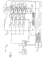
digital controller 400 includes anAC coupler 402, an Analog-to-Digital Converter (ADC) 404,digital oscillators multipliers accumulators gain elements integrators multipliers summation element 430, and Digital-to-Analog Converter (DAC). 432 configured as shown. The AC coupler 402 (e.g., a capacitor) attenuates a high DC voltage measured by theprobe 306 at the surface of the developer. TheADC 404 converts the electrical potential measured by theprobe 306 into a digitized probe signal. Thedigital oscillators accumulators multipliers integrators digital oscillators gain elements integrators summation element 430 receives and adds together the outputs of themultipliers DAC 432 converts the AC correction signal into an analog signal that is provided to the AC power supply (e.g., anHV power supply 434 in this embodiment). - In an example embodiment, the DC controller 170 (FIG. 1) is provided with a digital signal processor (DSP), and elements of the
digital controller 400 are implemented in the DSP. In such an example embodiment, the AC correction value can be provided directly to a DAC of theHV Controller 180. Thus, according to various embodiments, existing ADC, DAC and/or µComputer elements can be utilized to implement the image banding compensation techniques described herein. - In operation, the developer roller probe voltage is Analog-to-Digital converted with a sampling period of Ts. The output from each of the
digital oscillators developer roller 236. Theaccumulators - To drive these Fourier components to zero, the
integrators - The gain of the AC correction loop (Kgain) can be set to null the detected probe signal at a rate much slower than the period of the developer roller itself (Tp). For example, Kgain can be set to zero to disable the nulling action when the probe signal is expected to be inaccurate. In this case, the oscillators will continue to generate the AC correction signal with the same magnitude and phase as when the loop was active (Kgain>0). In an example embodiment, the Fourier sums (Sa1, Ca1) are effectively narrow-band filtered by the accumulator acting as a Fourier summer.
- The AC correction signal is combined with the DC setpoint and converted to an analog signal that is fed to the High Voltage power supply to generate the developer voltage. In an example embodiment, the
HV power supply 434 generates a developer roller bias potential that is proportional to a low voltage input signal supplied by theDAC 432. - Once the AC signal on the developer bias voltage has been adjusted to the correct magnitude and phase to substantially cancel the once-around variation (Tp) in the developer roller, the probe signal will have substantially no signal at this Tp period, the Fourier components Sa1 and Ca1 will be nulled (zero value) and no changes to the As or Bs values will be made. In an example embodiment, the
integrators - Alienation is deactivation of components in the EP process when they are not used. For example, the developer roller in disengaged from the gear drive and the OPC when the engine is shut down or on a color cartridge when mono-only pages are printed. When the cartridge is needed again, the developer roller is re-engaged (De-alienated) but with an arbitrary phase relationship to the previous engagement. After an Alienation-Dealienation cycle, the orientation of the developer relative to the phase of the digital oscillators, ideally, is controlled or available to
digital controller 400. If this is not the case, a lengthier adaptation time can be employed so that the cancellation phase relationship can be re-leamed. - In the example embodiment described above, the
digital controller 400 substantially corrects once-around frequency or first harmonic. Once around nulling provides for a very high rejection of that frequency. In an alterative embodiment, a single digital oscillator can be used instead of two to generate the Sine and Cosine oscillator signals. - In alternative embodiments, additional "banks" of circuitry such as shown in FIG. 4 can be employed in a similar fashion to compensate for other repeatable harmonic components of the developer roller 236 (e.g., twice around, four times around, etc.)
- In an example embodiment, an image forming system includes a photo-conducting surface, a mechanism for selectively charging the photo-conducting surface, a developer including a surface for imparting charged particles to the photo-conducting surface, a mechanism for transferring the charged particles from the photo-conducting surface to an article of media, a mechanism for repositioning the photo-conducting surface in relation to the developer and the article of media, a mechanism for measuring an electrical potential at the surface of the developer, and a mechanism for adjusting an alternating current (AC) component of a developer voltage applied to the developer to correct for image banding caused by variations in the electrical potential. In an example embodiment, the photo-conducting surface, the developer, and the mechanism for measuring are contained within a modular component of the image forming system (such as a printer cartridge).
- By at least reducing or substantially canceling the density variation electronically, the print quality and/or roller manufacturing yield can be increased. Moreover, the cancellation techniques described herein make it easier to accommodate developer rollers from different sub-vendors or different lots from a particular sub-vendor (which can vary significantly), and potentially lessen the benefit that may achieved in using stringent mechanical and/or process control regimes.
- Although embodiments of the present disclosure have been described in terms of the example embodiments above, numerous modifications and/or additions to the above-described embodiments would be readily apparent to one skilled in the art. It is intended that the scope of the claimed subject matter extends to all such modifications and/or additions.
Claims (10)
- An image forming method comprising:measuring an electrical potential on a surface of a developer roller (236); andadjusting a time varying component of a voltage applied to the developer roller (236) using a measurement of the electrical potential.
- The image forming method of claim 1, wherein the time varying component is an alternating current (AC) voltage.
- The image forming method of claim 1, wherein the time varying component is adjusted to reduce a variation in the electrical potential.
- The image forming method of claim 1, wherein the time varying component is adjusted to reduce image banding caused by a variation in the electrical potential.
- The image forming method of claim 1, wherein the time varying component is adjusted to reduce a harmonic component of the electrical potential.
- The image forming method of claim 1, wherein the time varying component is modulated to be out of phase with respect to the electrical potential.
- The image forming method of claim 1, wherein the time varying component is controlled using a digital processing technique.
- The image forming method of claim 1, wherein the time varying component is controlled using one or more digital oscillators.
- The image forming method of claim 1, wherein the time varying component is adjusted to reduce a harmonic component of the electrical potential at a once around frequency of the electrical potential.
- The image forming method of claim 1, wherein the time varying component is adjusted to reduce a higher order harmonic component of the electrical potential.
Applications Claiming Priority (1)
| Application Number | Priority Date | Filing Date | Title |
|---|---|---|---|
| US11/023,215 US7280779B2 (en) | 2004-12-26 | 2004-12-26 | Image banding compensation method |
Publications (1)
| Publication Number | Publication Date |
|---|---|
| EP1675378A2 true EP1675378A2 (en) | 2006-06-28 |
Family
ID=36168475
Family Applications (1)
| Application Number | Title | Priority Date | Filing Date |
|---|---|---|---|
| EP05258044A Withdrawn EP1675378A2 (en) | 2004-12-26 | 2005-12-23 | Image forming method |
Country Status (2)
| Country | Link |
|---|---|
| US (1) | US7280779B2 (en) |
| EP (1) | EP1675378A2 (en) |
Families Citing this family (8)
| Publication number | Priority date | Publication date | Assignee | Title |
|---|---|---|---|---|
| US7937008B2 (en) * | 2007-02-14 | 2011-05-03 | Kyocera Mita Corporation | Image forming apparatus and image forming method |
| US7855806B2 (en) * | 2007-06-27 | 2010-12-21 | Xerox Corporation | Banding profile estimator using multiple sampling intervals |
| US8448336B2 (en) * | 2008-07-03 | 2013-05-28 | Lexmark International, Inc. | Electrophotographic roller with resistance to nip banding |
| US8311463B2 (en) * | 2009-08-18 | 2012-11-13 | Eastman Kodak Company | Method and system to reduce high-frequency banding for electrophotographic development stations |
| US8224209B2 (en) * | 2009-08-18 | 2012-07-17 | Eastman Kodak Company | High-frequency banding reduction for electrophotographic printer |
| US8213816B2 (en) * | 2009-08-27 | 2012-07-03 | Xerox Corporation | Method and system for banding compensation using electrostatic voltmeter based sensing |
| TWI562078B (en) * | 2012-10-04 | 2016-12-11 | Ib Korea Ltd | System and method for mitigating perceived electrical sensation for relief print scanning device and electroluminescent-based relief print scanning device |
| JP6332135B2 (en) * | 2015-05-15 | 2018-05-30 | 京セラドキュメントソリューションズ株式会社 | Image forming apparatus |
Family Cites Families (25)
| Publication number | Priority date | Publication date | Assignee | Title |
|---|---|---|---|---|
| US4420247A (en) * | 1979-12-28 | 1983-12-13 | Canon Kabushiki Kaisha | Computer control means for an electrostatic recording apparatus |
| US4851960A (en) | 1986-12-15 | 1989-07-25 | Canon Kabushiki Kaisha | Charging device |
| JPH0345965A (en) | 1989-07-13 | 1991-02-27 | Mita Ind Co Ltd | Developing device |
| KR970003015B1 (en) * | 1991-07-06 | 1997-03-13 | 후지쓰 가부시끼가이샤 | Developer using one-component developer |
| JPH0627807A (en) | 1992-07-09 | 1994-02-04 | Hiraoka H I Kenkyusho:Kk | Developing device |
| JPH0683179A (en) | 1992-07-13 | 1994-03-25 | Sharp Corp | Electrophotographic device |
| JPH06194944A (en) * | 1992-12-25 | 1994-07-15 | Toshiba Corp | Development device |
| EP0605242B1 (en) | 1992-12-26 | 1997-09-03 | Canon Kabushiki Kaisha | Image forming apparatus having charging member supplied with oscillating voltage |
| JPH06289083A (en) * | 1993-04-01 | 1994-10-18 | Ricoh Co Ltd | Potential measuring apparatus |
| US5815768A (en) | 1997-02-28 | 1998-09-29 | Hewlett-Packard Company | Detection of toner depletion in an electrophotographic printing system |
| JPH11153900A (en) | 1997-09-18 | 1999-06-08 | Ricoh Co Ltd | Image forming device |
| US6266508B1 (en) | 1999-02-25 | 2001-07-24 | Minolta Co., Ltd. | Developing apparatus including an AC voltage applying device |
| JP2001013776A (en) * | 1999-06-29 | 2001-01-19 | Fujitsu Ltd | Toner carrier and image forming apparatus having the same |
| US6101357A (en) | 1999-10-25 | 2000-08-08 | Xerox Corporation | Hybrid scavengeless development using a method for preventing power supply induced banding |
| US6684047B2 (en) * | 2000-04-10 | 2004-01-27 | Seiko Epson Corporation | Image forming apparatus with reduced image defects |
| EP1154332A3 (en) | 2000-05-12 | 2008-09-24 | Seiko Epson Corporation | Developing device |
| JP2002108099A (en) * | 2000-07-28 | 2002-04-10 | Sharp Corp | Developing device |
| US6641244B2 (en) | 2001-11-28 | 2003-11-04 | Hewlett-Packard Development Company, Lp. | Method and apparatus for modifying a printing process in response to environmental conditions received via a network |
| KR100433539B1 (en) | 2002-02-06 | 2004-05-31 | 삼성전자주식회사 | Image formation apparatus compensating the thickness variation of photosensitive body and method of compensating development mass per area |
| KR100467599B1 (en) | 2002-07-24 | 2005-01-24 | 삼성전자주식회사 | Image forming apparatus comprising measurement device of surface voltage and Controling method of development voltage utilizing the same |
| KR100503468B1 (en) | 2002-10-08 | 2005-07-27 | 삼성전자주식회사 | Device for providing high voltage to develope print image of color laser printer |
| JP2004151612A (en) | 2002-11-01 | 2004-05-27 | Seiko Epson Corp | Color image forming equipment |
| JP3944090B2 (en) * | 2003-02-04 | 2007-07-11 | キヤノン株式会社 | Developing device, process cartridge, and image forming apparatus |
| KR100462635B1 (en) * | 2003-03-11 | 2004-12-23 | 삼성전자주식회사 | Electrophotographic image forming apparatus and method of controlling development |
| KR100553911B1 (en) * | 2003-12-19 | 2006-02-24 | 삼성전자주식회사 | High pressure control apparatus and method of image forming apparatus |
-
2004
- 2004-12-26 US US11/023,215 patent/US7280779B2/en not_active Expired - Lifetime
-
2005
- 2005-12-23 EP EP05258044A patent/EP1675378A2/en not_active Withdrawn
Also Published As
| Publication number | Publication date |
|---|---|
| US7280779B2 (en) | 2007-10-09 |
| US20060140655A1 (en) | 2006-06-29 |
Similar Documents
| Publication | Publication Date | Title |
|---|---|---|
| US5710958A (en) | Method for setting up an electrophotographic printing machine using a toner area coverage sensor | |
| US6081678A (en) | Image forming apparatus and method to detect amount of toner adhered to a toner image | |
| GB2331729A (en) | Correcting image density in copiers | |
| US9996037B2 (en) | Image forming apparatus and image forming method which cyclically change a charging power and a developing bias applied to a developer bearer | |
| US5708916A (en) | Developed mass per unit area controller without using electrostatic measurements | |
| JPH10133437A (en) | Image forming device | |
| US5754918A (en) | Electrostatic control with compensation for coupling effects | |
| US20110058184A1 (en) | Least squares based exposure modulation for banding compensation | |
| US7280779B2 (en) | Image banding compensation method | |
| US20160187807A1 (en) | Image forming apparatus | |
| US8269473B2 (en) | AC high voltage power supply device, charging device, developing device, and image forming apparatus | |
| JP5443302B2 (en) | Multi-page coherent analysis using least square method for banding diagnosis compensation in printer | |
| JP5194372B2 (en) | Toner density control device and image forming apparatus | |
| EP1510876B1 (en) | Drive speed control for Image forming apparatus | |
| US8351079B2 (en) | Banding profile estimation using spline interpolation | |
| US6954285B2 (en) | Developing method and developing apparatus featuring two latent image developing operations using two electrical fields | |
| US9268281B2 (en) | Image forming apparatus | |
| JP6628132B2 (en) | Image forming device | |
| KR100400000B1 (en) | Controlling apparatus of optical density for liquid electrophotographic printer and the controlling method thereof | |
| EP0519710B1 (en) | Image forming apparatus having image forming condition controller responsive to test pattern image | |
| JP7010134B2 (en) | Image forming device and image forming method | |
| JP2010048960A (en) | Image forming apparatus | |
| JP2009042432A (en) | Image forming apparatus | |
| JP3072806B2 (en) | Image forming device | |
| JP6900679B2 (en) | Image forming device and correction method |
Legal Events
| Date | Code | Title | Description |
|---|---|---|---|
| PUAI | Public reference made under article 153(3) epc to a published international application that has entered the european phase |
Free format text: ORIGINAL CODE: 0009012 |
|
| AK | Designated contracting states |
Kind code of ref document: A2 Designated state(s): AT BE BG CH CY CZ DE DK EE ES FI FR GB GR HU IE IS IT LI LT LU LV MC NL PL PT RO SE SI SK TR |
|
| AX | Request for extension of the european patent |
Extension state: AL BA HR MK YU |
|
| STAA | Information on the status of an ep patent application or granted ep patent |
Free format text: STATUS: THE APPLICATION HAS BEEN WITHDRAWN |
|
| 18W | Application withdrawn |
Effective date: 20080507 |