EP1675261A1 - Surface acoustic wave device and method of manufacturing a surface acoustic wave device - Google Patents
Surface acoustic wave device and method of manufacturing a surface acoustic wave device Download PDFInfo
- Publication number
- EP1675261A1 EP1675261A1 EP20050027864 EP05027864A EP1675261A1 EP 1675261 A1 EP1675261 A1 EP 1675261A1 EP 20050027864 EP20050027864 EP 20050027864 EP 05027864 A EP05027864 A EP 05027864A EP 1675261 A1 EP1675261 A1 EP 1675261A1
- Authority
- EP
- European Patent Office
- Prior art keywords
- acoustic wave
- surface acoustic
- wiring
- insulating film
- region
- Prior art date
- Legal status (The legal status is an assumption and is not a legal conclusion. Google has not performed a legal analysis and makes no representation as to the accuracy of the status listed.)
- Granted
Links
- 238000010897 surface acoustic wave method Methods 0.000 title claims abstract description 183
- 238000004519 manufacturing process Methods 0.000 title claims description 20
- 239000010408 film Substances 0.000 claims abstract description 154
- 239000004065 semiconductor Substances 0.000 claims abstract description 73
- 239000000758 substrate Substances 0.000 claims abstract description 30
- 239000010409 thin film Substances 0.000 claims abstract description 22
- 238000000034 method Methods 0.000 description 12
- VYPSYNLAJGMNEJ-UHFFFAOYSA-N Silicium dioxide Chemical compound O=[Si]=O VYPSYNLAJGMNEJ-UHFFFAOYSA-N 0.000 description 8
- 229910052681 coesite Inorganic materials 0.000 description 4
- 229910052906 cristobalite Inorganic materials 0.000 description 4
- 239000000377 silicon dioxide Substances 0.000 description 4
- 229910052682 stishovite Inorganic materials 0.000 description 4
- 229910052905 tridymite Inorganic materials 0.000 description 4
- 239000000463 material Substances 0.000 description 3
- 229910052710 silicon Inorganic materials 0.000 description 3
- 239000010703 silicon Substances 0.000 description 3
- 229910052581 Si3N4 Inorganic materials 0.000 description 2
- 239000011521 glass Substances 0.000 description 2
- 238000004528 spin coating Methods 0.000 description 2
- 229910001218 Gallium arsenide Inorganic materials 0.000 description 1
- 229910020328 SiSn Inorganic materials 0.000 description 1
- 229910000577 Silicon-germanium Inorganic materials 0.000 description 1
- -1 as shown in Fig. 5A Substances 0.000 description 1
- 238000005530 etching Methods 0.000 description 1
- 229910052949 galena Inorganic materials 0.000 description 1
- 229910003465 moissanite Inorganic materials 0.000 description 1
- 238000005498 polishing Methods 0.000 description 1
- 235000019353 potassium silicate Nutrition 0.000 description 1
- SBIBMFFZSBJNJF-UHFFFAOYSA-N selenium;zinc Chemical compound [Se]=[Zn] SBIBMFFZSBJNJF-UHFFFAOYSA-N 0.000 description 1
- 229910010271 silicon carbide Inorganic materials 0.000 description 1
- 239000000126 substance Substances 0.000 description 1
- 239000012808 vapor phase Substances 0.000 description 1
Images



Classifications
-
- H—ELECTRICITY
- H03—ELECTRONIC CIRCUITRY
- H03H—IMPEDANCE NETWORKS, e.g. RESONANT CIRCUITS; RESONATORS
- H03H9/00—Networks comprising electromechanical or electro-acoustic elements; Electromechanical resonators
- H03H9/02—Details
- H03H9/125—Driving means, e.g. electrodes, coils
- H03H9/145—Driving means, e.g. electrodes, coils for networks using surface acoustic waves
-
- H—ELECTRICITY
- H03—ELECTRONIC CIRCUITRY
- H03H—IMPEDANCE NETWORKS, e.g. RESONANT CIRCUITS; RESONATORS
- H03H3/00—Apparatus or processes specially adapted for the manufacture of impedance networks, resonating circuits, resonators
- H03H3/007—Apparatus or processes specially adapted for the manufacture of impedance networks, resonating circuits, resonators for the manufacture of electromechanical resonators or networks
- H03H3/08—Apparatus or processes specially adapted for the manufacture of impedance networks, resonating circuits, resonators for the manufacture of electromechanical resonators or networks for the manufacture of resonators or networks using surface acoustic waves
-
- H—ELECTRICITY
- H03—ELECTRONIC CIRCUITRY
- H03H—IMPEDANCE NETWORKS, e.g. RESONANT CIRCUITS; RESONATORS
- H03H9/00—Networks comprising electromechanical or electro-acoustic elements; Electromechanical resonators
- H03H9/02—Details
- H03H9/02535—Details of surface acoustic wave devices
- H03H9/02818—Means for compensation or elimination of undesirable effects
- H03H9/02866—Means for compensation or elimination of undesirable effects of bulk wave excitation and reflections
-
- H—ELECTRICITY
- H03—ELECTRONIC CIRCUITRY
- H03H—IMPEDANCE NETWORKS, e.g. RESONANT CIRCUITS; RESONATORS
- H03H9/00—Networks comprising electromechanical or electro-acoustic elements; Electromechanical resonators
- H03H9/02—Details
- H03H9/02535—Details of surface acoustic wave devices
- H03H9/0296—Surface acoustic wave [SAW] devices having both acoustic and non-acoustic properties
- H03H9/02976—Surface acoustic wave [SAW] devices having both acoustic and non-acoustic properties with semiconductor devices
Definitions
- the present invention relates to a surface acoustic wave device provided with an IC region and a surface acoustic wave element region on a semiconductor substrate to form a single chip.
- SAW resonator or a SAW filter have various superior characteristics such as high frequency, compact size, or high mass productivity, and therefore, are widely used in the telecommunications field.
- SAW resonator or a SAW filter have various superior characteristics such as high frequency, compact size, or high mass productivity, and therefore, are widely used in the telecommunications field.
- downsizing and weight saving of components used in the high-frequency area are strongly desired.
- a surface acoustic wave device having a SAW filter formed by providing a piezoelectric thin film on a semiconductor substrate partially provided with a high-frequency amplifier circuit or the like instead of using a surface acoustic wave element as a filter unit.
- semiconductor elements and wiring for connecting the semiconductor elements are formed via an insulating film as a multi-layered structure in the IC region. Since, in contrast, only the insulating film is stacked in the surface acoustic wave element region, a step is created between the IC region and the surface acoustic wave element region.
- a large number of surface acoustic wave devices are formed in a semiconductor wafer so as to border on each other, and as layers such as the insulating layer are stacked, the step inclines and advances to the surface acoustic wave element region, this causes a problem that the flatness of the surface of the surface acoustic wave element region cannot be assured. If the flatness of the surface is not sufficient, the surface acoustic wave element cannot be manufactured with sufficient dimensional accuracy, which degrades the performance of the surface acoustic wave element. Further, the unevenness of the surface caused by the insufficient flatness causes a variation in the thickness of the piezoelectric thin film formed thereon, and a variation in the resonant frequency of the surface acoustic wave element is concerned.
- an advantage of the present invention is to provide a surface acoustic wave device, which is equipped with an IC region and a surface acoustic wave element region in a semiconductor substrate and is configured as a single chip, and a method of manufacturing the surface acoustic wave device capable of ensuring evenness of the surface acoustic wave element region, and thus obtaining superior characteristics.
- a surface acoustic wave device includes at least an IC region and a surface acoustic wave element region in a semiconductor substrate and is formed as a single chip, and includes in the IC region a semiconductor element layer having a semiconductor element and an element insulating film formed to cover the semiconductor element and extending to the surface acoustic wave element region, a wiring layer formed by stacking, on the semiconductor element layer, wiring for establishing connection with the semiconductor element and a wiring insulating film extending to the surface acoustic wave element region and for insulating the wiring, a piezoelectric thin film formed above the wiring insulating film.
- the surface acoustic wave device further includes, in the surface acoustic wave element region, a surface acoustic wave element formed on the piezoelectric thin film and equipped with an IDT electrode provided with a plurality of electrode fingers, and at least one layer of layer thickness adjusting films having linear shapes and arranged in parallel to the electrode fingers of the IDT electrode and with the same pitch as the electrode fingers of the IDT electrode.
- the layer thickness adjusting films are formed above the semiconductor substrate, the element insulating film, or the wiring insulating film, and below an area in which the surface acoustic wave element is formed.
- the step between the IC region and the surface acoustic wave element region can be reduced by providing the layer thickness adjusting films on the semiconductor substrate, the element insulating film, or the wiring insulating film in the surface acoustic wave element region, thus evenness of the surface acoustic wave element region can be ensured. Further, the diffused reflection of the surface acoustic wave excited by the IDT electrodes can be prevented by providing the layer thickness adjusting films having linear shapes substantially in parallel to and with the same pitch as the electrode fingers of the IDT electrodes.
- the surface acoustic wave element can be formed in the even surface acoustic wave element region to form the IDT electrodes with good dimensional accuracy to reduce variation in the resonant frequency of the surface acoustic wave element, and further to prevent the diffused reflection of the surface acoustic wave, thus the surface acoustic wave device with superior characteristics can be provided.
- the layer thickness adjusting films are formed in the same pitch as the pitch of the electrode fingers with respect to positions where the center lines of the electrode fingers in the line width direction match the respective center lines of the layer thickness adjusting films in the line width direction. According to this configuration, the diffused reflection of the surface acoustic wave can effectively be prevented, thus providing the surface acoustic wave element with good characteristics.
- the width of each of the electrode fingers is equal to the width of respective one of the layer thickness adjusting films. According to this configuration, the diffused reflection of the surface acoustic wave can further effectively be prevented, thus providing the surface acoustic wave element with good characteristics.
- each of the layer thickness adjusting films has a shape composed of discontinuous lines. According to this configuration, the layer thickness adjusting films can more easily be formed, and freedom of designing the layer thickness adjusting films can be increased.
- the surface acoustic wave device further includes a moisture resistant film between the wiring insulating film and the piezoelectric thin film. According to this configuration, the IC can be protected form an influence of moisture, thus providing the surface acoustic wave device with high reliability.
- a method of manufacturing a surface acoustic wave device includes the steps of (a) forming in the IC region of the semiconductor substrate a semiconductor element layer, the step (a) including the steps of (a1) providing a semiconductor element and (a2) providing an element insulating film covering the semiconductor element, (b) forming on the semiconductor element layer a wiring layer, the step (b) including the steps of (b1) providing wiring for establishing connection with the semiconductor element and (b2) providing a wiring insulating film for insulating the wiring stacked on the wiring.
- the step (a2) includes the step of forming in the surface acoustic wave element region the element insulating film composing the semiconductor element layer
- the step (b2) includes the step of forming in the surface acoustic wave element region the wiring insulating film composing the wiring layer in a stacked manner.
- the method further includes the steps of (c) forming a piezoelectric thin film above the wiring insulating film in the surface acoustic wave element region, (d) forming a surface acoustic wave element on the piezoelectric thin film in the surface acoustic wave element region, and (e) forming at least one layer of layer thickness adjusting films having linear shapes and arranged in parallel to and with the same pitch as electrode fingers of an IDT electrode above one of the semiconductor substrate, the element insulating film, and the wiring insulating film, and below an area in which the surface acoustic wave element is formed.
- the step between the IC region and the surface acoustic wave element region can be reduced by providing the layer thickness adjusting films on the semiconductor substrate, the element insulating film, or the wiring insulating film in the surface acoustic wave element region, thus evenness of the surface acoustic wave element region can be ensured. Further, the diffused reflection of the surface acoustic wave excited by the IDT electrodes can be prevented by providing the layer thickness adjusting films having linear shapes substantially in parallel to and with the same pitch as the electrode fingers of the IDT electrodes.
- the surface acoustic wave element can be formed in the even surface acoustic wave element region to form the IDT electrodes with good dimensional accuracy to reduce variation in the resonant frequency of the surface acoustic wave element, and further to prevent the diffused reflection of the surface acoustic wave, thus the method of manufacturing the surface acoustic wave device with superior characteristics can be provided.
- the step (b1) and the step (e) are executed simultaneously to form the layer thickness adjusting films with the wiring in the same layer.
- the layer thickness adjusting films can be formed with the wiring in the IC region in the common process, thus the layer thickness adjusting films can efficiently be formed.
- the method of manufacturing the surface acoustic wave device further includes the step of forming a moisture resistant film between the wiring insulating film and the piezoelectric thin film.
- the IC can be protected form an influence of moisture, thus providing the method of manufacturing the surface acoustic wave device with high reliability.
- Fig. 1 is a schematic plan view showing a surface acoustic wave device according to an embodiment of the invention.
- Fig. 2 is a schematic partial cross-sectional view of the surface acoustic wave device.
- Fig. 3 is a schematic partial cross-sectional view of the surface acoustic wave device.
- Fig. 4 is a schematic plan view showing a layout pattern of a set of layer thickness adjusting films.
- Figs. 5A and 5B are schematic plan views each showing a layout pattern of another set of the layer thickness adjusting films.
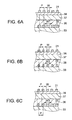
- Figs. 6A through 6C are schematic partial cross-sectional views each showing the positional relationship between another surface acoustic wave element and the layer thickness adjusting films.
- Figs. 7A through 7D are schematic cross-sectional views for explaining a method of manufacturing the surface acoustic wave device.
- Fig. 1 is a schematic plan view showing a surface acoustic wave device according to an embodiment of the invention.
- a surface acoustic wave device 1 is provided with an IC region 10 and a surface acoustic wave element region 20 in a semiconductor substrate.
- a semiconductor element shown in Fig. 2 is formed on the semiconductor substrate, and Al wiring 11 for connecting the semiconductor element is stacked thereon.
- Al pads 12 are provided for electrical connection with the outside.
- a high-frequency circuit such as an oscillator circuit for driving the surface acoustic wave element 24 is included in the IC region 10.
- the semiconductor substrate is equipped with the IC region 10 and the surface acoustic wave element region 20 to configure the surface acoustic wave device 1 as a single chip.
- Fig. 2 is a schematic partial cross-sectional view along the A-A line in the surface acoustic wave device 1 shown in Fig. 1.
- the IC region 10 on the semiconductor substrate 30 made of silicon there are formed a large number of semiconductor elements 31 using a known method.
- the surface acoustic wave element region 20 on the semiconductor substrate 30 there is formed first layer thickness adjusting films 32 made of Al.
- an element insulating film 33 made of SiO 2 is formed on the semiconductor elements 31 and the first layer thickness adjusting films 32 to insulate the semiconductor elements 31.
- a semiconductor element layer 40 composed of the semiconductor elements 31 and the element insulating film 33 is formed in the IC region 10.
- the element insulating film 33 in the IC region 10 there is formed Al wiring 11 for connecting the semiconductor 31, and on the element insulating film 33 in the surface acoustic wave element region 20, there are formed second layer thickness adjusting films 35.
- the second layer thickness adjusting films 35 are provided using the same processes as the Al wiring 11, and are formed to have the same thickness as the Al wiring 11.
- a wiring insulating film 36 made of SiO 2 is formed on the Al wiring 11.
- a wiring layer 41 composed of the A1 wiring 11 and the wiring insulating film 36 is formed in the IC region 10.
- a moisture resistant film 37 made of Si 3 N 4 is formed on the wiring insulating film 36, and a piezoelectric thin film 38 made of ZnO is formed on the moisture resistant film 37. Further, on the piezoelectric thin film 38 in the surface acoustic wave element 20, there is formed a surface acoustic wave element 24 made of Al.
- Fig. 3 is a schematic cross-sectional view along the B-B cutting line in Fig. 1
- Fig. 4 is a schematic plan view for showing a layout pattern of a set of the layer thickness adjusting films.
- the first layer thickness adjusting films 32 formed on the semiconductor substrate 30 are disposed on the surface acoustic wave element region 20, for example.
- the first layer thickness adjusting films 32 are formed linearly and substantially in parallel to the electrode fingers of the IDT electrode.
- the second layer thickness adjusting films 35 are also disposed in the same shape as described above.
- the IDT electrodes 22 are equipped with the electrode fingers 21, and the electrode fingers 21 are formed in series with a pitch P. Further, electrodes 26 of the reflectors 23 are also formed in the pitch P, thus forming the surface acoustic wave element 24 to have the shape having the electrodes aligned in series with the pitch P. And, the electrode fingers 21 and the electrodes 26 of the reflectors 23 are formed to have the same line width W.
- the first layer thickness adjusting films 32 and the second layer thickness adjusting films 35 are formed to have the same pitch P as that of the electrode fingers 21 with respect to the positions having the same center lines of the respective electrode fingers 21 in the width direction. Further, the width W of each of the first layer thickness adjusting films 32 and the second layer thickness adjusting films 35 is formed to be the same as the width W of each of the electrode fingers 21. Note that, the area in which the first layer thickness adjusting films 32 and the second layer thickness adjusting films 35 are formed is formed to be equal to or wider than the area in which the surface acoustic wave element 24 is formed.
- the step between the IC region 10 with the multi-layered structure and the surface acoustic wave element region 20 can be reduced by appropriately forming the layer thickness adjusting films having the same shapes as described above on the wiring insulating film.
- the step between the IC region 10 and the surface acoustic wave element region 20 can be reduced.
- the step inclines and advances to the surface acoustic wave element region 20 while the layers such as an insulating layer are stacked in the surface acoustic wave element region 20, thus ensuring evenness of the surface acoustic wave element region 20.
- the surface acoustic wave element 24 can be formed with high dimensional accuracy in the surface acoustic wave element region 20 whose evenness is ensured, thus the surface acoustic wave element 24 having superior characteristics can be obtained.
- the layer thickness adjusting films are provided so as to traverse the electrode fingers 21 of the IDT electrodes 22, interference or scattering is caused in the surface acoustic wave to attenuate the surface acoustic wave, thus making it difficult to obtain the superior characteristics. Therefore, in the present embodiment, diffused reflection of the surface acoustic wave proceeding in the depth direction can be prevented by providing the first layer thickness adjusting films 32 and the second layer thickness adjusting films 35 substantially in parallel to the electrode fingers 21 of the IDT electrodes 22 with the same pitch.
- the surface acoustic wave element 24 having superior characteristics can be formed, thus providing the surface acoustic wave device 1 having superior characteristics.
- Figs. 5A and 5B are schematic plan views each showing a modified example of the layout pattern of the set of the layer thickness adjusting films.
- layer thickness adjusting film 50 formed as a pattern composed of discontinuous lines can also be adopted.
- the first layer thickness adjusting films 50 to be formed in the surface acoustic wave element region 20 of the semiconductor substrate 30 are formed so that each of the layer thickness adjusting films is divided into pieces.
- the interval sections are preferably formed so that each of the interval sections is not continued to another one of the interval sections of the adjacent layer thickness adjusting film. According to this arrangement, the layer thickness adjusting films can more easily be formed, and freedom of designing the layer thickness adjusting films can be increased.
- layer thickness adjusting films 51 having the same pattern as the surface acoustic wave element can also be adopted.
- the photo mask used for forming the surface acoustic wave element can be shared.
- Figs. 6A through 6C are schematic partial cross-sectional views each showing a modified example of the line width of the layer thickness adjusting films and the positional relationship with the surface acoustic wave element.
- the layer thickness adjusting films can be formed to have the line width W1 wider than the line width W of the electrode fingers 21.
- the second layer thickness adjusting films 35 are formed in the same pitch P as the electrode fingers 21 with respect to the positions having the same center lines as the electrode fingers 21 in the direction of the width W, and the layer thickness adjusting films are formed to have the line width W1 wider than the line width W of the electrode fingers 21.
- the layer thickness adjusting films can be formed to have the line width W2 narrower than the line width W of the electrode fingers 21.
- the second layer thickness adjusting films 35 are formed in the same pitch P as the electrode fingers 21 with respect to the positions having the same center lines as the electrode fingers 21 in the direction of the width W, and the layer thickness adjusting films are formed to have the line width W2 narrower than the line width W of the electrode fingers 21.
- the layer thickness adjusting films can also be formed to have the same pitch P as the electrode fingers 21, different center lines from those of the electrode fingers 21 in the direction of the width W, and the line width W3 including the line width W of the electrode fingers 21.
- the second layer thickness adjusting films 35 are formed with the same pitch P as the electrode fingers 21, and the layer thickness adjusting films 35 having the width W3 are disposed in the positions including the respective electrode fingers 21 and have different center lines from those of the electrode fingers 21 in the direction of the width W. Therefore, the layer thickness adjusting films 35 are formed to have the width W3 wider than the width W of the electrode fingers 21.
- the structure described above can commonly be adopted to the first layer thickness adjusting films, and the surface acoustic wave proceeding to the depth of about one wavelength can be prevented from being diffusely reflected.
- the present embodiment is described taking the case provided with the moisture resistant film 37 as an example, it can be implemented without the moisture resistant film 37 depending on the package or the use environment of the surface acoustic wave device 1.
- a CMP (Chemical Mechanical Polishing) process can be executed after forming the wiring insulating film 36 or the moisture resistant film 37 to obtain evenness with better precision.
- the evenness with good precision can also be obtained by using glass coated by a spin-coating process (Spin On Glass (hereinafter referred to as SOG)) as the element insulating film 33.
- the surface acoustic wave element 24 can be electromagnetically shielded.
- FIGs. 7A through 7D are views for explaining processes showing a method of manufacturing the surface acoustic wave device according to an embodiment of the invention, and the processes proceed in the order from 7A to 7D.
- a large number of semiconductor elements 31 are formed in the IC region 10 on the semiconductor substrate 30 made of silicon.
- the first layer thickness adjusting films 32 made of Al are formed in the surface acoustic wave element region 20 on the semiconductor substrate 30.
- the first layer thickness adjusting films 32 are formed linearly and substantially in parallel to the electrode fingers of the IDT electrode of the surface acoustic wave element, as shown in Fig. 4. Further, the first layer thickness adjusting films 32 are formed to have the same pitch and the same line width as the electrode fingers of the IDT electrode.
- the element insulating film 33 made of SiO 2 is formed on the semiconductor substrate 30 to insulate the semiconductor element 31.
- the element insulating film 33 is formed not only in the IC region 10 but also in the surface acoustic wave element region 20.
- a semiconductor element layer 40 composed of the semiconductor elements 31 and the element insulating film 33 is formed in the IC region 10.
- a part of the element insulating film 33 on the semiconductor element 31 in the IC region 10 is removed by etching to form an opening, and then the opening is filled with A1 to form the Al wiring 11 electrically connected to the semiconductor element 31.
- the second layer thickness adjusting films 35 are formed in the surface acoustic wave element region 20 together with the Al wiring 11.
- the second layer thickness adjusting films 35 are formed linearly and substantially in parallel to the electrode fingers of the IDT electrode of the surface acoustic wave element, similarly to the first layer thickness adjusting films 32.
- the wiring insulating film 36 made of SiO 2 is formed in both the IC region 10 and the surface acoustic wave element region 20 to insulate the Al wiring 11.
- a wiring layer 41 composed of the Al wiring 11 and the wiring insulating film 36 is formed in the IC region 10.
- the moisture resistant film 37 made of Si 3 N 4 is formed in both the IC region 10 and the surface acoustic wave element region 20, thus moisture resistant property of the IC can be enhanced.
- the piezoelectric thin film 38 made of ZnO is formed on the moisture resistant film 37 in both the IC region 10 and the surface acoustic wave element region 20.
- the surface acoustic wave element 24 is formed on the piezoelectric thin film 38 in the surface acoustic wave element region 20.
- the surface acoustic wave element 24 is formed as a SAW resonator equipped with the IDT electrodes 22 and the reflectors 23 shown in Fig. 1.
- the semiconductor substrate 30 is equipped with the IC region 10 and the surface acoustic wave element region 20, thus the surface acoustic wave device 1 configured as a single chip can be obtained.
- the step between the IC region 10 with the multi-layered structure and the surface acoustic wave element region 20 can be reduced by appropriately forming the layer thickness adjusting films having the same shapes as described above on the wiring insulating film.
- the layout pattern of the layer thickness adjusting films the layout patterns described in the modified examples of the first embodiment can also be provided.
- the step between the IC region 10 and the surface acoustic wave element region 20 can be reduced.
- the surface acoustic wave element 24 can be formed with high dimensional accuracy in the surface acoustic wave element region 20 whose evenness is ensured, thus the surface acoustic wave element 24 having superior characteristics can be obtained.
- the surface acoustic wave excited by the IDT electrodes 22 proceeds to the depth of about one wavelength, the surface acoustic wave proceeding in the depth direction can be prevented from being diffusely reflected by providing the first layer thickness adjusting films 32 and the second layer thickness adjusting films 35 in the same pitch as the electrode fingers 21 of the IDT electrodes 22.
- the surface acoustic wave element 24 having superior characteristics can be formed, thus making it possible to provide the surface acoustic wave device 1 having superior characteristics.
- the element insulating film 33 shown in Fig. 2 or Fig. 7B is often formed using a vapor phase process in response to a higher frequency or finer pitch wiring.
- the previous-generation wiring of no smaller than 0.35 ⁇ m can be adopted.
- SOG SOG
- liquid glass is deposited on a wafer by spin-coating in a preliminary rotational speed of 300rpm for 3 seconds, and then in a main rotational speed of 3000rpm for 10 seconds. After then, it is processed in a baking oven at 80°C for 3 minutes, and finally cured at 300°C for 60 minutes to be completed.
- the surface acoustic wave element 24 having superior characteristics can be formed, thus making it possible to provide the surface acoustic wave device 1 having superior characteristics at a low price.
Landscapes
- Physics & Mathematics (AREA)
- Acoustics & Sound (AREA)
- Engineering & Computer Science (AREA)
- Manufacturing & Machinery (AREA)
- Surface Acoustic Wave Elements And Circuit Networks Thereof (AREA)
Abstract

Description
- The present invention relates to a surface acoustic wave device provided with an IC region and a surface acoustic wave element region on a semiconductor substrate to form a single chip.
- Surface acoustic wave devices represented by a SAW resonator or a SAW filter have various superior characteristics such as high frequency, compact size, or high mass productivity, and therefore, are widely used in the telecommunications field. In recent years, along with the popularization of mobile telecommunication devices, downsizing and weight saving of components used in the high-frequency area are strongly desired.
- To cope with the desire, as shown in a document of J. H. Viseer, IEEE, Ultrasonics Symposium, p.195-200 (1989), for example, there is proposed a surface acoustic wave device having a SAW filter formed by providing a piezoelectric thin film on a semiconductor substrate partially provided with a high-frequency amplifier circuit or the like instead of using a surface acoustic wave element as a filter unit.
- In such a surface acoustic wave device equipped with an IC region and a surface acoustic wave region on a semiconductor substrate to form a single chip, semiconductor elements and wiring for connecting the semiconductor elements are formed via an insulating film as a multi-layered structure in the IC region. Since, in contrast, only the insulating film is stacked in the surface acoustic wave element region, a step is created between the IC region and the surface acoustic wave element region. Typically, in case of such a surface acoustic wave device, a large number of surface acoustic wave devices are formed in a semiconductor wafer so as to border on each other, and as layers such as the insulating layer are stacked, the step inclines and advances to the surface acoustic wave element region, this causes a problem that the flatness of the surface of the surface acoustic wave element region cannot be assured. If the flatness of the surface is not sufficient, the surface acoustic wave element cannot be manufactured with sufficient dimensional accuracy, which degrades the performance of the surface acoustic wave element. Further, the unevenness of the surface caused by the insufficient flatness causes a variation in the thickness of the piezoelectric thin film formed thereon, and a variation in the resonant frequency of the surface acoustic wave element is concerned.
- In view of the above technical background, an advantage of the present invention is to provide a surface acoustic wave device, which is equipped with an IC region and a surface acoustic wave element region in a semiconductor substrate and is configured as a single chip, and a method of manufacturing the surface acoustic wave device capable of ensuring evenness of the surface acoustic wave element region, and thus obtaining superior characteristics.
- A surface acoustic wave device according to an aspect of the invention includes at least an IC region and a surface acoustic wave element region in a semiconductor substrate and is formed as a single chip, and includes in the IC region a semiconductor element layer having a semiconductor element and an element insulating film formed to cover the semiconductor element and extending to the surface acoustic wave element region, a wiring layer formed by stacking, on the semiconductor element layer, wiring for establishing connection with the semiconductor element and a wiring insulating film extending to the surface acoustic wave element region and for insulating the wiring, a piezoelectric thin film formed above the wiring insulating film. And the surface acoustic wave device further includes, in the surface acoustic wave element region, a surface acoustic wave element formed on the piezoelectric thin film and equipped with an IDT electrode provided with a plurality of electrode fingers, and at least one layer of layer thickness adjusting films having linear shapes and arranged in parallel to the electrode fingers of the IDT electrode and with the same pitch as the electrode fingers of the IDT electrode. The layer thickness adjusting films are formed above the semiconductor substrate, the element insulating film, or the wiring insulating film, and below an area in which the surface acoustic wave element is formed.
- According to this configuration, the step between the IC region and the surface acoustic wave element region can be reduced by providing the layer thickness adjusting films on the semiconductor substrate, the element insulating film, or the wiring insulating film in the surface acoustic wave element region, thus evenness of the surface acoustic wave element region can be ensured. Further, the diffused reflection of the surface acoustic wave excited by the IDT electrodes can be prevented by providing the layer thickness adjusting films having linear shapes substantially in parallel to and with the same pitch as the electrode fingers of the IDT electrodes.
- As described above, the surface acoustic wave element can be formed in the even surface acoustic wave element region to form the IDT electrodes with good dimensional accuracy to reduce variation in the resonant frequency of the surface acoustic wave element, and further to prevent the diffused reflection of the surface acoustic wave, thus the surface acoustic wave device with superior characteristics can be provided.
- In the surface acoustic wave device according to another aspect of the invention, the layer thickness adjusting films are formed in the same pitch as the pitch of the electrode fingers with respect to positions where the center lines of the electrode fingers in the line width direction match the respective center lines of the layer thickness adjusting films in the line width direction. According to this configuration, the diffused reflection of the surface acoustic wave can effectively be prevented, thus providing the surface acoustic wave element with good characteristics.
- In the surface acoustic wave device according to still another aspect of the invention, the width of each of the electrode fingers is equal to the width of respective one of the layer thickness adjusting films. According to this configuration, the diffused reflection of the surface acoustic wave can further effectively be prevented, thus providing the surface acoustic wave element with good characteristics.
- In the surface acoustic wave device according to another aspect of the invention, each of the layer thickness adjusting films has a shape composed of discontinuous lines. According to this configuration, the layer thickness adjusting films can more easily be formed, and freedom of designing the layer thickness adjusting films can be increased.
- The surface acoustic wave device according to still another aspect of the invention further includes a moisture resistant film between the wiring insulating film and the piezoelectric thin film. According to this configuration, the IC can be protected form an influence of moisture, thus providing the surface acoustic wave device with high reliability.
- A method of manufacturing a surface acoustic wave device according to another aspect of the invention, the surface acoustic wave device including at least an IC region and a surface acoustic wave element region in a semiconductor substrate and formed as a single chip, includes the steps of (a) forming in the IC region of the semiconductor substrate a semiconductor element layer, the step (a) including the steps of (a1) providing a semiconductor element and (a2) providing an element insulating film covering the semiconductor element, (b) forming on the semiconductor element layer a wiring layer, the step (b) including the steps of (b1) providing wiring for establishing connection with the semiconductor element and (b2) providing a wiring insulating film for insulating the wiring stacked on the wiring. In this case, the step (a2) includes the step of forming in the surface acoustic wave element region the element insulating film composing the semiconductor element layer, and the step (b2) includes the step of forming in the surface acoustic wave element region the wiring insulating film composing the wiring layer in a stacked manner. The method further includes the steps of (c) forming a piezoelectric thin film above the wiring insulating film in the surface acoustic wave element region, (d) forming a surface acoustic wave element on the piezoelectric thin film in the surface acoustic wave element region, and (e) forming at least one layer of layer thickness adjusting films having linear shapes and arranged in parallel to and with the same pitch as electrode fingers of an IDT electrode above one of the semiconductor substrate, the element insulating film, and the wiring insulating film, and below an area in which the surface acoustic wave element is formed.
- According to this method of manufacturing a surface acoustic wave device, the step between the IC region and the surface acoustic wave element region can be reduced by providing the layer thickness adjusting films on the semiconductor substrate, the element insulating film, or the wiring insulating film in the surface acoustic wave element region, thus evenness of the surface acoustic wave element region can be ensured. Further, the diffused reflection of the surface acoustic wave excited by the IDT electrodes can be prevented by providing the layer thickness adjusting films having linear shapes substantially in parallel to and with the same pitch as the electrode fingers of the IDT electrodes.
- As described above, the surface acoustic wave element can be formed in the even surface acoustic wave element region to form the IDT electrodes with good dimensional accuracy to reduce variation in the resonant frequency of the surface acoustic wave element, and further to prevent the diffused reflection of the surface acoustic wave, thus the method of manufacturing the surface acoustic wave device with superior characteristics can be provided.
- In the method of manufacturing a surface acoustic wave device according to still another aspect of the invention, the step (b1) and the step (e) are executed simultaneously to form the layer thickness adjusting films with the wiring in the same layer.
- According to this method of manufacturing the surface acoustic wave device, the layer thickness adjusting films can be formed with the wiring in the IC region in the common process, thus the layer thickness adjusting films can efficiently be formed.
- The method of manufacturing the surface acoustic wave device according to still another aspect of the invention further includes the step of forming a moisture resistant film between the wiring insulating film and the piezoelectric thin film.
- According to this method of manufacturing the surface acoustic wave device, the IC can be protected form an influence of moisture, thus providing the method of manufacturing the surface acoustic wave device with high reliability.
- The invention will now be described with reference to the accompanying drawings, wherein like numbers refer to like elements.
- Fig. 1 is a schematic plan view showing a surface acoustic wave device according to an embodiment of the invention.
- Fig. 2 is a schematic partial cross-sectional view of the surface acoustic wave device.
- Fig. 3 is a schematic partial cross-sectional view of the surface acoustic wave device.
- Fig. 4 is a schematic plan view showing a layout pattern of a set of layer thickness adjusting films.
- Figs. 5A and 5B are schematic plan views each showing a layout pattern of another set of the layer thickness adjusting films.
- Figs. 6A through 6C are schematic partial cross-sectional views each showing the positional relationship between another surface acoustic wave element and the layer thickness adjusting films.
- Figs. 7A through 7D are schematic cross-sectional views for explaining a method of manufacturing the surface acoustic wave device.
- Hereinafter, embodiments of the invention will be described with reference to the accompanying drawings.
- First Embodiment
- Fig. 1 is a schematic plan view showing a surface acoustic wave device according to an embodiment of the invention. A surface
acoustic wave device 1 is provided with anIC region 10 and a surface acousticwave element region 20 in a semiconductor substrate. In the IC region, a semiconductor element (shown in Fig. 2) is formed on the semiconductor substrate, andAl wiring 11 for connecting the semiconductor element is stacked thereon. And,Al pads 12 are provided for electrical connection with the outside. Further, a high-frequency circuit such as an oscillator circuit for driving the surfaceacoustic wave element 24 is included in theIC region 10. - In the surface acoustic
wave element region 20, there is formed a SAW resonator as the surfaceacoustic wave element 24 equipped withIDT electrodes 22 andreflectors 23. TheIDT electrodes 22 are equipped withelectrode fingers 21 disposed so as to alternately engage with each other. And,Al pads 25 are provided for electrical connection with the outside. As described above, the semiconductor substrate is equipped with theIC region 10 and the surface acousticwave element region 20 to configure the surfaceacoustic wave device 1 as a single chip. - Fig. 2 is a schematic partial cross-sectional view along the A-A line in the surface
acoustic wave device 1 shown in Fig. 1. In theIC region 10 on thesemiconductor substrate 30 made of silicon, there are formed a large number ofsemiconductor elements 31 using a known method. Further, in the surface acousticwave element region 20 on thesemiconductor substrate 30, there is formed first layerthickness adjusting films 32 made of Al. And, anelement insulating film 33 made of SiO2 is formed on thesemiconductor elements 31 and the first layerthickness adjusting films 32 to insulate thesemiconductor elements 31. As described above, asemiconductor element layer 40 composed of thesemiconductor elements 31 and theelement insulating film 33 is formed in theIC region 10. - On the
element insulating film 33 in theIC region 10, there is formedAl wiring 11 for connecting thesemiconductor 31, and on theelement insulating film 33 in the surface acousticwave element region 20, there are formed second layerthickness adjusting films 35. The second layerthickness adjusting films 35 are provided using the same processes as theAl wiring 11, and are formed to have the same thickness as theAl wiring 11. And then, awiring insulating film 36 made of SiO2 is formed on theAl wiring 11. As described above, awiring layer 41 composed of theA1 wiring 11 and thewiring insulating film 36 is formed in theIC region 10. And then, a moistureresistant film 37 made of Si3N4 is formed on thewiring insulating film 36, and a piezoelectricthin film 38 made of ZnO is formed on the moistureresistant film 37. Further, on the piezoelectricthin film 38 in the surfaceacoustic wave element 20, there is formed a surfaceacoustic wave element 24 made of Al. - Hereinafter, the layer thickness adjusting films will be described in detail. Fig. 3 is a schematic cross-sectional view along the B-B cutting line in Fig. 1, and Fig. 4 is a schematic plan view for showing a layout pattern of a set of the layer thickness adjusting films. In Fig. 4, the first layer
thickness adjusting films 32 formed on thesemiconductor substrate 30 are disposed on the surface acousticwave element region 20, for example. The first layerthickness adjusting films 32 are formed linearly and substantially in parallel to the electrode fingers of the IDT electrode. Further, the second layerthickness adjusting films 35 are also disposed in the same shape as described above. - In Fig. 3, the
IDT electrodes 22 are equipped with theelectrode fingers 21, and theelectrode fingers 21 are formed in series with a pitch P. Further,electrodes 26 of thereflectors 23 are also formed in the pitch P, thus forming the surfaceacoustic wave element 24 to have the shape having the electrodes aligned in series with the pitch P. And, theelectrode fingers 21 and theelectrodes 26 of thereflectors 23 are formed to have the same line width W. Here, assuming that the wavelength of the surface acoustic wave is λ, the pitch P is designed to satisfy the following equation. P=λ/2 - The first layer
thickness adjusting films 32 and the second layerthickness adjusting films 35 are formed to have the same pitch P as that of theelectrode fingers 21 with respect to the positions having the same center lines of therespective electrode fingers 21 in the width direction. Further, the width W of each of the first layerthickness adjusting films 32 and the second layerthickness adjusting films 35 is formed to be the same as the width W of each of theelectrode fingers 21. Note that, the area in which the first layerthickness adjusting films 32 and the second layerthickness adjusting films 35 are formed is formed to be equal to or wider than the area in which the surfaceacoustic wave element 24 is formed. Further, if the wiring layers are stacked to form a multi-layered structure, the step between theIC region 10 with the multi-layered structure and the surface acousticwave element region 20 can be reduced by appropriately forming the layer thickness adjusting films having the same shapes as described above on the wiring insulating film. - As described above, by forming the first layer
thickness adjusting films 32 and the second layerthickness adjusting films 35 in the surface acousticwave element region 20 of the surfaceacoustic wave device 1, the step between theIC region 10 and the surface acousticwave element region 20 can be reduced. Thus, it can be reduced that the step inclines and advances to the surface acousticwave element region 20 while the layers such as an insulating layer are stacked in the surface acousticwave element region 20, thus ensuring evenness of the surface acousticwave element region 20. And further, the surfaceacoustic wave element 24 can be formed with high dimensional accuracy in the surface acousticwave element region 20 whose evenness is ensured, thus the surfaceacoustic wave element 24 having superior characteristics can be obtained. - Further, since the surface acoustic wave excited by the
IDT electrodes 22 proceeds in the depth of about one wavelength, if the layer thickness adjusting films are provided so as to traverse theelectrode fingers 21 of theIDT electrodes 22, interference or scattering is caused in the surface acoustic wave to attenuate the surface acoustic wave, thus making it difficult to obtain the superior characteristics. Therefore, in the present embodiment, diffused reflection of the surface acoustic wave proceeding in the depth direction can be prevented by providing the first layerthickness adjusting films 32 and the second layerthickness adjusting films 35 substantially in parallel to theelectrode fingers 21 of theIDT electrodes 22 with the same pitch. - As described above, the surface
acoustic wave element 24 having superior characteristics can be formed, thus providing the surfaceacoustic wave device 1 having superior characteristics. - Modified Example of Layout Pattern of Layer Thickness Adjusting Films
- Figs. 5A and 5B are schematic plan views each showing a modified example of the layout pattern of the set of the layer thickness adjusting films. As the layout pattern of the layer thickness adjusting film, as shown in Fig. 5A, layer
thickness adjusting film 50 formed as a pattern composed of discontinuous lines can also be adopted. For example, the first layerthickness adjusting films 50 to be formed in the surface acousticwave element region 20 of thesemiconductor substrate 30 are formed so that each of the layer thickness adjusting films is divided into pieces. Note that the interval sections (the sections without films) are preferably formed so that each of the interval sections is not continued to another one of the interval sections of the adjacent layer thickness adjusting film. According to this arrangement, the layer thickness adjusting films can more easily be formed, and freedom of designing the layer thickness adjusting films can be increased. - Further, as shown in Fig. 5B, layer
thickness adjusting films 51 having the same pattern as the surface acoustic wave element can also be adopted. By thus arranged, the photo mask used for forming the surface acoustic wave element can be shared. - Figs. 6A through 6C are schematic partial cross-sectional views each showing a modified example of the line width of the layer thickness adjusting films and the positional relationship with the surface acoustic wave element. As shown in Fig. 6A, the layer thickness adjusting films can be formed to have the line width W1 wider than the line width W of the
electrode fingers 21. For example, the second layerthickness adjusting films 35 are formed in the same pitch P as theelectrode fingers 21 with respect to the positions having the same center lines as theelectrode fingers 21 in the direction of the width W, and the layer thickness adjusting films are formed to have the line width W1 wider than the line width W of theelectrode fingers 21. - Further, as shown in Fig. 6B, the layer thickness adjusting films can be formed to have the line width W2 narrower than the line width W of the
electrode fingers 21. For example, the second layerthickness adjusting films 35 are formed in the same pitch P as theelectrode fingers 21 with respect to the positions having the same center lines as theelectrode fingers 21 in the direction of the width W, and the layer thickness adjusting films are formed to have the line width W2 narrower than the line width W of theelectrode fingers 21. - Further, as shown in Fig. 6C, the layer thickness adjusting films can also be formed to have the same pitch P as the
electrode fingers 21, different center lines from those of theelectrode fingers 21 in the direction of the width W, and the line width W3 including the line width W of theelectrode fingers 21. For example, the second layerthickness adjusting films 35 are formed with the same pitch P as theelectrode fingers 21, and the layerthickness adjusting films 35 having the width W3 are disposed in the positions including therespective electrode fingers 21 and have different center lines from those of theelectrode fingers 21 in the direction of the width W. Therefore, the layerthickness adjusting films 35 are formed to have the width W3 wider than the width W of theelectrode fingers 21. - The structure described above can commonly be adopted to the first layer thickness adjusting films, and the surface acoustic wave proceeding to the depth of about one wavelength can be prevented from being diffusely reflected. Note that, although the present embodiment is described taking the case provided with the moisture
resistant film 37 as an example, it can be implemented without the moistureresistant film 37 depending on the package or the use environment of the surfaceacoustic wave device 1. - Further, if the higher evenness is required to the surface acoustic
wave element region 20, a CMP (Chemical Mechanical Polishing) process can be executed after forming thewiring insulating film 36 or the moistureresistant film 37 to obtain evenness with better precision. Alternatively, the evenness with good precision can also be obtained by using glass coated by a spin-coating process (Spin On Glass (hereinafter referred to as SOG)) as theelement insulating film 33. - Further, by grounding the layer
thickness adjusting films acoustic wave element 24 can be electromagnetically shielded. - Second Embodiment
- Hereinafter, a method of manufacturing the surface acoustic wave device will be described. Figs. 7A through 7D are views for explaining processes showing a method of manufacturing the surface acoustic wave device according to an embodiment of the invention, and the processes proceed in the order from 7A to 7D.
- In Fig. 7A, using a known method, a large number of
semiconductor elements 31 are formed in theIC region 10 on thesemiconductor substrate 30 made of silicon. Further, the first layerthickness adjusting films 32 made of Al are formed in the surface acousticwave element region 20 on thesemiconductor substrate 30. The first layerthickness adjusting films 32 are formed linearly and substantially in parallel to the electrode fingers of the IDT electrode of the surface acoustic wave element, as shown in Fig. 4. Further, the first layerthickness adjusting films 32 are formed to have the same pitch and the same line width as the electrode fingers of the IDT electrode. - And, as shown in Fig. 7B, the
element insulating film 33 made of SiO2 is formed on thesemiconductor substrate 30 to insulate thesemiconductor element 31. In this case, theelement insulating film 33 is formed not only in theIC region 10 but also in the surface acousticwave element region 20. As described above, asemiconductor element layer 40 composed of thesemiconductor elements 31 and theelement insulating film 33 is formed in theIC region 10. - Subsequently, as shown in Fig. 7C, a part of the
element insulating film 33 on thesemiconductor element 31 in theIC region 10 is removed by etching to form an opening, and then the opening is filled with A1 to form theAl wiring 11 electrically connected to thesemiconductor element 31. Further, the second layerthickness adjusting films 35 are formed in the surface acousticwave element region 20 together with theAl wiring 11. The second layerthickness adjusting films 35 are formed linearly and substantially in parallel to the electrode fingers of the IDT electrode of the surface acoustic wave element, similarly to the first layerthickness adjusting films 32. And then, thewiring insulating film 36 made of SiO2 is formed in both theIC region 10 and the surface acousticwave element region 20 to insulate theAl wiring 11. As described above, awiring layer 41 composed of theAl wiring 11 and thewiring insulating film 36 is formed in theIC region 10. - Subsequently, as shown in Fig. 7D, the moisture
resistant film 37 made of Si3N4 is formed in both theIC region 10 and the surface acousticwave element region 20, thus moisture resistant property of the IC can be enhanced. And then, the piezoelectricthin film 38 made of ZnO is formed on the moistureresistant film 37 in both theIC region 10 and the surface acousticwave element region 20. After then, the surfaceacoustic wave element 24 is formed on the piezoelectricthin film 38 in the surface acousticwave element region 20. The surfaceacoustic wave element 24 is formed as a SAW resonator equipped with theIDT electrodes 22 and thereflectors 23 shown in Fig. 1. As described above, thesemiconductor substrate 30 is equipped with theIC region 10 and the surface acousticwave element region 20, thus the surfaceacoustic wave device 1 configured as a single chip can be obtained. - Note that, if the wiring layers are stacked to form a multi-layered structure, the step between the
IC region 10 with the multi-layered structure and the surface acousticwave element region 20 can be reduced by appropriately forming the layer thickness adjusting films having the same shapes as described above on the wiring insulating film. Further, as the layout pattern of the layer thickness adjusting films, the layout patterns described in the modified examples of the first embodiment can also be provided. - As described above, according to the method of manufacturing the surface acoustic wave device of the present embodiment, by forming the first layer
thickness adjusting films 32 and the second layerthickness adjusting films 35 in the surface acousticwave element region 20 of the surfaceacoustic wave device 1, the step between theIC region 10 and the surface acousticwave element region 20 can be reduced. Thus, it can be reduced that the step inclines and advances to the surface acousticwave element region 20 while the layers such as an insulating layer are stacked in the surface acousticwave element region 20, thus ensuring evenness of the surface acousticwave element region 20. And further, the surfaceacoustic wave element 24 can be formed with high dimensional accuracy in the surface acousticwave element region 20 whose evenness is ensured, thus the surfaceacoustic wave element 24 having superior characteristics can be obtained. - Further, since the surface acoustic wave excited by the
IDT electrodes 22 proceeds to the depth of about one wavelength, the surface acoustic wave proceeding in the depth direction can be prevented from being diffusely reflected by providing the first layerthickness adjusting films 32 and the second layerthickness adjusting films 35 in the same pitch as theelectrode fingers 21 of theIDT electrodes 22. - As described above, according to the method of manufacturing the surface acoustic wave device of the embodiment of the invention, the surface
acoustic wave element 24 having superior characteristics can be formed, thus making it possible to provide the surfaceacoustic wave device 1 having superior characteristics. - Third Embodiment
- Hereinafter, modified examples of the method of manufacturing the surface acoustic wave device will be described. The
element insulating film 33 shown in Fig. 2 or Fig. 7B is often formed using a vapor phase process in response to a higher frequency or finer pitch wiring. However, in the case of a relatively low frequency of no higher than several hundreds MHz, the previous-generation wiring of no smaller than 0.35µm can be adopted. In this case, by applying SOG to theelement insulating film 33, a more low-cost film forming process can be provided. Note that, in the SOG process, liquid glass is deposited on a wafer by spin-coating in a preliminary rotational speed of 300rpm for 3 seconds, and then in a main rotational speed of 3000rpm for 10 seconds. After then, it is processed in a baking oven at 80°C for 3 minutes, and finally cured at 300°C for 60 minutes to be completed. - As described above, according to the method of manufacturing the surface acoustic wave device of the embodiment of the invention, the surface
acoustic wave element 24 having superior characteristics can be formed, thus making it possible to provide the surfaceacoustic wave device 1 having superior characteristics at a low price. - Note that, although the descriptions are presented in the embodiments using silicon as the material of the substrate, other materials such as Ge, SiGe, SiC, SiSn, PbS, GaAs, InP, GaP, GaN, ZnSe can also be used as an alternative. Further, although the descriptions are presented in the embodiments using ZnO as the material of the piezoelectric thin film, AIN or the like, for example, can also be used as an alternative. Further, although the descriptions are presented in the embodiments regarding the case with the SAW resonator as the surface acoustic wave element, a surface acoustic wave filter can also be configured. Alternatively, a structure having the IDT formed under the piezoelectric thin film can also be adopted.
Claims (8)
- A surface acoustic wave device including at least an IC region and a surface acoustic wave element region in a semiconductor substrate and formed as a single chip, comprising:in the IC region, at least,
a semiconductor element layer having a semiconductor element and an element insulating film formed to cover the semiconductor element and extending to the surface acoustic wave element region;
a wiring layer formed by stacking, on the semiconductor element layer, wiring for establishing connection with the semiconductor element and a wiring insulating film extending to the surface acoustic wave element region and for insulating the wiring; and
a piezoelectric thin film formed above the wiring insulating film; andin the surface acoustic wave element region,
a surface acoustic wave element formed on the piezoelectric thin film and equipped with an IDT electrode provided with a plurality of electrode fingers; and
at least one layer of layer thickness adjusting films having linear shapes and arranged in parallel to and with the same pitch as the electrode fingers of the IDT electrode, and formed above one of the semiconductor substrate, the element insulating film, and the wiring insulating film, and below an area in which the surface acoustic wave element is formed. - The surface acoustic wave device according to Claim 1, wherein the layer thickness adjusting films are formed in the same pitch as the pitch of the electrode fingers with respect to positions where the center lines of the electrode fingers in the line width direction match the respective center lines of the layer thickness adjusting films in the line width direction.
- The surface acoustic wave device according to Claim 1, wherein the width of each of the electrode fingers is equal to the width of respective one of the layer thickness adjusting films.
- The surface acoustic wave device according to Claim 1, wherein each of the layer thickness adjusting films has a shape composed of discontinuous lines.
- The surface acoustic wave device according to Claim 1, further comprising a moisture resistant film formed between the wiring insulating film and the piezoelectric thin film.
- A method of manufacturing a surface acoustic wave device including at least an IC region and a surface acoustic wave element region in a semiconductor substrate and formed as a single chip, comprising:(a) forming in the IC region of the semiconductor substrate a semiconductor element layer, the step (a) including:(a1) providing a semiconductor element; and(a2) providing an element insulating film covering the semiconductor element;(b) forming on the semiconductor element layer a wiring layer, the step (b) including:(b1) providing wiring for establishing connection with the semiconductor element; and(b2) providing a wiring insulating film for insulating the wiring stacked on the wiring,wherein the step (a2) including forming in the surface acoustic wave element region the element insulating film composing the semiconductor element layer, and the step (b2) including forming in the surface acoustic wave element region the wiring insulating film composing the wiring layer in a stacked manner;(c) forming a piezoelectric thin film above the wiring insulating film in the surface acoustic wave element region;(d) forming a surface acoustic wave element on the piezoelectric thin film in the surface acoustic wave element region; and(e) forming at least one layer of layer thickness adjusting films having linear shapes and arranged in parallel to and with the same pitch as electrode fingers of an IDT electrode above one of the semiconductor substrate, the element insulating film, and the wiring insulating film, and below an area in which the surface acoustic wave element is formed.
- The method of manufacturing a surface acoustic wave device according to Claim 6, wherein the step (b1) and the step (e) are executed simultaneously to form the layer thickness adjusting films with the wiring in the same layer.
- The method of manufacturing a surface acoustic wave device according to Claim 6, further comprising,
(f) forming a moisture resistant film between the wiring insulating film and the piezoelectric thin film.
Applications Claiming Priority (2)
| Application Number | Priority Date | Filing Date | Title |
|---|---|---|---|
| JP2004368866 | 2004-12-21 | ||
| JP2005247275A JP4033205B2 (en) | 2004-12-21 | 2005-08-29 | Surface acoustic wave device and method of manufacturing surface acoustic wave device |
Publications (2)
| Publication Number | Publication Date |
|---|---|
| EP1675261A1 true EP1675261A1 (en) | 2006-06-28 |
| EP1675261B1 EP1675261B1 (en) | 2008-12-31 |
Family
ID=36011122
Family Applications (1)
| Application Number | Title | Priority Date | Filing Date |
|---|---|---|---|
| EP20050027864 Expired - Fee Related EP1675261B1 (en) | 2004-12-21 | 2005-12-20 | Surface acoustic wave device and method of manufacturing a surface acoustic wave device |
Country Status (5)
| Country | Link |
|---|---|
| US (1) | US7400219B2 (en) |
| EP (1) | EP1675261B1 (en) |
| JP (1) | JP4033205B2 (en) |
| KR (1) | KR20060071354A (en) |
| DE (1) | DE602005012044D1 (en) |
Cited By (1)
| Publication number | Priority date | Publication date | Assignee | Title |
|---|---|---|---|---|
| EP1667322A3 (en) * | 2004-12-01 | 2007-06-20 | Seiko Epson Corporation | Surface acoustic wave element and manufacturing method thereof |
Families Citing this family (8)
| Publication number | Priority date | Publication date | Assignee | Title |
|---|---|---|---|---|
| US20100007444A1 (en) * | 2006-04-20 | 2010-01-14 | Anis Nurashikin Nordin | GHz Surface Acoustic Resonators in RF-CMOS |
| US8143681B2 (en) * | 2006-04-20 | 2012-03-27 | The George Washington University | Saw devices, processes for making them, and methods of use |
| US7394164B2 (en) * | 2006-07-28 | 2008-07-01 | Ultra Chip, Inc. | Semiconductor device having bumps in a same row for staggered probing |
| US8018010B2 (en) * | 2007-04-20 | 2011-09-13 | The George Washington University | Circular surface acoustic wave (SAW) devices, processes for making them, and methods of use |
| US20090124513A1 (en) * | 2007-04-20 | 2009-05-14 | Patricia Berg | Multiplex Biosensor |
| CN101788520A (en) * | 2010-03-16 | 2010-07-28 | 浙江大学 | Polyelectrolyte surface acoustic wave resonance type humidity sensitive element containing silicon and manufacture method thereof |
| US8960004B2 (en) | 2010-09-29 | 2015-02-24 | The George Washington University | Synchronous one-pole surface acoustic wave resonator |
| US20140342471A1 (en) * | 2013-05-20 | 2014-11-20 | Varian Semiconductor Equipment Associates, Inc. | Variable Doping Of Solar Cells |
Citations (4)
| Publication number | Priority date | Publication date | Assignee | Title |
|---|---|---|---|---|
| JPS58139518A (en) * | 1982-02-15 | 1983-08-18 | Showa Electric Wire & Cable Co Ltd | Thin film elastic surface wave device |
| JPH1168496A (en) * | 1997-08-11 | 1999-03-09 | Toyo Commun Equip Co Ltd | Structure and manufacturing method of surface acoustic wave device |
| JPH11330899A (en) * | 1998-05-19 | 1999-11-30 | Matsushita Electric Ind Co Ltd | SAW device and method of manufacturing the same |
| US20020149019A1 (en) * | 2001-03-28 | 2002-10-17 | Setsuya Iwashita | Electronic device and electronic apparatus |
Family Cites Families (6)
| Publication number | Priority date | Publication date | Assignee | Title |
|---|---|---|---|---|
| JPS6194409A (en) | 1984-10-15 | 1986-05-13 | Clarion Co Ltd | Element split structure of surface acoustic wave element |
| DE4213800A1 (en) * | 1992-04-27 | 1993-10-28 | Siemens Ag | Weighted reflector for a surface wave arrangement |
| JP3161831B2 (en) | 1992-09-09 | 2001-04-25 | 株式会社日立製作所 | Circuit element module |
| KR100316383B1 (en) * | 1998-10-30 | 2002-02-19 | 윤덕용 | Structure and Fabrication of Single-chip Radio Integrating Thin or Thick Film Piezoelectric Crystal Devices on Monolithic Integrated Circuits |
| JP2000183688A (en) | 1998-12-18 | 2000-06-30 | Kenwood Corp | Surface acoustic wave filter and manufacture of the surface acoustic wave filter |
| JP2004221475A (en) * | 2003-01-17 | 2004-08-05 | Mitsubishi Electric Corp | Inductive element |
-
2005
- 2005-08-29 JP JP2005247275A patent/JP4033205B2/en not_active Expired - Fee Related
- 2005-12-01 US US11/290,570 patent/US7400219B2/en not_active Expired - Fee Related
- 2005-12-20 EP EP20050027864 patent/EP1675261B1/en not_active Expired - Fee Related
- 2005-12-20 DE DE200560012044 patent/DE602005012044D1/en not_active Expired - Lifetime
- 2005-12-21 KR KR20050127002A patent/KR20060071354A/en not_active Ceased
Patent Citations (4)
| Publication number | Priority date | Publication date | Assignee | Title |
|---|---|---|---|---|
| JPS58139518A (en) * | 1982-02-15 | 1983-08-18 | Showa Electric Wire & Cable Co Ltd | Thin film elastic surface wave device |
| JPH1168496A (en) * | 1997-08-11 | 1999-03-09 | Toyo Commun Equip Co Ltd | Structure and manufacturing method of surface acoustic wave device |
| JPH11330899A (en) * | 1998-05-19 | 1999-11-30 | Matsushita Electric Ind Co Ltd | SAW device and method of manufacturing the same |
| US20020149019A1 (en) * | 2001-03-28 | 2002-10-17 | Setsuya Iwashita | Electronic device and electronic apparatus |
Non-Patent Citations (6)
| Title |
|---|
| CAMPBELL, C.K.: "Surface Acoustic Wave Devices for Mobile and Wireless Communications (pages 55-63)", 1998, ACADEMIC PRESS INC., SAN DIEGO, CA, USA, XP002375769 * |
| PATENT ABSTRACTS OF JAPAN vol. 007, no. 255 (E - 210) 12 November 1983 (1983-11-12) * |
| PATENT ABSTRACTS OF JAPAN vol. 1999, no. 08 30 June 1999 (1999-06-30) * |
| PATENT ABSTRACTS OF JAPAN vol. 2000, no. 02 29 February 2000 (2000-02-29) * |
| VELLEKOOP M J ET AL: "INTEGRATED-CIRCUIT-COMPATIBLE DESIGN AND TECHNOLOGY OF ACOUSTIC-WAVE-BASED MICROSENSORS", SENSORS AND ACTUATORS A, ELSEVIER SEQUOIA S.A., LAUSANNE, CH, vol. A44, no. 3, 1 September 1994 (1994-09-01), pages 249 - 263, XP000483969, ISSN: 0924-4247 * |
| WIDMANN, D.; MADER, H.; FRIEDRICH, H.: "Technologie hochintegrierter Schaltungen (Seiten 35, 67, 68, 71-74, 96, 97, 183-186, 269-277, 297-302, 307, 308)", 1996, SPRINGER VERLAG, BERLIN HEIDELBERG, XP002375064 * |
Cited By (2)
| Publication number | Priority date | Publication date | Assignee | Title |
|---|---|---|---|---|
| EP1667322A3 (en) * | 2004-12-01 | 2007-06-20 | Seiko Epson Corporation | Surface acoustic wave element and manufacturing method thereof |
| US7301423B2 (en) | 2004-12-01 | 2007-11-27 | Seiko Epson Corporation | Surface acoustic wave element and manufacturing method thereof |
Also Published As
| Publication number | Publication date |
|---|---|
| JP4033205B2 (en) | 2008-01-16 |
| EP1675261B1 (en) | 2008-12-31 |
| US7400219B2 (en) | 2008-07-15 |
| JP2006203853A (en) | 2006-08-03 |
| DE602005012044D1 (en) | 2009-02-12 |
| US20060131993A1 (en) | 2006-06-22 |
| KR20060071354A (en) | 2006-06-26 |
Similar Documents
| Publication | Publication Date | Title |
|---|---|---|
| CN1270403C (en) | Circuit board device and its manufacturing mehtod | |
| US9252732B2 (en) | Acoustic wave device and method for manufacturing the same | |
| CN101521493B (en) | Electronic component and method of manufacturing the same | |
| EP3808698B1 (en) | Chip packaging method and chip packaging structure | |
| KR20170108383A (en) | Element package and manufacturing method for the same | |
| US7400219B2 (en) | Surface acoustic wave device and method of manufacturing a surface acoustic wave device | |
| US6946320B2 (en) | FBAR based duplexer device and manufacturing method thereof | |
| US11776947B2 (en) | Electronic component and manufacturing method therefor | |
| US7301423B2 (en) | Surface acoustic wave element and manufacturing method thereof | |
| US11177789B2 (en) | Acoustic wave device and method of manufacturing the same | |
| US7420441B2 (en) | Method of manufacturing monolithic surface acoustic wave device and integrated circuit | |
| US7489036B2 (en) | Thin-film device | |
| JP2003283295A (en) | Surface acoustic wave device and method of manufacturing the same | |
| CN114631262B (en) | BAW resonator arrangement and method of manufacture | |
| CN117134727A (en) | Method for manufacturing semiconductor device and semiconductor device | |
| US8618621B2 (en) | Semiconductor device layer structure and method of fabrication | |
| JP5185004B2 (en) | Boundary acoustic wave device, method for manufacturing the same, and method for manufacturing duplexer | |
| CN100505532C (en) | Manufacturing method of surface acoustic wave device and surface acoustic wave device | |
| US7649251B2 (en) | Thin-film device | |
| US20240388275A1 (en) | Acoustic wave device | |
| US20230216477A1 (en) | Acoustic wave device and acoustic wave module | |
| CN100474769C (en) | Surface acoustic wave device and method for manufacturing the same | |
| JP2026004153A (en) | Acoustic wave device and method for manufacturing same | |
| WO2023157798A1 (en) | Elastic wave device | |
| CN118074659A (en) | Elastic wave device and method for manufacturing same |
Legal Events
| Date | Code | Title | Description |
|---|---|---|---|
| PUAI | Public reference made under article 153(3) epc to a published international application that has entered the european phase |
Free format text: ORIGINAL CODE: 0009012 |
|
| AK | Designated contracting states |
Kind code of ref document: A1 Designated state(s): AT BE BG CH CY CZ DE DK EE ES FI FR GB GR HU IE IS IT LI LT LU LV MC NL PL PT RO SE SI SK TR |
|
| AX | Request for extension of the european patent |
Extension state: AL BA HR MK YU |
|
| 17P | Request for examination filed |
Effective date: 20060724 |
|
| 17Q | First examination report despatched |
Effective date: 20060828 |
|
| AKX | Designation fees paid |
Designated state(s): DE FR |
|
| GRAP | Despatch of communication of intention to grant a patent |
Free format text: ORIGINAL CODE: EPIDOSNIGR1 |
|
| GRAS | Grant fee paid |
Free format text: ORIGINAL CODE: EPIDOSNIGR3 |
|
| GRAA | (expected) grant |
Free format text: ORIGINAL CODE: 0009210 |
|
| AK | Designated contracting states |
Kind code of ref document: B1 Designated state(s): DE FR |
|
| REF | Corresponds to: |
Ref document number: 602005012044 Country of ref document: DE Date of ref document: 20090212 Kind code of ref document: P |
|
| PLBE | No opposition filed within time limit |
Free format text: ORIGINAL CODE: 0009261 |
|
| STAA | Information on the status of an ep patent application or granted ep patent |
Free format text: STATUS: NO OPPOSITION FILED WITHIN TIME LIMIT |
|
| 26N | No opposition filed |
Effective date: 20091001 |
|
| PGFP | Annual fee paid to national office [announced via postgrant information from national office to epo] |
Ref country code: DE Payment date: 20121213 Year of fee payment: 8 |
|
| PGFP | Annual fee paid to national office [announced via postgrant information from national office to epo] |
Ref country code: FR Payment date: 20130107 Year of fee payment: 8 |
|
| REG | Reference to a national code |
Ref country code: DE Ref legal event code: R119 Ref document number: 602005012044 Country of ref document: DE |
|
| REG | Reference to a national code |
Ref country code: FR Ref legal event code: ST Effective date: 20140829 |
|
| REG | Reference to a national code |
Ref country code: DE Ref legal event code: R119 Ref document number: 602005012044 Country of ref document: DE Effective date: 20140701 |
|
| PG25 | Lapsed in a contracting state [announced via postgrant information from national office to epo] |
Ref country code: DE Free format text: LAPSE BECAUSE OF NON-PAYMENT OF DUE FEES Effective date: 20140701 |
|
| PG25 | Lapsed in a contracting state [announced via postgrant information from national office to epo] |
Ref country code: FR Free format text: LAPSE BECAUSE OF NON-PAYMENT OF DUE FEES Effective date: 20131231 |