EP1667056B1 - Non-contact ic system and mobile terminal - Google Patents
Non-contact ic system and mobile terminal Download PDFInfo
- Publication number
- EP1667056B1 EP1667056B1 EP04787633A EP04787633A EP1667056B1 EP 1667056 B1 EP1667056 B1 EP 1667056B1 EP 04787633 A EP04787633 A EP 04787633A EP 04787633 A EP04787633 A EP 04787633A EP 1667056 B1 EP1667056 B1 EP 1667056B1
- Authority
- EP
- European Patent Office
- Prior art keywords
- carrier wave
- module
- antenna coil
- contact
- communication
- Prior art date
- Legal status (The legal status is an assumption and is not a legal conclusion. Google has not performed a legal analysis and makes no representation as to the accuracy of the status listed.)
- Revoked
Links
Images


Classifications
-
- G—PHYSICS
- G06—COMPUTING OR CALCULATING; COUNTING
- G06K—GRAPHICAL DATA READING; PRESENTATION OF DATA; RECORD CARRIERS; HANDLING RECORD CARRIERS
- G06K19/00—Record carriers for use with machines and with at least a part designed to carry digital markings
- G06K19/06—Record carriers for use with machines and with at least a part designed to carry digital markings characterised by the kind of the digital marking, e.g. shape, nature, code
- G06K19/067—Record carriers with conductive marks, printed circuits or semiconductor circuit elements, e.g. credit or identity cards also with resonating or responding marks without active components
- G06K19/07—Record carriers with conductive marks, printed circuits or semiconductor circuit elements, e.g. credit or identity cards also with resonating or responding marks without active components with integrated circuit chips
- G06K19/0723—Record carriers with conductive marks, printed circuits or semiconductor circuit elements, e.g. credit or identity cards also with resonating or responding marks without active components with integrated circuit chips the record carrier comprising an arrangement for non-contact communication, e.g. wireless communication circuits on transponder cards, non-contact smart cards or RFIDs
-
- G—PHYSICS
- G06—COMPUTING OR CALCULATING; COUNTING
- G06F—ELECTRIC DIGITAL DATA PROCESSING
- G06F1/00—Details not covered by groups G06F3/00 - G06F13/00 and G06F21/00
- G06F1/26—Power supply means, e.g. regulation thereof
-
- G—PHYSICS
- G06—COMPUTING OR CALCULATING; COUNTING
- G06F—ELECTRIC DIGITAL DATA PROCESSING
- G06F1/00—Details not covered by groups G06F3/00 - G06F13/00 and G06F21/00
- G06F1/26—Power supply means, e.g. regulation thereof
- G06F1/30—Means for acting in the event of power-supply failure or interruption, e.g. power-supply fluctuations
- G06F1/305—Means for acting in the event of power-supply failure or interruption, e.g. power-supply fluctuations in the event of power-supply fluctuations
-
- G—PHYSICS
- G06—COMPUTING OR CALCULATING; COUNTING
- G06K—GRAPHICAL DATA READING; PRESENTATION OF DATA; RECORD CARRIERS; HANDLING RECORD CARRIERS
- G06K19/00—Record carriers for use with machines and with at least a part designed to carry digital markings
- G06K19/06—Record carriers for use with machines and with at least a part designed to carry digital markings characterised by the kind of the digital marking, e.g. shape, nature, code
- G06K19/067—Record carriers with conductive marks, printed circuits or semiconductor circuit elements, e.g. credit or identity cards also with resonating or responding marks without active components
- G06K19/07—Record carriers with conductive marks, printed circuits or semiconductor circuit elements, e.g. credit or identity cards also with resonating or responding marks without active components with integrated circuit chips
-
- G—PHYSICS
- G06—COMPUTING OR CALCULATING; COUNTING
- G06K—GRAPHICAL DATA READING; PRESENTATION OF DATA; RECORD CARRIERS; HANDLING RECORD CARRIERS
- G06K19/00—Record carriers for use with machines and with at least a part designed to carry digital markings
- G06K19/06—Record carriers for use with machines and with at least a part designed to carry digital markings characterised by the kind of the digital marking, e.g. shape, nature, code
- G06K19/067—Record carriers with conductive marks, printed circuits or semiconductor circuit elements, e.g. credit or identity cards also with resonating or responding marks without active components
- G06K19/07—Record carriers with conductive marks, printed circuits or semiconductor circuit elements, e.g. credit or identity cards also with resonating or responding marks without active components with integrated circuit chips
- G06K19/0701—Record carriers with conductive marks, printed circuits or semiconductor circuit elements, e.g. credit or identity cards also with resonating or responding marks without active components with integrated circuit chips at least one of the integrated circuit chips comprising an arrangement for power management
- G06K19/0702—Record carriers with conductive marks, printed circuits or semiconductor circuit elements, e.g. credit or identity cards also with resonating or responding marks without active components with integrated circuit chips at least one of the integrated circuit chips comprising an arrangement for power management the arrangement including a battery
- G06K19/0705—Record carriers with conductive marks, printed circuits or semiconductor circuit elements, e.g. credit or identity cards also with resonating or responding marks without active components with integrated circuit chips at least one of the integrated circuit chips comprising an arrangement for power management the arrangement including a battery the battery being connected to a power saving arrangement
-
- G—PHYSICS
- G06—COMPUTING OR CALCULATING; COUNTING
- G06K—GRAPHICAL DATA READING; PRESENTATION OF DATA; RECORD CARRIERS; HANDLING RECORD CARRIERS
- G06K19/00—Record carriers for use with machines and with at least a part designed to carry digital markings
- G06K19/06—Record carriers for use with machines and with at least a part designed to carry digital markings characterised by the kind of the digital marking, e.g. shape, nature, code
- G06K19/067—Record carriers with conductive marks, printed circuits or semiconductor circuit elements, e.g. credit or identity cards also with resonating or responding marks without active components
- G06K19/07—Record carriers with conductive marks, printed circuits or semiconductor circuit elements, e.g. credit or identity cards also with resonating or responding marks without active components with integrated circuit chips
- G06K19/0701—Record carriers with conductive marks, printed circuits or semiconductor circuit elements, e.g. credit or identity cards also with resonating or responding marks without active components with integrated circuit chips at least one of the integrated circuit chips comprising an arrangement for power management
- G06K19/0707—Record carriers with conductive marks, printed circuits or semiconductor circuit elements, e.g. credit or identity cards also with resonating or responding marks without active components with integrated circuit chips at least one of the integrated circuit chips comprising an arrangement for power management the arrangement being capable of collecting energy from external energy sources, e.g. thermocouples, vibration, electromagnetic radiation
-
- G—PHYSICS
- G06—COMPUTING OR CALCULATING; COUNTING
- G06K—GRAPHICAL DATA READING; PRESENTATION OF DATA; RECORD CARRIERS; HANDLING RECORD CARRIERS
- G06K19/00—Record carriers for use with machines and with at least a part designed to carry digital markings
- G06K19/06—Record carriers for use with machines and with at least a part designed to carry digital markings characterised by the kind of the digital marking, e.g. shape, nature, code
- G06K19/067—Record carriers with conductive marks, printed circuits or semiconductor circuit elements, e.g. credit or identity cards also with resonating or responding marks without active components
- G06K19/07—Record carriers with conductive marks, printed circuits or semiconductor circuit elements, e.g. credit or identity cards also with resonating or responding marks without active components with integrated circuit chips
- G06K19/0701—Record carriers with conductive marks, printed circuits or semiconductor circuit elements, e.g. credit or identity cards also with resonating or responding marks without active components with integrated circuit chips at least one of the integrated circuit chips comprising an arrangement for power management
- G06K19/0707—Record carriers with conductive marks, printed circuits or semiconductor circuit elements, e.g. credit or identity cards also with resonating or responding marks without active components with integrated circuit chips at least one of the integrated circuit chips comprising an arrangement for power management the arrangement being capable of collecting energy from external energy sources, e.g. thermocouples, vibration, electromagnetic radiation
- G06K19/0708—Record carriers with conductive marks, printed circuits or semiconductor circuit elements, e.g. credit or identity cards also with resonating or responding marks without active components with integrated circuit chips at least one of the integrated circuit chips comprising an arrangement for power management the arrangement being capable of collecting energy from external energy sources, e.g. thermocouples, vibration, electromagnetic radiation the source being electromagnetic or magnetic
-
- G—PHYSICS
- G06—COMPUTING OR CALCULATING; COUNTING
- G06K—GRAPHICAL DATA READING; PRESENTATION OF DATA; RECORD CARRIERS; HANDLING RECORD CARRIERS
- G06K19/00—Record carriers for use with machines and with at least a part designed to carry digital markings
- G06K19/06—Record carriers for use with machines and with at least a part designed to carry digital markings characterised by the kind of the digital marking, e.g. shape, nature, code
- G06K19/067—Record carriers with conductive marks, printed circuits or semiconductor circuit elements, e.g. credit or identity cards also with resonating or responding marks without active components
- G06K19/07—Record carriers with conductive marks, printed circuits or semiconductor circuit elements, e.g. credit or identity cards also with resonating or responding marks without active components with integrated circuit chips
- G06K19/0701—Record carriers with conductive marks, printed circuits or semiconductor circuit elements, e.g. credit or identity cards also with resonating or responding marks without active components with integrated circuit chips at least one of the integrated circuit chips comprising an arrangement for power management
- G06K19/0712—Record carriers with conductive marks, printed circuits or semiconductor circuit elements, e.g. credit or identity cards also with resonating or responding marks without active components with integrated circuit chips at least one of the integrated circuit chips comprising an arrangement for power management the arrangement being capable of triggering distinct operating modes or functions dependent on the strength of an energy or interrogation field in the proximity of the record carrier
-
- G—PHYSICS
- G06—COMPUTING OR CALCULATING; COUNTING
- G06K—GRAPHICAL DATA READING; PRESENTATION OF DATA; RECORD CARRIERS; HANDLING RECORD CARRIERS
- G06K19/00—Record carriers for use with machines and with at least a part designed to carry digital markings
- G06K19/06—Record carriers for use with machines and with at least a part designed to carry digital markings characterised by the kind of the digital marking, e.g. shape, nature, code
- G06K19/067—Record carriers with conductive marks, printed circuits or semiconductor circuit elements, e.g. credit or identity cards also with resonating or responding marks without active components
- G06K19/07—Record carriers with conductive marks, printed circuits or semiconductor circuit elements, e.g. credit or identity cards also with resonating or responding marks without active components with integrated circuit chips
- G06K19/077—Constructional details, e.g. mounting of circuits in the carrier
- G06K19/07749—Constructional details, e.g. mounting of circuits in the carrier the record carrier being capable of non-contact communication, e.g. constructional details of the antenna of a non-contact smart card
- G06K19/07758—Constructional details, e.g. mounting of circuits in the carrier the record carrier being capable of non-contact communication, e.g. constructional details of the antenna of a non-contact smart card arrangements for adhering the record carrier to further objects or living beings, functioning as an identification tag
-
- H—ELECTRICITY
- H01—ELECTRIC ELEMENTS
- H01Q—ANTENNAS, i.e. RADIO AERIALS
- H01Q1/00—Details of, or arrangements associated with, antennas
- H01Q1/12—Supports; Mounting means
- H01Q1/22—Supports; Mounting means by structural association with other equipment or articles
-
- H—ELECTRICITY
- H01—ELECTRIC ELEMENTS
- H01Q—ANTENNAS, i.e. RADIO AERIALS
- H01Q1/00—Details of, or arrangements associated with, antennas
- H01Q1/12—Supports; Mounting means
- H01Q1/22—Supports; Mounting means by structural association with other equipment or articles
- H01Q1/24—Supports; Mounting means by structural association with other equipment or articles with receiving set
- H01Q1/241—Supports; Mounting means by structural association with other equipment or articles with receiving set used in mobile communications, e.g. GSM
- H01Q1/242—Supports; Mounting means by structural association with other equipment or articles with receiving set used in mobile communications, e.g. GSM specially adapted for hand-held use
-
- H—ELECTRICITY
- H02—GENERATION; CONVERSION OR DISTRIBUTION OF ELECTRIC POWER
- H02J—ELECTRIC POWER NETWORKS; CIRCUIT ARRANGEMENTS OR SYSTEMS FOR SUPPLYING OR DISTRIBUTING ELECTRIC POWER; SYSTEMS FOR STORING ELECTRIC ENERGY
- H02J50/00—Circuit arrangements or systems for wireless supply or distribution of electric power
- H02J50/10—Circuit arrangements or systems for wireless supply or distribution of electric power using inductive coupling
-
- H—ELECTRICITY
- H02—GENERATION; CONVERSION OR DISTRIBUTION OF ELECTRIC POWER
- H02J—ELECTRIC POWER NETWORKS; CIRCUIT ARRANGEMENTS OR SYSTEMS FOR SUPPLYING OR DISTRIBUTING ELECTRIC POWER; SYSTEMS FOR STORING ELECTRIC ENERGY
- H02J50/00—Circuit arrangements or systems for wireless supply or distribution of electric power
- H02J50/20—Circuit arrangements or systems for wireless supply or distribution of electric power using microwaves or radio frequency waves
- H02J50/27—Circuit arrangements or systems for wireless supply or distribution of electric power using microwaves or radio frequency waves characterised by the type of receiving antennas, e.g. rectennas
-
- H—ELECTRICITY
- H02—GENERATION; CONVERSION OR DISTRIBUTION OF ELECTRIC POWER
- H02J—ELECTRIC POWER NETWORKS; CIRCUIT ARRANGEMENTS OR SYSTEMS FOR SUPPLYING OR DISTRIBUTING ELECTRIC POWER; SYSTEMS FOR STORING ELECTRIC ENERGY
- H02J50/00—Circuit arrangements or systems for wireless supply or distribution of electric power
- H02J50/80—Circuit arrangements or systems for wireless supply or distribution of electric power involving the exchange of data, concerning supply or distribution of electric power, between transmitting devices and receiving devices
Definitions
- the present invention relates to a non-contact IC system and a mobile terminal for transmitting and receiving data using electromagnetic waves as a medium.
- a non-contact IC system in which a non-coritact IC module is mounted in a terminal such as a mobile telephone.
- IC cards containing IC modules are becoming rapidly common because they can achieve much higher security than magnetic cards.
- a non-contact IC card that makes use of data transmission by electromagnetic induction or the like via radio waves has the advantage of being able to operate with high reliability in a very dusty environment because its IC module is not exposed to the outside.
- the non-contact IC card operates by utilizing radio waves emitted by an IC card reader/writer as electric power via electromagnetic induction in an antenna coil.
- the non-contact IC card is not always provided with stable electric power because electric power is supplied via radio waves as a medium.
- non-contact IC cards or non-contact IC systems equipped with an external power source such as a secondary cell, a capacitor, or a battery have been suggested.
- JP Patent Publication (Kokai) No. 2000-90220 A discloses a non-contact IC card comprising a secondary cell or a capacitor, and a charging circuit that charges the secondary cell or the capacitor by receiving electric power supplied via an antenna coil.
- JP Patent Publication (Kokai) No. 2003-36427 A discloses a semiconductor integrated circuit that can seamlessly switch between electric power supplied via the antenna coil and an external power source such as a battery.
- a non-contact IC card comprising an antenna circuit adapted to transmit and receive an electromagnetic wave as a medium for data transmission, and adapted to receive an electric power transmitted by the electromagnetic wave.
- the card comprises a data processing and storing unit connected to the antenna circuit and a first and second power source for supplying electric power, the first power source being connected to the data processing and storing unit, the second power source being connected to the antenna circuit and the data processing and storing unit such that the electric power received from the antenna circuit is rectified and saved for supplying power to the data processing and storing unit.
- a power source switching unit connected to the first and second power source and to the data processing and storing unit is included for switching the electric power supplied to the data processing and the storing unit between the first and the second power source.
- the present invention has been made in consideration of such problems, and it is an object of the present invention to provide a non-contact IC system and a mobile terminal capable of performing stable communication even when the power supply by electromagnetic induction via radio waves is weak or unstable.
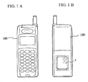
- Fig. 1A is a front view of a mobile terminal employing a non-contact IC system according to a first embodiment of the invention, and Fig. 1B shows its rear view.
- a communication terminal such as a mobile telephone in which a non-contact IC module is mounted.
- numeral 100 designates a mobile telephone (mobile terminal), and numeral 1 designates the non-contact IC system housed in the mobile telephone 100.
- non-contact IC cards do not have an external power source such as a secondary cell or a battery but utilize electric power by electromagnetic induction via the antenna coil as drive power to the IC module.
- the non-contact IC system of the invention utilizes electric power supplied from the battery of the mobile telephone 100 as drive power, and the electric power by electromagnetic induction is primarily utilized for making a decision in controlling the power supply to the IC module.
- Fig. 2 is a block diagram showing the structure of the non-contact IC system 1.
- numeral 1 designates the non-contact IC system
- numeral 2 designates an IC card reader/writer.
- the non-contact IC system 1 is comprised of an antenna coil 11, an IC module 12 for receiving electric power and communication information via radio waves received by the antenna coil 11, a central arithmetic processing unit 13 (a control means and a communication state detection means) for controlling the entire system and the drive power supply to the IC module 12, a regulator 14 connected to a battery 16 for supplying a predetermined drive power to the IC module 12, a voltage detection circuit 15 (power detection means) for detecting the electric power supplied via the antenna coil 11, the battery 16 comprised of secondary cells or the like, a bus 17, and a switch 18.
- the IC module 12 is comprised of a control circuit 21, a power supply circuit 22, and a communication circuit 23.
- the central arithmetic processing unit 13 is comprised of a microcomputer including a CPU and a ROM, RAM, EEPROM (electrically erasable programmable ROM), or the like for storing a program executed by the CPU, or data. It controls the drive power supply to the IC module 12 in accordance with the results of detection of the electric power supplied via the antenna coil 11 and with the communication state of the IC module 12.
- the central arithmetic processing unit 13 may be constructed as a dedicated central arithmetic processing unit for the system for performing various controls in the non-contact IC system 1.
- a control unit may be comprised of the CPU and the like in the mobile telephone and may double as such a unit of the non-contact IC system to run a drive power supply control program.
- an electronic circuit may be used in which a sequential control is performed using a timer, without using the processor or the like.
- the switch 18 is comprised of a physical switch, such as a push button, and/or a software switch using the menu or options configuration on the mobile telephone 100.
- the IC module 12 In the non-contact IC system 1, the IC module 12, the central arithmetic processing unit 13, the regulator 14, the voltage detection circuit 15, and the switch 18 are connected via the bus 17.
- the antenna coil 11 and the IC module 12 form an interface (I/F) from which the central arithmetic processing unit 13 receives information for performing various controls and a drive power supply control, which will be described later.
- I/F interface
- the following describes the operation of the non-contact IC system structured as described above. First, an electric power detecting operation performed between the non-contact IC system 1 and the IC card reader/writer 2 is described.
- the voltage detection circuit 15 constitutes a detection means for detecting the electric power produced by electromagnetic induction.
- the radio wave emitted by the IC card reader/writer 2 arrives at the IC module 12 via the antenna coil 11.
- the IC module 12 performs communication with the IC card reader/writer 2 via the antenna coil 11.
- a communication start or end signal detected by the IC module 12 is conveyed to the central arithmetic processing unit 13 via the bus 17. In this way, the communication state of the IC module 12 is detected
- the central arithmetic processing unit 13 controls the regulator 14 via the bus 17 in accordance with the detection results and turns on or off the drive power supply to the IC module 12.
- the central arithmetic processing unit 13 constitutes a means for controlling the drive power supply to the IC module 12.
- Fig. 3 is a control sequence diagram showing the power supply controlling operation in the non-contact IC system 1.
- the antenna coil 11 detects a weak electric power carrier wave
- electromagnetic induction soon occurs in the antenna coil 11.
- the alternating current produced by the electromagnetic induction is rectified in the power supply circuit 22 in the IC module 12 and outputted to the voltage detection circuit 15 as an electromagnetically induced voltage.
- the voltage detection circuit 15 detects a voltage change and gives a notification to the central arithmetic processing unit 13.
- the central arithmetic processing unit 13 then starts the timer in preparation for the provision of electric power to the IC module 12 (step 201). Thereafter, the central arithmetic processing unit 13 controls the regulator 14 so as to start the provision of electric power to the IC module 12 (step 202).
- the IC module 12 starts communication with the IC card reader/writer 2 after receiving electric power, and notifies the central arithmetic processing unit 13 of the start of communication.
- the central arithmetic processing unit 13 resets the set time in the timer upon receiving notification about the communication start (step 203).
- the IC module 12 Upon completion of communication with the IC card reader/writer 2, the IC module 12 notifies the central arithmetic processing unit 13 of the end of communication.
- the central arithmetic processing unit 13 then resets the set time in the timer upon receiving notification of the end of communication (step 204).
- the central arithmetic processing unit 13 stops the timer (step 205). In response to the time-out, the central arithmetic processing unit 13 controls the regulator 14 so as to terminate the power supply to the IC module 12 (step 206).
- the timer is used for processing the termination of power supply, the detection of error in electric power carrier wave, the detection of communication abnormalities, and the resumption of communication immediately after the termination of communication.
- the timer may be set such that power supply is automatically terminated either in a certain time or immediately after electric power ceases to be detected.
- step 205 is carried out assuming an error detection in the electric power carrier wave, whereby the power supply to the IC module 12 is terminated. Also, following step 203, if there is no notification of the end of communication from the IC module 12 after a predetermined time, step 205 is carried out assuming a communication abnormality, whereby power supply to the IC module 12 is terminated.
- step 204 in consideration of the possibility of the resumption of communication, the communication state is monitored for a predetermined time. The detection of voltage change is ignored for a predetermined time so that the voltage detection circuit 15 will not detect a voltage change immediately after the termination of power supply to the IC module 12 at step 206.
- the set times in the timer that are set at step 201, 203, and 204 are each suitably set.
- the non-contact IC system 1 of the invention is mounted within the casing of the mobile telephone 100 and is comprised of the antenna coil 11, the IC module 12 for receiving electric power and communication information via electric waves received by the antenna coil 11, the central arithmetic processing unit 13 for controlling the entire system and the drive power supply to the IC module 12, the regulator 14 for supplying the drive power to the IC module 12, the voltage detection circuit 15 for detecting the electric power via the antenna coil 11, the battery 16, the bus 17, and the switch 18.
- the central arithmetic processing unit 13 controls the drive power supply to the IC module 12 in accordance with the result of detection of the electric power supplied via the antenna coil 11 and the communication state of the IC module 12, stable communication can be achieved even when the power supply by electromagnetic induction via radio waves is weak or unstable.
- Fig. 4 shows a control sequence diagram of a power supply control operation in the non-contact IC system according to a second embodiment of the invention.
- the steps that are carried out for the same control sequence as in Fig. 3 are indicated with the same reference numbers, and the explanations of the overlapping portions are omitted.
- the hardware structure of the non-contact IC system of the embodiment is the same as that shown in Fig. 2 .
- the detection of voltage change in the voltage detection circuit 15 was described as a trigger for carrying out step 201.
- a change in the state of the switch 18 is detected as such a trigger.
- the central arithmetic processing unit 13 monitors a change in the switch 18. Upon detection of a change, the central arithmetic processing unit 13 starts the timer in preparation for the providing of electric power to the IC module 12 at step 201. Thereafter, it controls the regulator 14 and initiates the provision of electric power to the IC module 12 (step 202). The subsequent operations for power supply control are the same as those of the first embodiment.
- the user of the non-contact IC system can anticipate communication with the IC card reader/writer 2, he or she can change the state of the switch 18 before initiating communication. This makes it possible to provide electric power to the IC module prior to radio wave reception. Hence, communication can be initiated immediately after radio wave reception, whereby communication time can be shortened.
- non-contact IC system is built inside the casing of the mobile telephone 100
- the invention may be applied to any type of mobile terminals as long as it involves a non-contact IC system.
- electronic devices that can function as the terminal for the non-contact IC system 10 include, in addition to the mobile communication terminals such as mobile telephones and PHS (personal handy-phone systems), mobile information terminals such as laptop personal computers and PDAs (personal digital assistants).
- the system may be incorporated in the terminal device or the like as a non-contact IC system function.
- it may be constructed as a non-contact IC card such that the battery and/or the function for controlling the drive power supply to the IC module depend on the terminal device.
- the battery of the terminal device would be shared with the IC module, and the control unit of the terminal device would perform the IC module drive power control function.
- the non-contact IC system is mounted on the mobile terminal device, the battery, the central arithmetic processing unit, or the like can be shared with the mobile terminal device. As a result, the invention can be implemented easily without increasing the number of components and at low cost.
- non-contact IC system While the embodiments referred to the term “non-contact IC system,” this is for explanatory purposes only, and other terms, such as “power supply device,” or “power supply control device,” may be employed. Further, the non-contact IC system may be in the form of a non-contact IC card, such as the EO-card from East Japan Railway Company, for example.
- the type or number of the IC module, voltage detection circuit, regulator, and the like, of which the non-contact IC system is comprised, as well as the manner of setting or resetting the timer, are not limited to those described in the above embodiments.
- power supply can be limited to the communication period, so that battery power consumption can be minimized. Also, stable communication can be achieved even when the power supply by electromagnetic induction via radio waves is weak or unstable.
Landscapes
- Engineering & Computer Science (AREA)
- Physics & Mathematics (AREA)
- Microelectronics & Electronic Packaging (AREA)
- Computer Hardware Design (AREA)
- Theoretical Computer Science (AREA)
- General Physics & Mathematics (AREA)
- Computer Networks & Wireless Communication (AREA)
- Electromagnetism (AREA)
- Power Engineering (AREA)
- General Engineering & Computer Science (AREA)
- Near-Field Transmission Systems (AREA)
- Telephone Function (AREA)
- Mobile Radio Communication Systems (AREA)
Abstract
Description
- The present invention relates to a non-contact IC system and a mobile terminal for transmitting and receiving data using electromagnetic waves as a medium. In particular, it relates to a non-contact IC system in which a non-coritact IC module is mounted in a terminal such as a mobile telephone.
- Recently, IC cards containing IC modules are becoming rapidly common because they can achieve much higher security than magnetic cards. Particularly, a non-contact IC card that makes use of data transmission by electromagnetic induction or the like via radio waves has the advantage of being able to operate with high reliability in a very dusty environment because its IC module is not exposed to the outside.
- The non-contact IC card operates by utilizing radio waves emitted by an IC card reader/writer as electric power via electromagnetic induction in an antenna coil. The non-contact IC card is not always provided with stable electric power because electric power is supplied via radio waves as a medium. In order to assure a stable power supply, non-contact IC cards or non-contact IC systems equipped with an external power source such as a secondary cell, a capacitor, or a battery have been suggested.
- With regard to the provision of power supply to a non-contact IC card,
JP Patent Publication (Kokai) No. 2000-90220 A JP Patent Publication (Kokai) No. 2003-36427 A - In
DE 195 31 625 A1 , a non-contact IC card is disclosed, the card comprising an antenna circuit adapted to transmit and receive an electromagnetic wave as a medium for data transmission, and adapted to receive an electric power transmitted by the electromagnetic wave. Further, the card comprises a data processing and storing unit connected to the antenna circuit and a first and second power source for supplying electric power, the first power source being connected to the data processing and storing unit, the second power source being connected to the antenna circuit and the data processing and storing unit such that the electric power received from the antenna circuit is rectified and saved for supplying power to the data processing and storing unit. Further, a power source switching unit connected to the first and second power source and to the data processing and storing unit is included for switching the electric power supplied to the data processing and the storing unit between the first and the second power source. - The independent claims are delimited against this prior art document.
- However, such conventional non-contact IC cards are problematic in the following respects.
- In order to stably operate a non-contact IC system equipped with a charging system which charges a secondary cell or a capacitor, in a weak or unstable radio wave environment, the secondary cell or the capacitor needs to have been charged. Although it is possible to stably operate the system at all times with a constant supply of electric power from an external power source such as a battery, this would result in an increase in power consumption of such battery. In .. the proposed semiconductor integrated circuit that can seamlessly switch between electric power supplied via the antenna coil and electric power supplied from an external power supply such as a battery, no specific method for realizing power supply control of the non-contact IC system in a mobile terminal such as a mobile telephone has been disclosed.
- The present invention has been made in consideration of such problems, and it is an object of the present invention to provide a non-contact IC system and a mobile terminal capable of performing stable communication even when the power supply by electromagnetic induction via radio waves is weak or unstable.
- The invention is defined by the independent claims.
- Preferred embodiments are set out in the dependent claims.
-
-
Fig. 1A shows a front view of a mobile terminal to which a non-contact IC system according to a first embodiment of the invention is applied.Fig. 1B shows a rear view of a mobile terminal employing the non-contact IC system. -
Fig. 2 is a block diagram showing the structure of the non-contact IC system. -
Fig. 3 is a control sequence diagram showing a power supply control operation of the non-contact IC system -
Fig. 4 is a control sequence diagram showing a power supply control operation of a non-contact IC system according to a second embodiment of the invention. - The invention will be described in greater detail with reference to the attached drawings.
-
Fig. 1A is a front view of a mobile terminal employing a non-contact IC system according to a first embodiment of the invention, andFig. 1B shows its rear view. This is an example in which the invention is applied to a communication terminal such as a mobile telephone in which a non-contact IC module is mounted. - In
Figs. 1A and 1B ,numeral 100 designates a mobile telephone (mobile terminal), andnumeral 1 designates the non-contact IC system housed in themobile telephone 100. - Conventional non-contact IC cards do not have an external power source such as a secondary cell or a battery but utilize electric power by electromagnetic induction via the antenna coil as drive power to the IC module. In contrast, the non-contact IC system of the invention utilizes electric power supplied from the battery of the
mobile telephone 100 as drive power, and the electric power by electromagnetic induction is primarily utilized for making a decision in controlling the power supply to the IC module. -
Fig. 2 is a block diagram showing the structure of thenon-contact IC system 1. - In
Fig. 2 ,numeral 1 designates the non-contact IC system, andnumeral 2 designates an IC card reader/writer. - The
non-contact IC system 1 is comprised of anantenna coil 11, anIC module 12 for receiving electric power and communication information via radio waves received by theantenna coil 11, a central arithmetic processing unit 13 (a control means and a communication state detection means) for controlling the entire system and the drive power supply to theIC module 12, aregulator 14 connected to a battery 16 for supplying a predetermined drive power to theIC module 12, a voltage detection circuit 15 (power detection means) for detecting the electric power supplied via theantenna coil 11, the battery 16 comprised of secondary cells or the like, a bus 17, and aswitch 18. TheIC module 12 is comprised of acontrol circuit 21, apower supply circuit 22, and acommunication circuit 23. - The central
arithmetic processing unit 13 is comprised of a microcomputer including a CPU and a ROM, RAM, EEPROM (electrically erasable programmable ROM), or the like for storing a program executed by the CPU, or data. It controls the drive power supply to theIC module 12 in accordance with the results of detection of the electric power supplied via theantenna coil 11 and with the communication state of theIC module 12. The centralarithmetic processing unit 13 may be constructed as a dedicated central arithmetic processing unit for the system for performing various controls in thenon-contact IC system 1. Alternatively, a control unit may be comprised of the CPU and the like in the mobile telephone and may double as such a unit of the non-contact IC system to run a drive power supply control program. Further alternatively, an electronic circuit may be used in which a sequential control is performed using a timer, without using the processor or the like. - The
switch 18 is comprised of a physical switch, such as a push button, and/or a software switch using the menu or options configuration on themobile telephone 100. - In the
non-contact IC system 1, theIC module 12, the centralarithmetic processing unit 13, theregulator 14, thevoltage detection circuit 15, and theswitch 18 are connected via the bus 17. - The
antenna coil 11 and theIC module 12 form an interface (I/F) from which the centralarithmetic processing unit 13 receives information for performing various controls and a drive power supply control, which will be described later. - The following describes the operation of the non-contact IC system structured as described above. First, an electric power detecting operation performed between the
non-contact IC system 1 and the IC card reader/writer 2 is described. - As a radio wave emitted by the IC card reader/
writer 2 arrives at theIC module 12 via theantenna coil 11, an electromagnetically induced voltage in theIC module 12 increases due to electromagnetic induction in theantenna coil 11. A voltage change due to the increase in the electromagnetically induced voltage is detected by thevoltage detection circuit 15 and then conveyed to the centralarithmetic processing unit 13 via the bus 17. Thevoltage detection circuit 15 constitutes a detection means for detecting the electric power produced by electromagnetic induction. - Also, the radio wave emitted by the IC card reader/
writer 2 arrives at theIC module 12 via theantenna coil 11. When this wave contains a communication wave, theIC module 12 performs communication with the IC card reader/writer 2 via theantenna coil 11. A communication start or end signal detected by theIC module 12 is conveyed to the centralarithmetic processing unit 13 via the bus 17. In this way, the communication state of theIC module 12 is detected - The central
arithmetic processing unit 13 controls theregulator 14 via the bus 17 in accordance with the detection results and turns on or off the drive power supply to theIC module 12. The centralarithmetic processing unit 13 constitutes a means for controlling the drive power supply to theIC module 12. -
Fig. 3 is a control sequence diagram showing the power supply controlling operation in thenon-contact IC system 1. - As the
antenna coil 11 detects a weak electric power carrier wave, electromagnetic induction soon occurs in theantenna coil 11. The alternating current produced by the electromagnetic induction is rectified in thepower supply circuit 22 in theIC module 12 and outputted to thevoltage detection circuit 15 as an electromagnetically induced voltage. Thevoltage detection circuit 15 detects a voltage change and gives a notification to the centralarithmetic processing unit 13. The centralarithmetic processing unit 13 then starts the timer in preparation for the provision of electric power to the IC module 12 (step 201). Thereafter, the centralarithmetic processing unit 13 controls theregulator 14 so as to start the provision of electric power to the IC module 12 (step 202). - The
IC module 12 starts communication with the IC card reader/writer 2 after receiving electric power, and notifies the centralarithmetic processing unit 13 of the start of communication. The centralarithmetic processing unit 13 resets the set time in the timer upon receiving notification about the communication start (step 203). Upon completion of communication with the IC card reader/writer 2, theIC module 12 notifies the centralarithmetic processing unit 13 of the end of communication. The centralarithmetic processing unit 13 then resets the set time in the timer upon receiving notification of the end of communication (step 204). - When the timer runs out, the central
arithmetic processing unit 13 stops the timer (step 205). In response to the time-out, the centralarithmetic processing unit 13 controls theregulator 14 so as to terminate the power supply to the IC module 12 (step 206). The timer is used for processing the termination of power supply, the detection of error in electric power carrier wave, the detection of communication abnormalities, and the resumption of communication immediately after the termination of communication. The timer may be set such that power supply is automatically terminated either in a certain time or immediately after electric power ceases to be detected. - Following
step 201, if there is no notification of communication start from theIC module 12 after a predetermined time,step 205 is carried out assuming an error detection in the electric power carrier wave, whereby the power supply to theIC module 12 is terminated. Also, followingstep 203, if there is no notification of the end of communication from theIC module 12 after a predetermined time,step 205 is carried out assuming a communication abnormality, whereby power supply to theIC module 12 is terminated. - After
step 204, in consideration of the possibility of the resumption of communication, the communication state is monitored for a predetermined time. The detection of voltage change is ignored for a predetermined time so that thevoltage detection circuit 15 will not detect a voltage change immediately after the termination of power supply to theIC module 12 atstep 206. The set times in the timer that are set atstep - As described above, the
non-contact IC system 1 of the invention is mounted within the casing of themobile telephone 100 and is comprised of theantenna coil 11, theIC module 12 for receiving electric power and communication information via electric waves received by theantenna coil 11, the centralarithmetic processing unit 13 for controlling the entire system and the drive power supply to theIC module 12, theregulator 14 for supplying the drive power to theIC module 12, thevoltage detection circuit 15 for detecting the electric power via theantenna coil 11, the battery 16, the bus 17, and theswitch 18. Because the centralarithmetic processing unit 13 controls the drive power supply to theIC module 12 in accordance with the result of detection of the electric power supplied via theantenna coil 11 and the communication state of theIC module 12, stable communication can be achieved even when the power supply by electromagnetic induction via radio waves is weak or unstable. - In conventional non-contact IC systems in which electric power is constantly supplied to the IC module, battery power is consumed even when no communication is being performed. However, in accordance with the non-contact IC system of the invention, because the central
arithmetic processing unit 13 monitors the electric power by electromagnetic induction in theantenna coil 11 and the communication of theIC module 12, the power supply to theIC module 12 can be limited to the communication period. Therefore, battery power consumption can be minimized. - In addition, even when the power supply by radio waves is weak or unstable due to the distance from the IC card reader/
writer 2, for example, stable communication can be achieved because stable supply of power from the battery 16 is enabled. Also, as compared with conventional non-contact IC cards, the communication distance from the IC card reader/writer 2 can be increased. -
Fig. 4 shows a control sequence diagram of a power supply control operation in the non-contact IC system according to a second embodiment of the invention. The steps that are carried out for the same control sequence as inFig. 3 are indicated with the same reference numbers, and the explanations of the overlapping portions are omitted. The hardware structure of the non-contact IC system of the embodiment is the same as that shown inFig. 2 . - In the first embodiment, the detection of voltage change in the
voltage detection circuit 15 was described as a trigger for carrying outstep 201. Instead, in the second embodiment, as shown inFig. 4 , a change in the state of theswitch 18 is detected as such a trigger. - Namely, the central
arithmetic processing unit 13 monitors a change in theswitch 18. Upon detection of a change, the centralarithmetic processing unit 13 starts the timer in preparation for the providing of electric power to theIC module 12 atstep 201. Thereafter, it controls theregulator 14 and initiates the provision of electric power to the IC module 12 (step 202). The subsequent operations for power supply control are the same as those of the first embodiment. - In accordance with the second embodiment, because the user of the non-contact IC system can anticipate communication with the IC card reader/
writer 2, he or she can change the state of theswitch 18 before initiating communication. This makes it possible to provide electric power to the IC module prior to radio wave reception. Hence, communication can be initiated immediately after radio wave reception, whereby communication time can be shortened. - While the above-described embodiments show examples where the non-contact IC system is built inside the casing of the
mobile telephone 100, the invention may be applied to any type of mobile terminals as long as it involves a non-contact IC system. Examples of electronic devices that can function as the terminal for the non-contact IC system 10 include, in addition to the mobile communication terminals such as mobile telephones and PHS (personal handy-phone systems), mobile information terminals such as laptop personal computers and PDAs (personal digital assistants). - While the embodiments showed examples where the
non-contact IC system 1 is mounted within the casing of the terminal, the system may be incorporated in the terminal device or the like as a non-contact IC system function. Alternatively, it may be constructed as a non-contact IC card such that the battery and/or the function for controlling the drive power supply to the IC module depend on the terminal device. In this case, the battery of the terminal device would be shared with the IC module, and the control unit of the terminal device would perform the IC module drive power control function. In any event, because the non-contact IC system is mounted on the mobile terminal device, the battery, the central arithmetic processing unit, or the like can be shared with the mobile terminal device. As a result, the invention can be implemented easily without increasing the number of components and at low cost. - While the embodiments referred to the term "non-contact IC system," this is for explanatory purposes only, and other terms, such as "power supply device," or "power supply control device," may be employed. Further, the non-contact IC system may be in the form of a non-contact IC card, such as the EO-card from East Japan Railway Company, for example.
- Furthermore, the type or number of the IC module, voltage detection circuit, regulator, and the like, of which the non-contact IC system is comprised, as well as the manner of setting or resetting the timer, are not limited to those described in the above embodiments.
- As specifically described above, in accordance with the invention, power supply can be limited to the communication period, so that battery power consumption can be minimized. Also, stable communication can be achieved even when the power supply by electromagnetic induction via radio waves is weak or unstable.
Claims (7)
- An electric circuit connecting an antenna coil (11) and a battery (16), said electric circuit comprising:a carrier wave detection means (15) adapted to detect a carrier wave supplied via said antenna coil (11),a communication means (23) adapted to communicate via said antenna coil (11),a power control means (13) adapted to control a drive power supply from the battery (16) to the communication means (23),characterized in thatthe power control means (13) is adapted to terminate the drive power supply from the battery to the communication means (23) either in a certain time after said carrier wave ceases to be detected by said carrier wave detection means (15) or immediately after said carrier wave ceases to be detected by said carrier wave detection means (15).
- A terminal device (100) comprising the electric circuit of claim 1, further comprising the antenna coil (11) and the battery (16).
- The terminal device (100) according to claim 2, wherein the power control means controls that the power from the battery to the communication means is supplied from the start of the detection of the carrier wave to the end of the detection of the carrier wave detected by the carrier wave detection means (15).
- The terminal device (100) according to claim 2, wherein the detection of the carrier wave by the carrier wave detection means (15) is a detection of a voltage produced by the electromagnetic wave recevied by the antenna coil.
- The terminal device (100) according to claim 4, wherein the voltage is an electromagnetically induced voltage.
- The terminal device (100) according to claim 2, wherein the detection of the carrier wave by the carrier wave detection means (15) is a detection of a power produced by the electromagnetic wave received by the antenna coil (11).
- A method of controlling power supply, comprising:communicating with an IC card reader/writer (2) using a communication means (23), with supplying electric power from a battery (16) to the communication means (23);characterized bydetecting a ceasing of the carrier wave for the communication from the IC card reader/writer (2); andterminating the supply of the electric power from the battery (16) to the communication means (23) either in a certain time after the carrier wave ceases to be detected or immediately after the carrier wave ceases to be detected.
Applications Claiming Priority (2)
| Application Number | Priority Date | Filing Date | Title |
|---|---|---|---|
| JP2003315323 | 2003-09-08 | ||
| PCT/JP2004/012929 WO2005027034A1 (en) | 2003-09-08 | 2004-09-06 | Non-contact ic system and mobile terminal |
Publications (3)
| Publication Number | Publication Date |
|---|---|
| EP1667056A1 EP1667056A1 (en) | 2006-06-07 |
| EP1667056A4 EP1667056A4 (en) | 2008-08-20 |
| EP1667056B1 true EP1667056B1 (en) | 2012-02-01 |
Family
ID=34308424
Family Applications (1)
| Application Number | Title | Priority Date | Filing Date |
|---|---|---|---|
| EP04787633A Revoked EP1667056B1 (en) | 2003-09-08 | 2004-09-06 | Non-contact ic system and mobile terminal |
Country Status (6)
| Country | Link |
|---|---|
| US (1) | US20070057073A1 (en) |
| EP (1) | EP1667056B1 (en) |
| JP (1) | JPWO2005027034A1 (en) |
| KR (2) | KR100965323B1 (en) |
| CN (2) | CN1879116B (en) |
| WO (1) | WO2005027034A1 (en) |
Families Citing this family (17)
| Publication number | Priority date | Publication date | Assignee | Title |
|---|---|---|---|---|
| US7764046B2 (en) * | 2006-08-31 | 2010-07-27 | Semiconductor Energy Laboratory Co., Ltd. | Power storage device and semiconductor device provided with the power storage device |
| JP2008092304A (en) * | 2006-10-02 | 2008-04-17 | Matsushita Electric Ind Co Ltd | Mobile terminal device |
| JP2008161045A (en) | 2006-11-28 | 2008-07-10 | Semiconductor Energy Lab Co Ltd | Semiconductor device, method for charging semiconductor device, and communication system using the semiconductor device |
| EP1936541B1 (en) * | 2006-12-22 | 2017-08-30 | EM Microelectronic-Marin SA | On/off battery charger with power supply protection for monolithic integrated circuits using the energy from the antenna |
| JP4671001B2 (en) | 2008-07-04 | 2011-04-13 | 株式会社村田製作所 | Wireless IC device |
| CN101668350B (en) * | 2008-09-01 | 2012-07-25 | 联想(北京)有限公司 | Mobile-terminal state-switching method and mobile terminal |
| CN101754458B (en) * | 2008-12-01 | 2016-10-05 | 联想(北京)有限公司 | The Working mode switching method of communication system and mobile terminal |
| FR2944632B1 (en) * | 2009-04-17 | 2011-05-06 | Oberthur Technologies | ELECTRONIC DEVICE COMPRISING A MICROCIRCUIT CARD AND AN AUXILIARY BATTERY. |
| EP2369752A1 (en) * | 2010-03-22 | 2011-09-28 | Gemalto SA | Portable device with self-contained battery and radiofrequency communication interface |
| JP5821216B2 (en) * | 2011-03-01 | 2015-11-24 | ソニー株式会社 | Information processing apparatus, power control method for information processing apparatus, and program |
| JP6045141B2 (en) | 2011-12-05 | 2016-12-14 | キヤノン株式会社 | Electronic device and program |
| JP5939780B2 (en) | 2011-12-08 | 2016-06-22 | キヤノン株式会社 | Electronics |
| CN103580294A (en) * | 2012-07-27 | 2014-02-12 | 十速兴业科技(深圳)有限公司 | Module for converting radio waves into electric energy and low-power electronic device and method utilizing the module |
| CN103633829A (en) * | 2012-08-24 | 2014-03-12 | 十速兴业科技(深圳)有限公司 | Electromagnetic interference signal eliminating module, system thereof and method thereof |
| US9595823B2 (en) * | 2014-01-24 | 2017-03-14 | Intel Corporation | Low power circuit for transistor electrical overstress protection in high voltage applications |
| KR102332621B1 (en) * | 2014-11-21 | 2021-12-01 | 삼성전자주식회사 | Signal Receiving and Transmitting circuit and electronic device including the same |
| CN108124473A (en) * | 2017-12-11 | 2018-06-05 | 深圳前海达闼云端智能科技有限公司 | Writer hanging method and terminal |
Family Cites Families (15)
| Publication number | Priority date | Publication date | Assignee | Title |
|---|---|---|---|---|
| KR100227055B1 (en) * | 1990-11-06 | 1999-10-15 | 로데릭 더블류 루이스 | Dual mode electronic identification system and tag |
| DE69228473T3 (en) * | 1991-12-04 | 2002-07-11 | Citizen Watch Co., Ltd. | MEDIA |
| JPH0830749A (en) * | 1994-07-13 | 1996-02-02 | Mitsubishi Electric Corp | Non-contact IC card |
| JPH0869513A (en) | 1994-08-30 | 1996-03-12 | Mitsubishi Denki Semiconductor Software Kk | Non-contact IC card |
| WO1996036099A2 (en) * | 1995-05-11 | 1996-11-14 | Ericsson Inc. | Power control circuit for a battery operated device |
| US5943624A (en) * | 1996-07-15 | 1999-08-24 | Motorola, Inc. | Contactless smartcard for use in cellular telephone |
| SG54559A1 (en) * | 1996-09-13 | 1998-11-16 | Hitachi Ltd | Power transmission system ic card and information communication system using ic card |
| JPH10261053A (en) * | 1997-03-18 | 1998-09-29 | Toshiba Corp | Wireless card adapter |
| US6489883B1 (en) * | 1997-04-30 | 2002-12-03 | Matsushita Electric Industrial Co., Ltd. | Non-contact data carrier system |
| GB2358991B (en) * | 1999-09-14 | 2002-02-13 | Motorola Inc | Wireless radio frequency peripheral interface for a cellular communication device |
| JP2002057617A (en) * | 2000-08-09 | 2002-02-22 | Toshiba Tec Corp | Wireless terminal device, wireless communication system, and wireless terminal device initial setting method |
| CN1292382C (en) * | 2001-03-02 | 2006-12-27 | 索尼公司 | Read/write chips with power management |
| JP2003036427A (en) * | 2001-03-02 | 2003-02-07 | Sony Corp | Semiconductor integrated circuit device, portable terminal device, and settlement method |
| US6944424B2 (en) * | 2001-07-23 | 2005-09-13 | Intermec Ip Corp. | RFID tag having combined battery and passive power source |
| JP4558259B2 (en) * | 2002-05-23 | 2010-10-06 | シャープ株式会社 | Combination IC card |
-
2004
- 2004-09-06 WO PCT/JP2004/012929 patent/WO2005027034A1/en not_active Ceased
- 2004-09-06 JP JP2005513860A patent/JPWO2005027034A1/en active Pending
- 2004-09-06 EP EP04787633A patent/EP1667056B1/en not_active Revoked
- 2004-09-06 US US10/570,875 patent/US20070057073A1/en not_active Abandoned
- 2004-09-06 KR KR1020087029449A patent/KR100965323B1/en not_active Expired - Fee Related
- 2004-09-06 CN CN2004800327696A patent/CN1879116B/en not_active Expired - Fee Related
- 2004-09-06 CN CN2011101061210A patent/CN102222250A/en active Pending
- 2004-09-06 KR KR1020067004661A patent/KR100939870B1/en not_active Expired - Fee Related
Also Published As
| Publication number | Publication date |
|---|---|
| EP1667056A1 (en) | 2006-06-07 |
| KR20060060035A (en) | 2006-06-02 |
| EP1667056A4 (en) | 2008-08-20 |
| KR100939870B1 (en) | 2010-01-29 |
| US20070057073A1 (en) | 2007-03-15 |
| CN102222250A (en) | 2011-10-19 |
| KR20080109944A (en) | 2008-12-17 |
| CN1879116A (en) | 2006-12-13 |
| CN1879116B (en) | 2011-06-08 |
| KR100965323B1 (en) | 2010-06-22 |
| JPWO2005027034A1 (en) | 2007-11-08 |
| WO2005027034A1 (en) | 2005-03-24 |
Similar Documents
| Publication | Publication Date | Title |
|---|---|---|
| EP1667056A1 (en) | Non-contact ic system and mobile terminal | |
| EP3293856B1 (en) | Wireless power charging system | |
| US7344074B2 (en) | Mobile terminal featuring smart card interrupt | |
| KR100560768B1 (en) | Dual Interface Integrated Circuit Card | |
| CN113497641B (en) | Communication device and operation method | |
| EP2518587B1 (en) | Management of secure element deadlock | |
| EP1280099A4 (en) | CHIP FOR CONTACTLESS READER / WRITER HAVING A FUNCTION FOR MANAGING THE POWER SUPPLY | |
| US7789313B2 (en) | Fully simultaneous information on variations in status for an object with a dual interface | |
| CN101626257A (en) | Communication apparatus | |
| CN111641437B (en) | Near Field Communication and Wireless Charging Antenna Module and Electronic Device | |
| US12253894B2 (en) | Electronic device powering | |
| EP2163968A2 (en) | IC chip, information processing device, information processing system, and programs | |
| US20080048042A1 (en) | Immunity to Variations in Limited Resources, Provided to an Object with a Dual Interface | |
| US12282374B2 (en) | Electronic card | |
| JP2009094883A (en) | Auxiliary power system for cellular phone | |
| US8811972B2 (en) | Communication terminal and communication control method | |
| JPH11313024A (en) | Radio card for personal computer | |
| US7359695B2 (en) | Circuit for a data carrier, which circuit can be switched from an energy-saving processing mode to a normal-consumption processing mode | |
| US12346757B2 (en) | Electronic device powering | |
| WO2008059564A1 (en) | Reader/writer device for noncontact ic card, communication system and noncontact communication method | |
| CN115529057B (en) | Electronic device power supply | |
| CN115706962A (en) | Electronic device power supply | |
| HK1140288A (en) | Ic chip, information processing device, information processing system, and programs |
Legal Events
| Date | Code | Title | Description |
|---|---|---|---|
| PUAI | Public reference made under article 153(3) epc to a published international application that has entered the european phase |
Free format text: ORIGINAL CODE: 0009012 |
|
| 17P | Request for examination filed |
Effective date: 20060308 |
|
| AK | Designated contracting states |
Kind code of ref document: A1 Designated state(s): DE FR GB |
|
| DAX | Request for extension of the european patent (deleted) | ||
| RBV | Designated contracting states (corrected) |
Designated state(s): DE FR GB |
|
| A4 | Supplementary search report drawn up and despatched |
Effective date: 20080718 |
|
| RIC1 | Information provided on ipc code assigned before grant |
Ipc: H01Q 1/22 20060101ALI20080714BHEP Ipc: G06F 1/26 20060101ALI20080714BHEP Ipc: G06K 19/07 20060101AFI20050331BHEP Ipc: H02J 17/00 20060101ALI20080714BHEP Ipc: H04M 1/02 20060101ALI20080714BHEP Ipc: G06K 7/00 20060101ALI20080714BHEP |
|
| 17Q | First examination report despatched |
Effective date: 20090105 |
|
| GRAP | Despatch of communication of intention to grant a patent |
Free format text: ORIGINAL CODE: EPIDOSNIGR1 |
|
| GRAS | Grant fee paid |
Free format text: ORIGINAL CODE: EPIDOSNIGR3 |
|
| GRAA | (expected) grant |
Free format text: ORIGINAL CODE: 0009210 |
|
| AK | Designated contracting states |
Kind code of ref document: B1 Designated state(s): DE FR GB |
|
| REG | Reference to a national code |
Ref country code: GB Ref legal event code: FG4D |
|
| REG | Reference to a national code |
Ref country code: DE Ref legal event code: R096 Ref document number: 602004036384 Country of ref document: DE Effective date: 20120329 |
|
| PLBI | Opposition filed |
Free format text: ORIGINAL CODE: 0009260 |
|
| 26 | Opposition filed |
Opponent name: GIESECKE & DEVRIENT GMBH Effective date: 20121026 |
|
| PLAX | Notice of opposition and request to file observation + time limit sent |
Free format text: ORIGINAL CODE: EPIDOSNOBS2 |
|
| REG | Reference to a national code |
Ref country code: DE Ref legal event code: R026 Ref document number: 602004036384 Country of ref document: DE Effective date: 20121026 |
|
| PLAF | Information modified related to communication of a notice of opposition and request to file observations + time limit |
Free format text: ORIGINAL CODE: EPIDOSCOBS2 |
|
| PLBB | Reply of patent proprietor to notice(s) of opposition received |
Free format text: ORIGINAL CODE: EPIDOSNOBS3 |
|
| PGFP | Annual fee paid to national office [announced via postgrant information from national office to epo] |
Ref country code: DE Payment date: 20140922 Year of fee payment: 11 |
|
| REG | Reference to a national code |
Ref country code: DE Ref legal event code: R231 Ref document number: 602004036384 Country of ref document: DE |
|
| PGFP | Annual fee paid to national office [announced via postgrant information from national office to epo] |
Ref country code: FR Payment date: 20140919 Year of fee payment: 11 Ref country code: GB Payment date: 20140919 Year of fee payment: 11 |
|
| PLAY | Examination report in opposition despatched + time limit |
Free format text: ORIGINAL CODE: EPIDOSNORE2 |
|
| REG | Reference to a national code |
Ref country code: GB Ref legal event code: S29 Free format text: OFFER FILED; APPLICATION FILED 8 DECEMBER 2014 |
|
| PLBC | Reply to examination report in opposition received |
Free format text: ORIGINAL CODE: EPIDOSNORE3 |
|
| PG25 | Lapsed in a contracting state [announced via postgrant information from national office to epo] |
Ref country code: DE Free format text: LAPSE BECAUSE OF THE APPLICANT RENOUNCES Effective date: 20141125 |
|
| REG | Reference to a national code |
Ref country code: GB Ref legal event code: S29 Free format text: OFFER ACCEPTED |
|
| RDAF | Communication despatched that patent is revoked |
Free format text: ORIGINAL CODE: EPIDOSNREV1 |
|
| PG25 | Lapsed in a contracting state [announced via postgrant information from national office to epo] |
Ref country code: GB Free format text: LAPSE BECAUSE OF THE APPLICANT RENOUNCES Effective date: 20150318 |
|
| RDAG | Patent revoked |
Free format text: ORIGINAL CODE: 0009271 |
|
| STAA | Information on the status of an ep patent application or granted ep patent |
Free format text: STATUS: PATENT REVOKED |
|
| 27W | Patent revoked |
Effective date: 20150425 |