EP1662612A1 - A device for reflecting electromagnetic radiation - Google Patents
A device for reflecting electromagnetic radiation Download PDFInfo
- Publication number
- EP1662612A1 EP1662612A1 EP05257072A EP05257072A EP1662612A1 EP 1662612 A1 EP1662612 A1 EP 1662612A1 EP 05257072 A EP05257072 A EP 05257072A EP 05257072 A EP05257072 A EP 05257072A EP 1662612 A1 EP1662612 A1 EP 1662612A1
- Authority
- EP
- European Patent Office
- Prior art keywords
- impedance
- antenna
- state
- ideal
- antennas
- Prior art date
- Legal status (The legal status is an assumption and is not a legal conclusion. Google has not performed a legal analysis and makes no representation as to the accuracy of the status listed.)
- Ceased
Links
Images
Classifications
-
- H—ELECTRICITY
- H05—ELECTRIC TECHNIQUES NOT OTHERWISE PROVIDED FOR
- H05K—PRINTED CIRCUITS; CASINGS OR CONSTRUCTIONAL DETAILS OF ELECTRIC APPARATUS; MANUFACTURE OF ASSEMBLAGES OF ELECTRICAL COMPONENTS
- H05K1/00—Printed circuits
- H05K1/16—Printed circuits incorporating printed electric components, e.g. printed resistors, capacitors or inductors
-
- H—ELECTRICITY
- H01—ELECTRIC ELEMENTS
- H01Q—ANTENNAS, i.e. RADIO AERIALS
- H01Q15/00—Devices for reflection, refraction, diffraction or polarisation of waves radiated from an antenna, e.g. quasi-optical devices
- H01Q15/14—Reflecting surfaces; Equivalent structures
- H01Q15/148—Reflecting surfaces; Equivalent structures with means for varying the reflecting properties
-
- H—ELECTRICITY
- H01—ELECTRIC ELEMENTS
- H01Q—ANTENNAS, i.e. RADIO AERIALS
- H01Q19/00—Combinations of primary active antenna elements and units with secondary devices, e.g. with quasi-optical devices, for giving the antenna a desired directional characteristic
- H01Q19/10—Combinations of primary active antenna elements and units with secondary devices, e.g. with quasi-optical devices, for giving the antenna a desired directional characteristic using reflecting surfaces
-
- H—ELECTRICITY
- H01—ELECTRIC ELEMENTS
- H01Q—ANTENNAS, i.e. RADIO AERIALS
- H01Q21/00—Antenna arrays or systems
- H01Q21/0006—Particular feeding systems
- H01Q21/0018—Space- fed arrays
-
- H—ELECTRICITY
- H01—ELECTRIC ELEMENTS
- H01Q—ANTENNAS, i.e. RADIO AERIALS
- H01Q23/00—Antennas with active circuits or circuit elements integrated within them or attached to them
-
- H—ELECTRICITY
- H01—ELECTRIC ELEMENTS
- H01Q—ANTENNAS, i.e. RADIO AERIALS
- H01Q3/00—Arrangements for changing or varying the orientation or the shape of the directional pattern of the waves radiated from an antenna or antenna system
- H01Q3/44—Arrangements for changing or varying the orientation or the shape of the directional pattern of the waves radiated from an antenna or antenna system varying the electric or magnetic characteristics of reflecting, refracting, or diffracting devices associated with the radiating element
- H01Q3/46—Active lenses or reflecting arrays
-
- H—ELECTRICITY
- H05—ELECTRIC TECHNIQUES NOT OTHERWISE PROVIDED FOR
- H05K—PRINTED CIRCUITS; CASINGS OR CONSTRUCTIONAL DETAILS OF ELECTRIC APPARATUS; MANUFACTURE OF ASSEMBLAGES OF ELECTRICAL COMPONENTS
- H05K1/00—Printed circuits
- H05K1/18—Printed circuits structurally associated with non-printed electric components
- H05K1/181—Printed circuits structurally associated with non-printed electric components associated with surface mounted components
-
- H—ELECTRICITY
- H05—ELECTRIC TECHNIQUES NOT OTHERWISE PROVIDED FOR
- H05K—PRINTED CIRCUITS; CASINGS OR CONSTRUCTIONAL DETAILS OF ELECTRIC APPARATUS; MANUFACTURE OF ASSEMBLAGES OF ELECTRICAL COMPONENTS
- H05K2201/00—Indexing scheme relating to printed circuits covered by H05K1/00
- H05K2201/09—Shape and layout
- H05K2201/09209—Shape and layout details of conductors
- H05K2201/09372—Pads and lands
- H05K2201/0949—Pad close to a hole, not surrounding the hole
-
- H—ELECTRICITY
- H05—ELECTRIC TECHNIQUES NOT OTHERWISE PROVIDED FOR
- H05K—PRINTED CIRCUITS; CASINGS OR CONSTRUCTIONAL DETAILS OF ELECTRIC APPARATUS; MANUFACTURE OF ASSEMBLAGES OF ELECTRICAL COMPONENTS
- H05K2201/00—Indexing scheme relating to printed circuits covered by H05K1/00
- H05K2201/10—Details of components or other objects attached to or integrated in a printed circuit board
- H05K2201/10007—Types of components
- H05K2201/10166—Transistor
-
- H—ELECTRICITY
- H05—ELECTRIC TECHNIQUES NOT OTHERWISE PROVIDED FOR
- H05K—PRINTED CIRCUITS; CASINGS OR CONSTRUCTIONAL DETAILS OF ELECTRIC APPARATUS; MANUFACTURE OF ASSEMBLAGES OF ELECTRICAL COMPONENTS
- H05K3/00—Apparatus or processes for manufacturing printed circuits
- H05K3/40—Forming printed elements for providing electric connections to or between printed circuits
- H05K3/42—Plated through-holes or plated via connections
- H05K3/429—Plated through-holes specially for multilayer circuits, e.g. having connections to inner circuit layers
Definitions
- the present invention relates to a device for reflecting electromagnetic radiation.
- Microwave and millimeter-wave retlectarrays are antenna arrays in which each antenna is connected to a variable impedance device. If the variable impedance device is a resistive device, ideally it is biased at either short-circuit or open-circuit states or at least at states of very low or very high resistance compared to the antenna impedance. In this way, the antenna and variable impedance device combination acts as a variable-phase reflecting element. With appropriate control signals applied to the variable impedance devices, the reflectarray can be used as an adjustable mirror with the capability of focusing, steering, or splitting a beam of electromagnetic radiation.
- Diodes have typically been used as the variable impedance devices in reflectarrays although transistors have also been used. Many low cost transistors are able to provide the desired impedance characteristics at relatively low radio frequency ranges (e.g., less than 10 GHz). However, these low cost transistors do not necessarily provide the desired impedance performance characteristics at relatively high radio frequency ranges (e.g., greater than 20 GHz). More expensively packaged transistors as well as more exotic devices, such as ferroelectric capacitors and ferrite switches, are readily able to provide the desired impedance characteristics at the higher frequency ranges, but the number of transistors, capacitors, or switches required for many reflectarray applications combined with the high cost of each packaged device makes reflectarrays with such devices prohibitively expensive.
- the present invention seeks to provide an improved device for reflecting electromagnetic radiation and an improved reflectarray.
- the preferred embodiments provides a reflectarray that exhibits the desired impedance characteristics and that is economical to implement.
- a reflectarray utilizes switching devices with non-ideal impedance characteristics to vary the impedance of reflecting elements.
- the antennas of the reflecting elements are configured as a function of the impedance of the non-ideal switching devices to provide optimal phase-amplitude performance.
- the antennas are configured such that the impedance of each antenna is proportional to the square root of the impedance of the non-ideal switching devices when in an on state and when in an off state.
- Configuring the antennas as a function of the impedance of the non-ideal switching devices enables a reflectarray to achieve switching between 0 and 180 degree phase-amplitude states while utilizing low-cost switching devices, such as surface mount field effect transistors, which exhibit non-ideal impedance characteristics over the operating frequency range of the reflectarray.
- a reflectarray utilizes switching devices with non-ideal impedance characteristics to vary the impedance of reflecting elements.
- the antennas of the reflecting elements are configured as a function of the impedance of the non-ideal switching devices to provide optimal phase-amplitude performance.
- the antennas are configured such that the impedance of each antenna is proportional to the square root of the impedance of the non-ideal switching devices when in an on states and when in an off state.
- Reflectarrays are passive systems that reflect externally provided electromagnetic radiation.
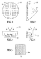
- Fig. 1 depicts an example of a reflectarray 10 for microwave and millimeter-wave applications.
- the reflectarray includes distinct reflecting elements 12 that reflect electromagnetic radiation with varying phase depending on their impedance state. Ideally, the reflecting elements reflect ' electromagnetic radiation with a phase shift of 180 degrees when their impedance is high relative to when their impedance is low.
- the reflecting elements are individually controllable and the reflectarray is typically supported by driver electronics (not shown in Fig. 1).
- the reflectarray is formed on and/or in a substrate 14 such as a printed circuit board. In one example, the reflectarray has a surface area of approximately one meter square and is covered with 10,000 to 100,000 individually controllable reflecting elements.
- Electromagnetic radiation can be provided to the reflectarray from a source such as a horn.
- Fig. 2 depicts a side view of a reflectarray 10 and a horn 16 that is configured to provide electromagnetic radiation to the reflectarray.
- a horn is shown as the source of the electromagnetic radiation in Fig. 2, other sources of electromagnetic radiation are possible.
- Fig. 3 depicts a functional design of one of the individual reflecting elements 12 from Fig. 1.
- the reflecting element includes an antenna 20 and a non-ideal switching device 22.
- the antenna functions to absorb or reflect a beam of electromagnetic radiation to varying degrees depending on the impedance level of the reflecting element.
- the antenna is represented here as a generic dipole antenna for description purposes although other types of antennas are contemplated.
- Example antenna types that can be incorporated into a reflectarray include patch, dipole, monopole, loop, and dielectric resonator type antennas. In reflectarray applications, the antennas are often formed in a single plane on the surface of the reflectarray substrate.
- the antennas have an impedance characteristic that is a function of the antenna design parameters. Design parameters of antennas include but are not limited to, physical attributes such as the dielectric material of construction, the thickness of the dielectric material, shape of the antenna, length and width of the antenna, feed location, and thickness of the antenna metal layer.
- the non-ideal switching device 22 changes the impedance state of the reflecting element 22 by changing its resistive state.
- a low resistive state e.g., a , closed or "short" circuit
- a high resistive state e.g., an open circuit
- Z 0
- the non-ideal switching device does not necessarily provide the maximum phase state performance regardless of the impedance of the corresponding antenna, where maximum phase state performance involves switching between 0 and 180 degree phase states.
- the antennas of a reflectarray that utilizes non-ideal switching devices are specifically designed to provide optimal phase performance, where the optimal phase state performance of a reflecting element is the point at which the reflecting element is closest to switching between 0 and 180 degree phase-amplitude states.
- the antennas are configured as a function of the impedance of the non-ideal switching devices.
- the antennas are designed such that the impedance of the antennas is a function of impedance characteristics of the non-ideal switching devices. Further, the antennas are configured as a function of the impedance of the non-ideal switching devices in the on state, Z on , and the impedance of the non-ideal switching device in the off state, Z off . In a particular embodiment, the phase state performance of a reflecting element is optimized when the antennas are configured such that the impedance of each antenna is conjugate to the square root of the impedance of the non-ideal switching devices when in the on and off impedance states, Z on and Z off .
- the impedance of each antenna is the complex conjugate of the geometric mean of the on and off impedance states, Z on and Z off , of the corresponding non-ideal switching device.
- Z antenna ⁇ Z on Z off
- Z antenna ⁇ Z on Z off
- Designing an antenna that exhibits optimal phase-amplitude performance involves determining the on and off impedances, Z on and Z off of the particular non-ideal switching device that is used in the reflecting elements. Design parameters of the antenna are then manipulated to produce an antenna with an impedance that matches the relationship expressed in equation (1) above.
- An antenna that satisfies equation (1) can be designed as long as Z on and Z off are determined to be distinct values.
- Fig. 4 depicts a functional diagram of a reflecting element 12 in which a three-terminal solid-state transistor is used as the non-ideal switching device 22.
- the three-terminal solid-state transistor is a FET with a source 26, a drain 28, and a gate 30. The source and drain are connected to opposite terminals of the antenna 20 and the drain is connected to some driver electronics (not shown).
- the source is DC-grounded and the drain is either DC-grounded or floating, depending on the application.
- the source-drain radio frequency impedance is nominally high when the gate-source voltage V gs is zero or negative and low when V gs is sufficiently positive.
- the source-drain radio frequency impedance is nominally low when V gs is zero or positive and high when V gs is sufficiently negative.
- the antennas 20 in the reflectarray 10 are planar patch antennas.
- Fig. 5 depicts an example of a top view of a planar patch antenna 20a.
- the planar patch antenna includes a via connector 32 that is electrically connected to the drain of a corresponding solid-state transistor.
- Design criteria of the planar patch antenna that affect the antenna's impedance include, for example, dielectric material of construction, thickness of the dielectric, width of the patch, feed point, and planar metal thickness.
- the planar patch antenna is formed by depositing a metal layer (e.g., gold) on the surface of the reflectarray substrate.
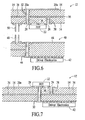
- Fig. 6 depicts a side view of a reflecting element 12 that utilizes a surface mounted FET as the non-ideal switching device.
- the reflecting element of Fig. 6 is formed on and in a printed circuit board substrate 14 and includes the surface mounted FET 22, a patch antenna 20a, a drain via 32, a ground plane 36, and a source via 38.
- the surface mounted FET is mounted on the opposite side of the printed circuit board substrate as the planar patch antenna and the ground plane is located between the planar patch antenna and the surface mounted FET.
- the drain via 32 connects the drain 28 of the surface mounted FET to the planar patch antenna 20a and the source via 38 connects the source 26 of the surface mounted FET 22 to the ground plane 36.
- the surface mounted FETs are placed on the printed circuit board substrate using a robotic "pick and place” process and then wave soldered to the printed circuit board.
- the reflectarray is connectable to a controller board 40 that includes driver electronics.
- An example controller board is also depicted in Fig. 6 and includes a ground plane 44, a drive signal via 46, and driver electronics 42.
- the controller board also includes connectors 48 that are compatible with connectors 50 of the reflectarray.
- the connectors of the two boards can be connected to each other, for example, using wave soldering.
- Fig. 7 depicts a side view of another embodiment of a reflecting element 12 that utilizes a surface mounted FET 22 as the non-ideal switching device.
- This embodiment is similar to the embodiment of Fig. 7 except that the FET is surface mounted on the same side of the printed circuit board substrate 14 as the planar patch antenna 20a. Additionally, the driver electronics 42 can be soldered directly to the same printed circuit board in which the reflecting element is built.
- the beam-scanning speed that can be achieved depends on a number of factors including signal-to-noise ratio, crosstalk, and switching time.
- the switching time depends on gate capacitance, drain-source capacitance, and channel resistance (i.e., drain-source resistance).
- the channel resistance is actually space-dependent as well as time-dependent.
- the drain of the FET is DC-shorted at all times.
- the drain is DC-shorted at all times because floating the drain presents a large off-state channel resistance as well as a large drain-source capacitance due to the huge parallel-plate area of the patch antenna. This implies that the antenna is DC-shorted but one wishes the only "rf short" the antenna sees be at the source. Therefore, the additional antenna/drain short must be optimally located so as to minimally perturb the antenna.
- solid-state transistors are described herein as the non-ideal switching devices, other non-ideal switching devices may be used.
- the reflectarray is described in terms of applications in the microwave and millimeter wave spectrums, the reflectarray could be used with other spectrum bands of electromagnetic radiation.
Landscapes
- Engineering & Computer Science (AREA)
- Microelectronics & Electronic Packaging (AREA)
- Physics & Mathematics (AREA)
- Electromagnetism (AREA)
- Aerials With Secondary Devices (AREA)
- Variable-Direction Aerials And Aerial Arrays (AREA)
- Waveguide Aerials (AREA)
Abstract

Description
- The present invention relates to a device for reflecting electromagnetic radiation.
- Microwave and millimeter-wave retlectarrays are antenna arrays in which each antenna is connected to a variable impedance device. If the variable impedance device is a resistive device, ideally it is biased at either short-circuit or open-circuit states or at least at states of very low or very high resistance compared to the antenna impedance. In this way, the antenna and variable impedance device combination acts as a variable-phase reflecting element. With appropriate control signals applied to the variable impedance devices, the reflectarray can be used as an adjustable mirror with the capability of focusing, steering, or splitting a beam of electromagnetic radiation.
- Diodes have typically been used as the variable impedance devices in reflectarrays although transistors have also been used. Many low cost transistors are able to provide the desired impedance characteristics at relatively low radio frequency ranges (e.g., less than 10 GHz). However, these low cost transistors do not necessarily provide the desired impedance performance characteristics at relatively high radio frequency ranges (e.g., greater than 20 GHz). More expensively packaged transistors as well as more exotic devices, such as ferroelectric capacitors and ferrite switches, are readily able to provide the desired impedance characteristics at the higher frequency ranges, but the number of transistors, capacitors, or switches required for many reflectarray applications combined with the high cost of each packaged device makes reflectarrays with such devices prohibitively expensive.
- The present invention seeks to provide an improved device for reflecting electromagnetic radiation and an improved reflectarray.
- According to an aspect of the present invention, there is provided a device for reflecting electromagnetic radiation as specified in claim 1.
- The preferred embodiments provides a reflectarray that exhibits the desired impedance characteristics and that is economical to implement.
- In a preferred embodiment, a
reflectarray utilizes switching devices with non-ideal impedance characteristics to vary the impedance of reflecting elements. The antennas of the reflecting elements are configured as a function of the impedance of the non-ideal switching devices to provide optimal phase-amplitude performance. In particular, the antennas are configured such that the impedance of each antenna is proportional to the square root of the impedance of the non-ideal switching devices when in an on state and when in an off state. Configuring the antennas as a function of the impedance of the non-ideal switching devices enables a reflectarray to achieve switching between 0 and 180 degree phase-amplitude states while utilizing low-cost switching devices, such as surface mount field effect transistors, which exhibit non-ideal impedance characteristics over the operating frequency range of the reflectarray. - Embodiments of the present invention are described below, by way of example only, with reference to the accompanying drawings in which:
- Fig. 1 depicts an example of a reflectarray for microwave and millimeter-wave applications.
- Fig. 2 depicts a side view of a reflectarray and a horn that provides electromagnetic radiation to the reflectarray.
- Fig. 3 depicts a functional design of one of the individual reflecting elements of the reflectarray from Fig. 1, which includes an antenna and a non-ideal switching device in accordance with an embodiment of the invention.
- Fig. 4 depicts a functional diagram of a reflecting element in which a three-terminal solid-state transistor is used as the non-ideal switching device in accordance with an embodiment of the invention.
- Fig. 5 depicts a top view of a planar patch antenna.
- Fig. 6 depicts a side view of a reflecting element that utilizes a surface mounted field effect transistor as the non-ideal switching device in accordance with an embodiment of the invention.
- Fig. 7 depicts a side view of another embodiment of a reflecting element that utilizes a surface mounted field effect transistor as the non-ideal switching device in accordance with an embodiment of the invention.
- A reflectarray utilizes switching devices with non-ideal impedance characteristics to vary the impedance of reflecting elements. The antennas of the reflecting elements are configured as a function of the impedance of the non-ideal switching devices to provide optimal phase-amplitude performance. In particular, the antennas are configured such that the impedance of each antenna is proportional to the square root of the impedance of the non-ideal switching devices when in an on states and when in an off state.
- Reflectarrays are passive systems that reflect externally provided electromagnetic radiation. Fig. 1 depicts an example of a
reflectarray 10 for microwave and millimeter-wave applications. The reflectarray includes distinct reflectingelements 12 that reflect electromagnetic radiation with varying phase depending on their impedance state. Ideally, the reflecting elements reflect ' electromagnetic radiation with a phase shift of 180 degrees when their impedance is high relative to when their impedance is low. The reflecting elements are individually controllable and the reflectarray is typically supported by driver electronics (not shown in Fig. 1). The reflectarray is formed on and/or in asubstrate 14 such as a printed circuit board. In one example, the reflectarray has a surface area of approximately one meter square and is covered with 10,000 to 100,000 individually controllable reflecting elements. - Electromagnetic radiation can be provided to the reflectarray from a source such as a horn. Fig. 2 depicts a side view of a
reflectarray 10 and ahorn 16 that is configured to provide electromagnetic radiation to the reflectarray. Although a horn is shown as the source of the electromagnetic radiation in Fig. 2, other sources of electromagnetic radiation are possible. - Fig. 3 depicts a functional design of one of the individual reflecting
elements 12 from Fig. 1. The reflecting element includes anantenna 20 and anon-ideal switching device 22. The antenna functions to absorb or reflect a beam of electromagnetic radiation to varying degrees depending on the impedance level of the reflecting element. The antenna is represented here as a generic dipole antenna for description purposes although other types of antennas are contemplated. Example antenna types that can be incorporated into a reflectarray include patch, dipole, monopole, loop, and dielectric resonator type antennas. In reflectarray applications, the antennas are often formed in a single plane on the surface of the reflectarray substrate. The antennas have an impedance characteristic that is a function of the antenna design parameters. Design parameters of antennas include but are not limited to, physical attributes such as the dielectric material of construction, the thickness of the dielectric material, shape of the antenna, length and width of the antenna, feed location, and thickness of the antenna metal layer. - The
non-ideal switching device 22 changes the impedance state of the reflectingelement 22 by changing its resistive state. A low resistive state (e.g., a , closed or "short" circuit) translates to a low impedance. Conversely, a high resistive state (e.g., an open circuit) translates to a high impedance. A switching device with ideal performance characteristics (referred to herein as an "ideal" switching device) produces effectively zero impedance (Z = 0) when its resistance is at its lowest state and effectively infinite impedance (Z = ∞) when its resistance is at its highest state. As described herein, a switching device is "on" when its impedance is at its lowest state (e.g., Zon = 0) and "off" when its impedance is at its highest state (e.g., Zoff = ∞). Because the on and off impedance states of an ideal switching device are effectively Zon = 0 and Zoff = ∞, an ideal switching device is able to provide the maximum phase shift without absorption of electromagnetic radiation between the on and off states. That is, the ideal switching device is able to provide switching between 0 and 180 degree phase states. In the case of an ideal switching device, maximum phase-amplitude performance can be achieved with an antenna that exhibits any finite non-zero impedance. - In contrast to an ideal switching device, a "non-ideal" switching device is a switching device that does not exhibit on and off impedance states of Zon = 0 and Zoff= ∞, respectively. Rather, the on and off impedance states of a non-ideal switching device are somewhere between Zon = 0 and Zoff= ∞, A non-ideal switching device may exhibit ideal impedance characteristics within certain frequency ranges (e.g., < 10 GHz) and highly non-ideal impedance characteristics at other frequency ranges (e.g., > 20 GHz).
- Because the on and off impedance states of a non-ideal switching device are somewhere between Zon = 0 and Zoff = the non-ideal switching device does not necessarily provide the maximum phase state performance regardless of the impedance of the corresponding antenna, where maximum phase state performance involves switching between 0 and 180 degree phase states. In accordance with the invention, the antennas of a reflectarray that utilizes non-ideal switching devices are specifically designed to provide optimal phase performance, where the optimal phase state performance of a reflecting element is the point at which the reflecting element is closest to switching between 0 and 180 degree phase-amplitude states. In an embodiment, to achieve optimal phase state performance, the antennas are configured as a function of the impedance of the non-ideal switching devices. For example, the antennas are designed such that the impedance of the antennas is a function of impedance characteristics of the non-ideal switching devices. Further, the antennas are configured as a function of the impedance of the non-ideal switching devices in the on state, Zon, and the impedance of the non-ideal switching device in the off state, Zoff. In a particular embodiment, the phase state performance of a reflecting element is optimized when the antennas are configured such that the impedance of each antenna is conjugate to the square root of the impedance of the non-ideal switching devices when in the on and off impedance states, Zon and Zoff. Specifically, the impedance of each antenna is the complex conjugate of the geometric mean of the on and off impedance states, Zon and Zoff, of the corresponding non-ideal switching device. This relationship is represented as:

- Designing an antenna that exhibits optimal phase-amplitude performance involves determining the on and off impedances, Zon and Zoff of the particular non-ideal switching device that is used in the reflecting elements. Design parameters of the antenna are then manipulated to produce an antenna with an impedance that matches the relationship expressed in equation (1) above. An antenna that satisfies equation (1) can be designed as long as Zon and Zoff are determined to be distinct values.
- Types of switching devices that exhibit non-ideal impedance characteristics over the frequency band of interest include low cost surface mount devices such as surface mount field effect transistors (FETs) and surface mount diodes. Although surface mount FETs exhibit non-ideal impedance characteristics over the frequency band of interest, they are relatively inexpensive and can be individually packaged for use in reflectarray applications. Fig. 4 depicts a functional diagram of a reflecting
element 12 in which a three-terminal solid-state transistor is used as thenon-ideal switching device 22. In particular, the three-terminal solid-state transistor is a FET with asource 26, adrain 28, and agate 30. The source and drain are connected to opposite terminals of theantenna 20 and the drain is connected to some driver electronics (not shown). In an embodiment, the source is DC-grounded and the drain is either DC-grounded or floating, depending on the application. For an enhancement-mode FET, the source-drain radio frequency impedance is nominally high when the gate-source voltage Vgs is zero or negative and low when Vgs is sufficiently positive. For a depletion-mode FET, the source-drain radio frequency impedance is nominally low when Vgs is zero or positive and high when Vgs is sufficiently negative. Although Figs. 3 and 4 represent functional connections between the antenna and the non-ideal switching device, as is described in detail below, these figures may not exactly represent the physical connections between the antenna and the non-ideal switching device in an actual implementation. - In an embodiment, the
antennas 20 in thereflectarray 10 are planar patch antennas. Fig. 5 depicts an example of a top view of aplanar patch antenna 20a. The planar patch antenna includes a viaconnector 32 that is electrically connected to the drain of a corresponding solid-state transistor. Design criteria of the planar patch antenna that affect the antenna's impedance include, for example, dielectric material of construction, thickness of the dielectric, width of the patch, feed point, and planar metal thickness. In an embodiment, the planar patch antenna is formed by depositing a metal layer (e.g., gold) on the surface of the reflectarray substrate. - Scalability and cost of a reflectarray depend critically on packaging and assembly both at the component level and at the system level. Fig. 6 depicts a side view of a reflecting
element 12 that utilizes a surface mounted FET as the non-ideal switching device. The reflecting element of Fig. 6 is formed on and in a printedcircuit board substrate 14 and includes the surface mountedFET 22, apatch antenna 20a, a drain via 32, aground plane 36, and a source via 38. The surface mounted FET is mounted on the opposite side of the printed circuit board substrate as the planar patch antenna and the ground plane is located between the planar patch antenna and the surface mounted FET. The drain via 32 connects thedrain 28 of the surface mounted FET to theplanar patch antenna 20a and the source via 38 connects thesource 26 of the surface mountedFET 22 to theground plane 36. In one embodiment, the surface mounted FETs are placed on the printed circuit board substrate using a robotic "pick and place" process and then wave soldered to the printed circuit board. - In a working product, the reflectarray is connectable to a
controller board 40 that includes driver electronics. An example controller board is also depicted in Fig. 6 and includes aground plane 44, a drive signal via 46, anddriver electronics 42. The controller board also includesconnectors 48 that are compatible withconnectors 50 of the reflectarray. The connectors of the two boards can be connected to each other, for example, using wave soldering. - Fig. 7 depicts a side view of another embodiment of a reflecting
element 12 that utilizes a surface mountedFET 22 as the non-ideal switching device. This embodiment is similar to the embodiment of Fig. 7 except that the FET is surface mounted on the same side of the printedcircuit board substrate 14 as theplanar patch antenna 20a. Additionally, thedriver electronics 42 can be soldered directly to the same printed circuit board in which the reflecting element is built. - In a reflectarray that utilizes FETs as the non-ideal switching devices, the beam-scanning speed that can be achieved depends on a number of factors including signal-to-noise ratio, crosstalk, and switching time. In the case of a FET, the switching time depends on gate capacitance, drain-source capacitance, and channel resistance (i.e., drain-source resistance). The channel resistance is actually space-dependent as well as time-dependent. In order to minimize the switching time between impedance states, the drain of the FET is DC-shorted at all times. The drain is DC-shorted at all times because floating the drain presents a large off-state channel resistance as well as a large drain-source capacitance due to the huge parallel-plate area of the patch antenna. This implies that the antenna is DC-shorted but one wishes the only "rf short" the antenna sees be at the source. Therefore, the additional antenna/drain short must be optimally located so as to minimally perturb the antenna.
- Although solid-state transistors are described herein as the non-ideal switching devices, other non-ideal switching devices may be used. Although the reflectarray is described in terms of applications in the microwave and millimeter wave spectrums, the reflectarray could be used with other spectrum bands of electromagnetic radiation.
- Although specific embodiments in accordance with the invention have been described and illustrated, the invention is not limited to the specific forms and arrangements of parts so described and illustrated.
- The disclosures in United States patent application No. 10/997,422, from which this application claims priority, and in the abstract accompanying this application are incorporated herein by reference.
Claims (10)
- A device for reflecting electromagnetic radiation, the device including:an array (10) of reflecting elements (12), each reflecting element comprising:wherein the antennas are configured as a function of the impedance of the non-ideal switching devices.an antenna (20); anda non-ideal switching device (22) in electrical signal communication with the antenna;
- The device of claim 1 wherein physical attributes of the antennas (20) are configured as a function of the impedance of the non-ideal switching devices (22).
- The device of claim 1 wherein the antennas (20) are configured as a function of the impedance of the non-ideal switching devices (22) when in an on state (Zon) and when in an off state (Zoff).
- The device of claim 1 wherein the antennas (20) are configured to have an impedance (Zantenna) that is conjugate to the square root of the impedance of the non-ideal switching devices (22) when in an on state (Zon) and when in an off state (Zoff).
- The device of any preceding claim wherein the non-ideal switching devices (22) are solid-state transistors.
- The device of any preceding claim wherein each antenna (20) has a terminal that is connected to a drain (28) of its corresponding solid-state transistor.
- The device of claim 6 wherein each antenna (20) has a terminal that is connected to the drain (28) of its corresponding solid-state transistor.
- The device of claim 6 wherein the drains (28) of the solid-state transistors are shorted.
- The device of any preceding claim wherein the antennas (20) are planar patch antennas that are formed on a substrate and wherein the non-ideal switching devices are individually packaged surface mount solid-state transistors.
- The device of any preceding claim wherein the non-ideal switching device (22) exhibits non-ideal on and off impedances at radio frequencies above 20 GHz.
Applications Claiming Priority (1)
| Application Number | Priority Date | Filing Date | Title |
|---|---|---|---|
| US10/997,422 US7224314B2 (en) | 2004-11-24 | 2004-11-24 | Device for reflecting electromagnetic radiation |
Publications (1)
| Publication Number | Publication Date |
|---|---|
| EP1662612A1 true EP1662612A1 (en) | 2006-05-31 |
Family
ID=35655532
Family Applications (1)
| Application Number | Title | Priority Date | Filing Date |
|---|---|---|---|
| EP05257072A Ceased EP1662612A1 (en) | 2004-11-24 | 2005-11-16 | A device for reflecting electromagnetic radiation |
Country Status (4)
| Country | Link |
|---|---|
| US (1) | US7224314B2 (en) |
| EP (1) | EP1662612A1 (en) |
| JP (1) | JP5086536B2 (en) |
| CN (1) | CN1780050B (en) |
Cited By (2)
| Publication number | Priority date | Publication date | Assignee | Title |
|---|---|---|---|---|
| EP1881557A1 (en) * | 2006-07-07 | 2008-01-23 | Fondazione Torino Wireless | Antenna, method of manufacturing an antenna and apparatus for manufacturing an antenna |
| EP1881556A1 (en) * | 2006-07-07 | 2008-01-23 | Fondazione Torino Wireless | Reflect-array antenna |
Families Citing this family (22)
| Publication number | Priority date | Publication date | Assignee | Title |
|---|---|---|---|---|
| US7460014B2 (en) * | 2004-06-22 | 2008-12-02 | Vubiq Incorporated | RFID system utilizing parametric reflective technology |
| US7688272B2 (en) * | 2005-05-30 | 2010-03-30 | Semiconductor Energy Laboratory Co., Ltd. | Semiconductor device |
| US7843383B2 (en) * | 2006-10-25 | 2010-11-30 | Agilent Technologies, Inc. | Imaging through silhouetting |
| US7768457B2 (en) * | 2007-06-22 | 2010-08-03 | Vubiq, Inc. | Integrated antenna and chip package and method of manufacturing thereof |
| US7791552B1 (en) | 2007-10-12 | 2010-09-07 | The United States Of America As Represented By The Administrator Of The National Aeronautics And Space Administration | Cellular reflectarray antenna and method of making same |
| JP5178601B2 (en) * | 2009-03-27 | 2013-04-10 | 三菱電機株式会社 | Electromagnetic wave reflection surface |
| US8263939B2 (en) * | 2009-04-21 | 2012-09-11 | The Boeing Company | Compressive millimeter wave imaging |
| US8897599B2 (en) | 2009-06-12 | 2014-11-25 | Smiths Detection Ireland Limited | Image system designed to scan for security threats |
| US9893406B2 (en) | 2009-08-19 | 2018-02-13 | Vubiq Networks, Inc. | Method of forming a waveguide interface by providing a mold to form a support block of the interface |
| CN102625962B (en) | 2009-08-19 | 2014-10-15 | 伍比克公司 | Precision waveguide interface |
| US8692708B2 (en) | 2010-03-30 | 2014-04-08 | Sony Corporation | Radiometric imaging device and corresponding method |
| US9151839B2 (en) | 2010-04-15 | 2015-10-06 | Smiths Detection Ireland Limited | Imaging system |
| CN104011558B (en) | 2011-12-28 | 2017-03-15 | Hrl实验室有限责任公司 | The aperture beams analysis method of coding and equipment |
| US9581681B2 (en) | 2012-06-07 | 2017-02-28 | Hrl Laboratories, Llc | Method and apparatus for processing coded aperture radar (CAR) signals |
| WO2015133081A1 (en) * | 2014-03-03 | 2015-09-11 | パナソニック株式会社 | Electromagnetic field distribution adjusting apparatus, control method therefor, and microwave heating apparatus |
| EP3062392A1 (en) * | 2015-02-24 | 2016-08-31 | Fraunhofer-Gesellschaft zur Förderung der angewandten Forschung e.V. | Reflector with an electronic circuit and antenna device comprising a reflector |
| US10818997B2 (en) | 2017-12-29 | 2020-10-27 | Vubiq Networks, Inc. | Waveguide interface and printed circuit board launch transducer assembly and methods of use thereof |
| CN111128961B (en) * | 2018-10-30 | 2022-04-26 | 精材科技股份有限公司 | Chip package and power module |
| US11216625B2 (en) | 2018-12-05 | 2022-01-04 | Vubiq Networks, Inc. | High bit density millimeter wave RFID systems, devices, and methods of use thereof |
| US12183986B2 (en) | 2022-01-04 | 2024-12-31 | Wisconsin Alumni Research Foundation | Electronically reconfigurable 2-bit phase quantization phased array element |
| US12155128B2 (en) * | 2022-01-04 | 2024-11-26 | Wisconsin Alumni Research Foundation | Electronically reconfigurable 1-bit phase quantization phased array element |
| US12658596B2 (en) * | 2022-02-16 | 2026-06-16 | Massachusetts Institute Of Technology | Terahertz beam steering antenna arrays |
Citations (6)
| Publication number | Priority date | Publication date | Assignee | Title |
|---|---|---|---|---|
| US4150382A (en) * | 1973-09-13 | 1979-04-17 | Wisconsin Alumni Research Foundation | Non-uniform variable guided wave antennas with electronically controllable scanning |
| GB2237936A (en) * | 1984-02-27 | 1991-05-15 | Secr Defence | Phase control reflector element |
| US5268696A (en) * | 1992-04-06 | 1993-12-07 | Westinghouse Electric Corp. | Slotline reflective phase shifting array element utilizing electrostatic switches |
| US6384797B1 (en) * | 2000-08-01 | 2002-05-07 | Hrl Laboratories, Llc | Reconfigurable antenna for multiple band, beam-switching operation |
| US6642889B1 (en) * | 2002-05-03 | 2003-11-04 | Raytheon Company | Asymmetric-element reflect array antenna |
| WO2004021508A2 (en) * | 2002-08-30 | 2004-03-11 | Ipr Licensing, Inc. | Frequency selective beam forming |
Family Cites Families (11)
| Publication number | Priority date | Publication date | Assignee | Title |
|---|---|---|---|---|
| US4885592A (en) * | 1987-12-28 | 1989-12-05 | Kofol J Stephen | Electronically steerable antenna |
| JP3047662B2 (en) * | 1993-02-24 | 2000-05-29 | 日本電気株式会社 | Reflective array antenna |
| JP3141692B2 (en) * | 1994-08-11 | 2001-03-05 | 松下電器産業株式会社 | Millimeter wave detector |
| JPH1093322A (en) * | 1996-09-18 | 1998-04-10 | Honda Motor Co Ltd | Antenna device |
| JPH10209788A (en) * | 1997-01-20 | 1998-08-07 | Mitsubishi Electric Corp | Variable phase shifter |
| US6031506A (en) * | 1997-07-08 | 2000-02-29 | Hughes Electronics Corporation | Method for improving pattern bandwidth of shaped beam reflectarrays |
| JP3146260B2 (en) * | 1999-03-05 | 2001-03-12 | 郵政省通信総合研究所長 | Planar radiation type oscillation device |
| JP2001024422A (en) * | 1999-07-07 | 2001-01-26 | Nec Corp | Photonic band gap device |
| US6384792B2 (en) * | 2000-06-14 | 2002-05-07 | Bae Systemsinformation Electronic Systems Integration, Inc. | Narrowband/wideband dual mode antenna |
| EP1304766A4 (en) * | 2000-06-30 | 2009-05-13 | Sharp Kk | RADIO COMMUNICATION DEVICE WITH ANTENNA, INTEGRATED TRANSMITTER AND RECEIVER |
| US6486511B1 (en) * | 2001-08-30 | 2002-11-26 | Northrop Grumman Corporation | Solid state RF switch with high cutoff frequency |
-
2004
- 2004-11-24 US US10/997,422 patent/US7224314B2/en not_active Expired - Lifetime
-
2005
- 2005-09-22 CN CN200510105108.8A patent/CN1780050B/en not_active Expired - Lifetime
- 2005-11-16 EP EP05257072A patent/EP1662612A1/en not_active Ceased
- 2005-11-22 JP JP2005336510A patent/JP5086536B2/en not_active Expired - Lifetime
Patent Citations (6)
| Publication number | Priority date | Publication date | Assignee | Title |
|---|---|---|---|---|
| US4150382A (en) * | 1973-09-13 | 1979-04-17 | Wisconsin Alumni Research Foundation | Non-uniform variable guided wave antennas with electronically controllable scanning |
| GB2237936A (en) * | 1984-02-27 | 1991-05-15 | Secr Defence | Phase control reflector element |
| US5268696A (en) * | 1992-04-06 | 1993-12-07 | Westinghouse Electric Corp. | Slotline reflective phase shifting array element utilizing electrostatic switches |
| US6384797B1 (en) * | 2000-08-01 | 2002-05-07 | Hrl Laboratories, Llc | Reconfigurable antenna for multiple band, beam-switching operation |
| US6642889B1 (en) * | 2002-05-03 | 2003-11-04 | Raytheon Company | Asymmetric-element reflect array antenna |
| WO2004021508A2 (en) * | 2002-08-30 | 2004-03-11 | Ipr Licensing, Inc. | Frequency selective beam forming |
Non-Patent Citations (1)
| Title |
|---|
| BACKHOUSE P M ET AL: "ANTENNA-COUPLED MICROWAVE PHASE SHIFTERS USING GAAS VARACTORS", ELECTRONICS LETTERS, IEE STEVENAGE, GB, vol. 27, no. 6, 14 March 1991 (1991-03-14), pages 491 - 492, XP000225079, ISSN: 0013-5194 * |
Cited By (2)
| Publication number | Priority date | Publication date | Assignee | Title |
|---|---|---|---|---|
| EP1881557A1 (en) * | 2006-07-07 | 2008-01-23 | Fondazione Torino Wireless | Antenna, method of manufacturing an antenna and apparatus for manufacturing an antenna |
| EP1881556A1 (en) * | 2006-07-07 | 2008-01-23 | Fondazione Torino Wireless | Reflect-array antenna |
Also Published As
| Publication number | Publication date |
|---|---|
| JP2006148929A (en) | 2006-06-08 |
| US20060109176A1 (en) | 2006-05-25 |
| JP5086536B2 (en) | 2012-11-28 |
| US7224314B2 (en) | 2007-05-29 |
| CN1780050B (en) | 2012-04-18 |
| CN1780050A (en) | 2006-05-31 |
Similar Documents
| Publication | Publication Date | Title |
|---|---|---|
| US7224314B2 (en) | Device for reflecting electromagnetic radiation | |
| US11978955B2 (en) | Metasurface antennas manufactured with mass transfer technologies | |
| KR102405672B1 (en) | Variable phase shifter comprising defected ground structure and radio frequency communication module comprising the same | |
| Peroulis et al. | Design of reconfigurable slot antennas | |
| US7330152B2 (en) | Reconfigurable, microstrip antenna apparatus, devices, systems, and methods | |
| US20260011913A1 (en) | Metasurface antenna with integrated varactor circuits | |
| EP1760829B1 (en) | Phase shifters deposited en masse for an electronically scanned antenna | |
| Fang et al. | 2.4-GHz absorptive MMIC switch for switched beamformer application | |
| CN103887602A (en) | Improvements in and relating to reconfigurable antenna | |
| US11223140B2 (en) | Electronically-reconfigurable interdigital capacitor slot holographic antenna | |
| WO2003103090A1 (en) | Switchable slot antenna | |
| US6252474B1 (en) | Semiconductor phase shifter having high-pass signal path and low-pass signal path connected in parallel | |
| JP2006148930A (en) | Broadband two-phase phased antenna | |
| WO2003026068A1 (en) | Electronically tuned active antenna apparatus | |
| US5633613A (en) | Modulator-coupled transmission structure and method | |
| US20030146806A1 (en) | Phase shifters and arrangement consisting of several phase shifters | |
| US4275366A (en) | Phase shifter | |
| US7642881B1 (en) | Vanadium oxide RF/microwave integrated switch suitable for use with phased array radar antenna | |
| Chu et al. | A 1-bit wideband beam reconfigurable metasurface reflectarray antenna | |
| US20250233723A1 (en) | Fano based time division duplexing switch | |
| Panda et al. | Electronically controllable varactor loaded beam switchable 4-element array antenna for sub-6 GHz application | |
| AU749377B2 (en) | Artificial line | |
| JP2024527475A (en) | Compact Beamforming Module for Phased Array Antenna Systems | |
| CN113991326A (en) | Reflection-type passive phased array element and design method thereof, terahertz antenna and electronic equipment | |
| US12512607B2 (en) | Millimeter wave reconfigurable antenna with single layered unit cell pattern |
Legal Events
| Date | Code | Title | Description |
|---|---|---|---|
| PUAI | Public reference made under article 153(3) epc to a published international application that has entered the european phase |
Free format text: ORIGINAL CODE: 0009012 |
|
| AK | Designated contracting states |
Kind code of ref document: A1 Designated state(s): AT BE BG CH CY CZ DE DK EE ES FI FR GB GR HU IE IS IT LI LT LU LV MC NL PL PT RO SE SI SK TR |
|
| AX | Request for extension of the european patent |
Extension state: AL BA HR MK YU |
|
| 17P | Request for examination filed |
Effective date: 20060731 |
|
| 17Q | First examination report despatched |
Effective date: 20060830 |
|
| RAP1 | Party data changed (applicant data changed or rights of an application transferred) |
Owner name: AGILENT TECHNOLOGIES, INC. |
|
| AKX | Designation fees paid |
Designated state(s): DE FR GB |
|
| APBK | Appeal reference recorded |
Free format text: ORIGINAL CODE: EPIDOSNREFNE |
|
| APBN | Date of receipt of notice of appeal recorded |
Free format text: ORIGINAL CODE: EPIDOSNNOA2E |
|
| APBR | Date of receipt of statement of grounds of appeal recorded |
Free format text: ORIGINAL CODE: EPIDOSNNOA3E |
|
| APAF | Appeal reference modified |
Free format text: ORIGINAL CODE: EPIDOSCREFNE |
|
| APBT | Appeal procedure closed |
Free format text: ORIGINAL CODE: EPIDOSNNOA9E |
|
| STAA | Information on the status of an ep patent application or granted ep patent |
Free format text: STATUS: THE APPLICATION HAS BEEN REFUSED |
|
| 18R | Application refused |
Effective date: 20110121 |