EP1662227A1 - Optical method and device for texture quantification of photovoltaic cells - Google Patents
Optical method and device for texture quantification of photovoltaic cells Download PDFInfo
- Publication number
- EP1662227A1 EP1662227A1 EP04742088A EP04742088A EP1662227A1 EP 1662227 A1 EP1662227 A1 EP 1662227A1 EP 04742088 A EP04742088 A EP 04742088A EP 04742088 A EP04742088 A EP 04742088A EP 1662227 A1 EP1662227 A1 EP 1662227A1
- Authority
- EP
- European Patent Office
- Prior art keywords
- wafer
- texture
- degree
- reflected
- light
- Prior art date
- Legal status (The legal status is an assumption and is not a legal conclusion. Google has not performed a legal analysis and makes no representation as to the accuracy of the status listed.)
- Granted
Links
- 238000000034 method Methods 0.000 title claims abstract description 49
- 230000003287 optical effect Effects 0.000 title claims abstract description 17
- 238000011002 quantification Methods 0.000 title abstract 2
- 229910021421 monocrystalline silicon Inorganic materials 0.000 claims abstract description 9
- 239000000758 substrate Substances 0.000 claims abstract description 9
- 239000000463 material Substances 0.000 claims abstract description 8
- 229910021420 polycrystalline silicon Inorganic materials 0.000 claims abstract description 7
- 235000012431 wafers Nutrition 0.000 claims description 74
- XUIMIQQOPSSXEZ-UHFFFAOYSA-N Silicon Chemical compound [Si] XUIMIQQOPSSXEZ-UHFFFAOYSA-N 0.000 claims description 14
- 229910052710 silicon Inorganic materials 0.000 claims description 14
- 239000010703 silicon Substances 0.000 claims description 14
- 238000004458 analytical method Methods 0.000 claims description 12
- 230000010287 polarization Effects 0.000 claims description 6
- 238000005259 measurement Methods 0.000 claims description 5
- 230000007547 defect Effects 0.000 claims description 4
- 239000004065 semiconductor Substances 0.000 claims description 4
- 230000001747 exhibiting effect Effects 0.000 claims description 3
- 238000012545 processing Methods 0.000 claims description 3
- 230000001066 destructive effect Effects 0.000 claims 2
- 238000005070 sampling Methods 0.000 claims 2
- 239000007787 solid Substances 0.000 claims 2
- 241000652855 Collophidium ellipsoides Species 0.000 claims 1
- 238000012993 chemical processing Methods 0.000 claims 1
- 238000011161 development Methods 0.000 abstract description 4
- 239000000126 substance Substances 0.000 abstract description 4
- 230000002596 correlated effect Effects 0.000 abstract description 2
- HEMHJVSKTPXQMS-UHFFFAOYSA-M Sodium hydroxide Chemical compound [OH-].[Na+] HEMHJVSKTPXQMS-UHFFFAOYSA-M 0.000 description 15
- 238000004519 manufacturing process Methods 0.000 description 14
- 238000003486 chemical etching Methods 0.000 description 12
- 238000001514 detection method Methods 0.000 description 5
- 238000000576 coating method Methods 0.000 description 4
- 238000009826 distribution Methods 0.000 description 4
- 238000004626 scanning electron microscopy Methods 0.000 description 4
- 229910021419 crystalline silicon Inorganic materials 0.000 description 3
- 238000013461 design Methods 0.000 description 3
- 230000018109 developmental process Effects 0.000 description 3
- 230000000694 effects Effects 0.000 description 3
- 238000005530 etching Methods 0.000 description 3
- 239000011159 matrix material Substances 0.000 description 3
- 239000007864 aqueous solution Substances 0.000 description 2
- 230000015572 biosynthetic process Effects 0.000 description 2
- 230000001427 coherent effect Effects 0.000 description 2
- 230000001939 inductive effect Effects 0.000 description 2
- 238000000926 separation method Methods 0.000 description 2
- 239000000243 solution Substances 0.000 description 2
- 230000003595 spectral effect Effects 0.000 description 2
- 230000003213 activating effect Effects 0.000 description 1
- 230000006978 adaptation Effects 0.000 description 1
- 230000032683 aging Effects 0.000 description 1
- 230000005540 biological transmission Effects 0.000 description 1
- 230000015556 catabolic process Effects 0.000 description 1
- 239000003518 caustics Substances 0.000 description 1
- 238000012512 characterization method Methods 0.000 description 1
- 239000013043 chemical agent Substances 0.000 description 1
- 239000011248 coating agent Substances 0.000 description 1
- 230000001143 conditioned effect Effects 0.000 description 1
- 230000000875 corresponding effect Effects 0.000 description 1
- 239000002178 crystalline material Substances 0.000 description 1
- 230000001186 cumulative effect Effects 0.000 description 1
- 238000005520 cutting process Methods 0.000 description 1
- 230000003247 decreasing effect Effects 0.000 description 1
- 238000006731 degradation reaction Methods 0.000 description 1
- 238000004141 dimensional analysis Methods 0.000 description 1
- 239000006185 dispersion Substances 0.000 description 1
- 238000010894 electron beam technology Methods 0.000 description 1
- 238000005516 engineering process Methods 0.000 description 1
- 238000011156 evaluation Methods 0.000 description 1
- 239000012467 final product Substances 0.000 description 1
- 238000005286 illumination Methods 0.000 description 1
- 238000007654 immersion Methods 0.000 description 1
- 238000009776 industrial production Methods 0.000 description 1
- 238000012886 linear function Methods 0.000 description 1
- 230000007774 longterm Effects 0.000 description 1
- 238000012423 maintenance Methods 0.000 description 1
- 238000000386 microscopy Methods 0.000 description 1
- 239000000203 mixture Substances 0.000 description 1
- 238000001020 plasma etching Methods 0.000 description 1
- 229920001296 polysiloxane Polymers 0.000 description 1
- 238000001314 profilometry Methods 0.000 description 1
- 230000001902 propagating effect Effects 0.000 description 1
- 238000003908 quality control method Methods 0.000 description 1
- 238000004445 quantitative analysis Methods 0.000 description 1
- 239000010453 quartz Substances 0.000 description 1
- 230000005855 radiation Effects 0.000 description 1
- 238000002310 reflectometry Methods 0.000 description 1
- 238000011160 research Methods 0.000 description 1
- VYPSYNLAJGMNEJ-UHFFFAOYSA-N silicon dioxide Inorganic materials O=[Si]=O VYPSYNLAJGMNEJ-UHFFFAOYSA-N 0.000 description 1
- 229910000029 sodium carbonate Inorganic materials 0.000 description 1
- 238000003892 spreading Methods 0.000 description 1
- 238000004381 surface treatment Methods 0.000 description 1
- 229910000406 trisodium phosphate Inorganic materials 0.000 description 1
Images



Classifications
-
- G—PHYSICS
- G01—MEASURING; TESTING
- G01N—INVESTIGATING OR ANALYSING MATERIALS BY DETERMINING THEIR CHEMICAL OR PHYSICAL PROPERTIES
- G01N21/00—Investigating or analysing materials by the use of optical means, i.e. using sub-millimetre waves, infrared, visible or ultraviolet light
- G01N21/17—Systems in which incident light is modified in accordance with the properties of the material investigated
- G01N21/47—Scattering, i.e. diffuse reflection
-
- G—PHYSICS
- G01—MEASURING; TESTING
- G01B—MEASURING LENGTH, THICKNESS OR SIMILAR LINEAR DIMENSIONS; MEASURING ANGLES; MEASURING AREAS; MEASURING IRREGULARITIES OF SURFACES OR CONTOURS
- G01B11/00—Measuring arrangements characterised by the use of optical techniques
- G01B11/30—Measuring arrangements characterised by the use of optical techniques for measuring roughness or irregularity of surfaces
-
- G—PHYSICS
- G01—MEASURING; TESTING
- G01N—INVESTIGATING OR ANALYSING MATERIALS BY DETERMINING THEIR CHEMICAL OR PHYSICAL PROPERTIES
- G01N21/00—Investigating or analysing materials by the use of optical means, i.e. using sub-millimetre waves, infrared, visible or ultraviolet light
- G01N21/17—Systems in which incident light is modified in accordance with the properties of the material investigated
- G01N21/47—Scattering, i.e. diffuse reflection
- G01N2021/4735—Solid samples, e.g. paper, glass
Definitions
- This invention is related to the production engineering industry, and more particularly to the sector concerned with the production of photovoltaic cells, and therefore it also has a bearing on the alternative energy sector.
- the invention relates to the control of the methods used for texturing the surface of monocrystalline silicon, although it is also applicable to the textures developed on the surface of silicon and other multicrystalline and polycrystalline semiconductors.
- Decreasing the optical reflectance of the photosensitive side of the cell is an essential step of the manufacturing process necessary to improve the efficiency with which the photovoltaic cell converts the incident light into electric power. This is achieved by applying anti-reflectant coatings and inducing a well defined texture on the surface of the cell. Frequently, these two effects are achieved consecutively.
- the cell develops a rough surface morphology [1,2], a porous or cavity-ridden morphology [3,4], or a faceted morphology [5] that allows multiple reflections on the surface before the light escapes irretrievably to the incident media (typically air or a transparent coating) and that additionally traps the long wave light by means of a total internal reflection (infrared light close to the Si gap) that penetrates in the active boundary area.
- the incident media typically air or a transparent coating
- Si silicon substrates
- c-Si monocrystalline silicon
- mc-Si Multicrystalline silicon
- p-Si thin sheets of polycrystalline silicon
- the usual method to develop texture in monocrystalline silicon wafers is chemical surface treatment or etching, consisting in immersing the wafers in caustic baths that attack certain silicon crystalline planes preferentially [6,7], producing a random distribution of pyramid-shaped structures with a square base (figs.1 and 2), where all the pyramids present mutually parallel faces.
- This particular shape of the pyramids is caused by silicon's cubic symmetry and the appearance of planes (111) induced by the preferential chemical etching processes.
- the side of the pyramid's base is 5-10 ⁇ m and the tilt angle of the pyramid's lateral sides in relation to the substrate surface ( ⁇ ) is close to, but smaller than the cutting angle between the planes (111) and (100), or 54.735°.
- This type of texture appears independently of the chemical agent used for the etching process that can be NaOH [7]. Na 3 P04:12H20 [8] or Na 2 C03 [9].
- a variation of this texturizing method is the formation of inverted pyramids [10], although in this particular case the geometry of the texture is periodical and can be pre-determined by the manufacturer by means of a lithographic process.
- the techniques and instruments used are based in optical methods that allow the evaluation without establishing physical contact with the cell, however, the study of the surface's texture is usually done by scanning electron microscopy (SEM) or with a profilometer and a scanning force microscope (SFM) with or without contact.
- SEM scanning electron microscopy
- SFM scanning force microscope
- the profilometers either work in contact mode, which may scratch the cell, or in optical mode that, while without contact, is developed to work on flat surfaces and do not adapt well to rugged and faceted surfaces because the reflectance is non-specular.
- the analysis time required both for scanning electron microscopy and for profilometry is in the order tens of minutes and therefore significantly longer than the time required for the individual analysis of cells in the production line (which is in the order of seconds).
- the objective of the method invented and the proposed devices resides in the development of a non-contact method for the quantitative analysis of the degree of texture in Si wafers that is suitable for implementation in the production line. It is mainly geared to the study or random texturization, although it is applicable to textures exhibiting periodicity. It is, therefore, a measuring instrument with a high level of performance that enables the user to accurately and instantaneously know the degree of texture of each individual cell immediately after the chemical etching process.
- the early detection of cells with a low degree of texturization allows for re-processing, avoiding having to reject them later and therefore avoiding the associated production costs of such an action.
- the method is based in the analysis of the reflectance of a beam of collimated light, without the light having to have a high spectral coherency, which makes the use of a laser source not essential, although the use of a laser source of light is advisable for practical purposes.
- the optimal formation of the aforementioned pyramids depends on several factors, such as temperature, pH of the bath solution, immersion times and the location of the wafers in the bath, as well as the initial state of the surface of the wafer amongst other factors.
- the degree of ageing of the bath also plays a fundamental role. Because the effect of the chemical etching process is not cumulative, but reaches a degree of maximum texture (maximum wafer area covered by pyramids) after which these pyramids are later flattened and disappear, the early detection of the decrease in texture allows us to know at every given moment, the status of the chemical baths used for their development, and therefore, we can take appropriate action before their degradation is obvious when inspecting the final product.
- the technique proposed to establish the degree of texturization consists, basically, in irradiate the wafer's surface with a collimated light beam and quantify the patterns of optical reflectance.
- laser light we will refer to laser light as the source for this process because of their generally good collimation properties, without intending to communicate by it that the coherent character of the laser light has a decisive influence on the present invention.
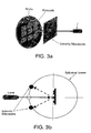
- the incident beam passes through an opening made on a flat screen where the light reflected by the wafer is viewed (figure 3).
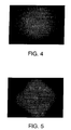
- the pattern of reflectance observed when analyzing a wafer without texture is a central point with circular symmetry (figure 4) due to the spreading of the light over the ruggedness and surface defects of the wafer.
- the pattern of optical reflectance of the wafers with a high degree of texture is a central point as mentioned, but appearing with less intensity and accompanied by four circular areas with order four symmetry in relation to the direction of the incoming beam (figure 5). This last reflectance pattern is due to the reflection on the four side faces of the pyramids.
- the method and the device of the present patent are both applicable to those texture morphologies characterized by the development of correlated geometrical patterns on the surface of the substrate that supports the photovoltaic cell. These patterns may have individual dimensions and distances between two consecutive patterns that may be random or constant, but in all cases the faces of all the polyhedral shapes that make them up must be mutually parallel. These morphologies may be formed by several procedures, such as the chemical etching of the monocrystalline Si, whether with raised or inverted pyramids. The method described may also be used for the study of other degrees of texture developed in multicrystalline Si and the texture present in polycrystalline silicone deposited over previously textured substrates with the aforementioned conditions. It can also be applied to other materials presenting similar texturing patterns.
- the method entails determining the pattern of reflectance associated to a textured surface (particularly those Si surfaces that have been subject to chemical etching to attain pyramidal shapes) that is originated by the light of a laser beam with normal incidence.
- This pattern is captured on a flat screen as shown on Figure 3a.
- the expected pattern for a surface composed of equal pyramid shapes would be composed of four points symmetrically located around the axis of the incoming beam, however, the presence of defects, non-textured areas, etc., causes an increase of the normal reflectance in detriment of the intensity associated to the texturing, which is the bases of the present method.
- FIGS. 3a and 3b show some of the alternatives that include spherical or semi-spherical screens, in which the wafer is placed in the middle and ellipsoid of revolution type screens in which the incoming beam passes through a focus point and the wafer, appropriately oriented, is located on the other of the foci of the ellipsoid. All these designs share a common characteristic.
- the beam reflected on the normal overlaps the incoming beam and therefore, makes difficult the measuring of the light reflected on the normal to the wafer. A technical solution to this problem is described further into the text.
- the measure of the degree of texture is obtained by comparing the intensity of the reflectance pattern with order four symmetry against the intensity exhibited in normal reflectance. To do this, it is necessary to place photodiodes over the screen and in the position of the maximums to register the intensity of the light. In a more elaborate version, detection may be done by means of a CCD detector or by a photodiode matrix distributed over the screen.
- a low power monomode laser ⁇ 10 mW
- good collimation properties typically 1.5 mRad or lower
- the reflectance patterns corresponding to intermediate texture patterns exhibit the maximum intensity with a symmetry that corresponds to the number of faces of the geometries that make up the texture, although they may appear joined by bands of lesser intensity. This situation may be appreciated in the image that corresponds to the reflection of a wafer treated during 25 minutes, as shown in Figure 5, formed by a four-faced pyramid.
- the parameter is not sensitive to the fluctuations of intensity of the laser beam.
- Deviation from parameter ⁇ n from its mean value, ⁇ n ⁇ , indicates lack of uniformity in the texture.
- the system described so far enables us to analyze the average area irradiated by the laser beam, typically ⁇ 0.5 x 0.5 mm 2.
- a bi-dimensional analysis of the wafer is required. Wafers typically have a round shape with a 15 cm diameter. This analysis may be done by a xy scan of the wafer, by moving the wafer, or by moving the optic system used for the projection, however, the mobile elements complicate the design and require, in the long term, re-calibration and maintenance.
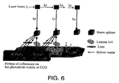
- the device described below minimizes the mobile elements and allows for the simultaneous analysis of several points in the wafer while said wafer moves over a conveyor belt in the y direction ( Figure 6).
- Analysis of the direction of movement is done by activating the measuring system at a constant time interval that is related to the wafer's speed of movement
- the x direction analysis is done simultaneously at several points within the wafer by means of dividing the initial laser beam into several beams of equal intensity vertically aimed (z-direction) towards the wafer.
- the laser beam radiation is linearly polarized.
- the laser beam with an initial intensity of I o propagating in x direction is split into several secondary beams of equal intensities l o r 1 aimed towards the z- direction.
- r n r n ⁇ 1 1 ⁇ r n 1
- a second set of polarization-sensitive beam divisors combined with ⁇ /4 sheets allows us to redirect the light reflected towards the detectors.
- the incoming beam hitting the second set of beam divisors must linearly polarized in the y-direction and in such a manner that it can be transmitted by the beam splitter.
- the ⁇ /4 sheet properly oriented with its axis at a 45° angle from the xy axis converts the light into circularly polarized light, and after reflecting from the wafer and going through a new transmission in the sheet the light emerges linearly polarized in the x- direction, and therefore it is totally reflected by the polarizing beam splitter in the y-direction.
- a lens collimates the image in order to project it onto the detector matrix where the intensity of the reflected beams is detected by the photodiodes and analyzed according to the previously described criteria. It is recommended to isolate the optical detection system from the ambient luminosity with interferential filters optimized to the wavelength and emission range of the laser utilized in the procedure and placed the filters in front of the photodiode matrix,
- Figure 7 presents a comparison of the angular distribution of the light's intensity reflected by an untreated monocrystalline Si (100) wafer and the distribution of a wafer treated in a 5 dm 3 aqueous solution of NaOH and i-C 3 H 7 OH.
- the light intensity measurements have been done at various ⁇ angles. This angle is varied on the plane containing the incoming light beam and is perpendicular to the wafer's surface and parallel to one of the sides of the pyramids' base.
- ⁇ 0
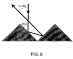
- there are two lateral maximums observed at 0 22°, that correspond to the beams reflected twice in the sides of the pyramids as shown in Figure 8.
- a beam splitter typically a beam-splitter cube.
- the minimum dimensions of said beam-splitter cube are conditioned by the separation angle between the reflected beams and the separation between the angle and the wafer.
- a collimating lens with a focal distance equal to the sum of the distances between the lens axis and the center of the beam splitter, and between the beam splitter and the wafer.
- all the optical elements used have anti-reflectant coatings with the same wavelength as that of the laser used during the procedure.
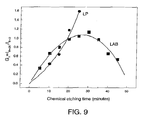
- the results obtained in the production line (PL) using baths of a similar chemical composition but in larger dimensions are also included. It is observed that there is a critical time period needed to reach the maximum degree of texture and that time periods that exceed said critical time period cause the flattening of the pyramids inducing the decrease of the G parameter.
- the results of the wafers treated at the production line in highly clean conditions reach greater G values than those obtained during the trial baths. The kinetics of the process is probably different, and this, together with the impossibility of exceeding the treatment time during the production process has prevented the observation of the maximum.
Landscapes
- Physics & Mathematics (AREA)
- General Physics & Mathematics (AREA)
- Health & Medical Sciences (AREA)
- Life Sciences & Earth Sciences (AREA)
- Chemical & Material Sciences (AREA)
- Analytical Chemistry (AREA)
- Biochemistry (AREA)
- General Health & Medical Sciences (AREA)
- Immunology (AREA)
- Pathology (AREA)
- Testing Or Measuring Of Semiconductors Or The Like (AREA)
- Investigating Materials By The Use Of Optical Means Adapted For Particular Applications (AREA)
- Investigating Or Analysing Materials By Optical Means (AREA)
- Photovoltaic Devices (AREA)
- Hybrid Cells (AREA)
- Silicon Compounds (AREA)
Abstract
Description
- This invention is related to the production engineering industry, and more particularly to the sector concerned with the production of photovoltaic cells, and therefore it also has a bearing on the alternative energy sector. The invention relates to the control of the methods used for texturing the surface of monocrystalline silicon, although it is also applicable to the textures developed on the surface of silicon and other multicrystalline and polycrystalline semiconductors.
- Decreasing the optical reflectance of the photosensitive side of the cell is an essential step of the manufacturing process necessary to improve the efficiency with which the photovoltaic cell converts the incident light into electric power. This is achieved by applying anti-reflectant coatings and inducing a well defined texture on the surface of the cell. Frequently, these two effects are achieved consecutively.
- During the texture forming process the cell develops a rough surface morphology [1,2], a porous or cavity-ridden morphology [3,4], or a faceted morphology [5] that allows multiple reflections on the surface before the light escapes irretrievably to the incident media (typically air or a transparent coating) and that additionally traps the long wave light by means of a total internal reflection (infrared light close to the Si gap) that penetrates in the active boundary area.
- Due to the high cost of crystalline materials, industrial production of photovoltaic cell technology is focused on silicon substrates (Si), although several crystalline quality grades are used. The highest quality cells use monocrystalline silicon (c-Si). Multicrystalline silicon (mc-Si), in which several crystalline grains have the same orientation, is also used. Currently, there is a great ongoing effort to improve the performance of thin sheets of polycrystalline silicon (p-Si). The methods used to texture the three different types of Si are also different.
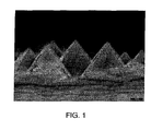
- The usual method to develop texture in monocrystalline silicon wafers is chemical surface treatment or etching, consisting in immersing the wafers in caustic baths that attack certain silicon crystalline planes preferentially [6,7], producing a random distribution of pyramid-shaped structures with a square base (figs.1 and 2), where all the pyramids present mutually parallel faces. This particular shape of the pyramids is caused by silicon's cubic symmetry and the appearance of planes (111) induced by the preferential chemical etching processes. Typically, when the degree of texture is high, the side of the pyramid's base is 5-10 µm and the tilt angle of the pyramid's lateral sides in relation to the substrate surface (α) is close to, but smaller than the cutting angle between the planes (111) and (100), or 54.735°. The tilt α depends slightly on the details of the chemical etching process that generates the texture and the values observed range from α = 49 -53°. This type of texture appears independently of the chemical agent used for the etching process that can be NaOH [7]. Na3P04:12H20 [8] or Na2C03 [9]. A variation of this texturizing method is the formation of inverted pyramids [10], although in this particular case the geometry of the texture is periodical and can be pre-determined by the manufacturer by means of a lithographic process.
- To characterize the anti-reflectant coatings, the techniques and instruments used (spectrophotometers, interferometers and ellipsometers) are based in optical methods that allow the evaluation without establishing physical contact with the cell, however, the study of the surface's texture is usually done by scanning electron microscopy (SEM) or with a profilometer and a scanning force microscope (SFM) with or without contact. Aside from the cost incurred in the utilization of these techniques, their adaptations to the industry as a quality control system of the cell's texture present certain difficulties. The scanning electron microscopy (SEM) requires a low pressure environment around the cell to work and the analyzed area may sustain damages due to the incidence of the electron beam. Also, the time required to perform the analysis considerably exceeds the speed of processing required for the production process. The profilometers, on the other hand, either work in contact mode, which may scratch the cell, or in optical mode that, while without contact, is developed to work on flat surfaces and do not adapt well to rugged and faceted surfaces because the reflectance is non-specular. The analysis time required both for scanning electron microscopy and for profilometry is in the order tens of minutes and therefore significantly longer than the time required for the individual analysis of cells in the production line (which is in the order of seconds).
- There is prior research work that has focused on the optical reflectance of textured photovoltaic cells [11, 12]. These papers report either an integral measurement of the total or diffuse reflectance or measures of specular reflectance even with normal incidence. The source of collimated light used is a HeNe laser with spectral coherence. For measurements concerned with non-coherent light a quartz lamp is used as source and the beam is focused (non-collimated). Ignoring some effects observed in periodical textures [11] and that are associated to the interference of the multiple beams associated to the HeNe laser coherence, the patterns of optical intensity analyzed in these works have a circular symmetry around the measurement axis [11]. The goal of these works is not to analyze the degree of texturization (which is known beforehand), but to evaluate the light-trapping efficacy of the texture.
- The objective of the method invented and the proposed devices resides in the development of a non-contact method for the quantitative analysis of the degree of texture in Si wafers that is suitable for implementation in the production line. It is mainly geared to the study or random texturization, although it is applicable to textures exhibiting periodicity. It is, therefore, a measuring instrument with a high level of performance that enables the user to accurately and instantaneously know the degree of texture of each individual cell immediately after the chemical etching process. The early detection of cells with a low degree of texturization allows for re-processing, avoiding having to reject them later and therefore avoiding the associated production costs of such an action. The method is based in the analysis of the reflectance of a beam of collimated light, without the light having to have a high spectral coherency, which makes the use of a laser source not essential, although the use of a laser source of light is advisable for practical purposes.
- The optimal formation of the aforementioned pyramids depends on several factors, such as temperature, pH of the bath solution, immersion times and the location of the wafers in the bath, as well as the initial state of the surface of the wafer amongst other factors. The degree of ageing of the bath also plays a fundamental role. Because the effect of the chemical etching process is not cumulative, but reaches a degree of maximum texture (maximum wafer area covered by pyramids) after which these pyramids are later flattened and disappear, the early detection of the decrease in texture allows us to know at every given moment, the status of the chemical baths used for their development, and therefore, we can take appropriate action before their degradation is obvious when inspecting the final product. In this manner two objectives would be achieved: one would be to lengthen the life of the baths by means of controlled addition of the necessary components, and the other would be to avoid the introduction in the production line of wafers with an intermediate degree of texturing that would result in efficiencies below the optimum expected at the end of the process.
-
- [1] K. Fukui, Y. Okada, H. Inomata, S. Takahashi, Y. Fujii, Fukawa and K. Shirasawa:
- "Surface and bulk-passivated large area multicrystalline silicon solar cells." Solar Energy Materials & Solar Cells: 48,219-228 (1997).
- [2] W.A. Nositschka, C. Beneking, O. Voigt and H. Kurz: "Texturisation of multicrystalline silicon wafer for solar cells by reactive ion etching through colloidal masks." Solar Energy Materials & Solar Cells: 76, 155-166 (2003).
- [3] Y. Yerokhov, R. Hezel, M. Lipinski, R. Ciach, H. Nagel, A. Mylyanych and P. Panek: "Cost-effective methods of texturing for silicon solar cells." Solar Energy Materials & Solar Cells: 72, 291-298 (2002).
- [4] J. Zhao, A. Wang, M.A. Green and F. Ferraza: "19.8% efficient "honeycomb" textured multicrystalline and 24.4% monocrystalline silicon solar cells." Applied Physics Letters: 73, 1991-1993 (1998).
- [5] P. Campbell and M.A. Green: "High performance light trapping textures for monocrystalline silicon solar calls." Solar Energy Materials & Solar Cells: 65, 369-375 (2001).
- [6] Holdermann, K: "Method for the wet chemical pyramidal texture etching of silicon surfaces." US Patent N° 6,451,218.
- [7] Bailey W.L., Coleman, M.G. Harris, C.B. Lesk and I.A. Lesk: "Texture etching of silicon: method." US Patent N° 4,137,123.
- [8] Z. Xi, D. Yang and D. Que: "Texturization of monocrystalline silicon with tribasic sodium phosphate." Solar Energy Materials & Solar Cells: 77, 255-263 (2003).
- [9] Y. Nishimoto and K. Namba: "Investigation of texturization for crystalline silicon solar cells with sodium carbonate solutions." Solar Energy Materials & Solar Cells: 61, 393 - 402 (2000).
- [10] W. Müller, A. Metz and R. Hezei: "A new and simple approach for fabricating inverted pyramids on crystalline silicon solar cells." Proceedings of the 17th European Photovoltaic Solar Energy Conference, Munich (2001).
- [11] A. Paretta, E. Bobeico, L. Lancellotti, P. Morvillo, A. Wang and J. Zhao: "A new approach to the analysis of light collected by textured silicon surfaces." Paper 1P- C3 -14 in the 3rd World Conference on Photovoltaic Energy Conversion, Osaka, May 12-16 (2003).
- [12] A. Paretta, A. Sarno, P. Tortota, H. Yakubu, P. Maddalena, J. Zhao and A. Wang: "Angle-dependent reflectance measurements on photovoltaic materials and solar cells." Optical Communications 172, 139-151 (1999).
- The authors claim the invention of a Method and a device to determine the degree of texturization of materials, amongst others, the silicon wafers typically used as photovoltaic cells.
- The technique proposed to establish the degree of texturization consists, basically, in irradiate the wafer's surface with a collimated light beam and quantify the patterns of optical reflectance. In the following text we will refer to laser light as the source for this process because of their generally good collimation properties, without intending to communicate by it that the coherent character of the laser light has a decisive influence on the present invention.
- In the simplest assembly, the incident beam passes through an opening made on a flat screen where the light reflected by the wafer is viewed (figure 3). The pattern of reflectance observed when analyzing a wafer without texture is a central point with circular symmetry (figure 4) due to the spreading of the light over the ruggedness and surface defects of the wafer. The pattern of optical reflectance of the wafers with a high degree of texture is a central point as mentioned, but appearing with less intensity and accompanied by four circular areas with order four symmetry in relation to the direction of the incoming beam (figure 5). This last reflectance pattern is due to the reflection on the four side faces of the pyramids. Proof of this is that when the wafer is rotated on the axis established by the incoming laser beam, the reflected pattern rotates in solidarity with the wafer. It should be noted that the light reflected by the wafer does not exhibit significant polarization changes in relation to the incoming light and that the angular opening of the pattern of light reflected is not sensitive to the wavelength of the light used, which would demonstrate that it is associated to specular reflections on the microscopic facets of the sample.
- The method and the device of the present patent are both applicable to those texture morphologies characterized by the development of correlated geometrical patterns on the surface of the substrate that supports the photovoltaic cell. These patterns may have individual dimensions and distances between two consecutive patterns that may be random or constant, but in all cases the faces of all the polyhedral shapes that make them up must be mutually parallel. These morphologies may be formed by several procedures, such as the chemical etching of the monocrystalline Si, whether with raised or inverted pyramids. The method described may also be used for the study of other degrees of texture developed in multicrystalline Si and the texture present in polycrystalline silicone deposited over previously textured substrates with the aforementioned conditions. It can also be applied to other materials presenting similar texturing patterns.
- As described above, the method entails determining the pattern of reflectance associated to a textured surface (particularly those Si surfaces that have been subject to chemical etching to attain pyramidal shapes) that is originated by the light of a laser beam with normal incidence. This pattern is captured on a flat screen as shown on Figure 3a. According to the laws of reflection, the expected pattern for a surface composed of equal pyramid shapes would be composed of four points symmetrically located around the axis of the incoming beam, however, the presence of defects, non-textured areas, etc., causes an increase of the normal reflectance in detriment of the intensity associated to the texturing, which is the bases of the present method.
- The geometry of the screen may be adapted to the circumstances of the design. Figures 3a and 3b, respectively, show some of the alternatives that include spherical or semi-spherical screens, in which the wafer is placed in the middle and ellipsoid of revolution type screens in which the incoming beam passes through a focus point and the wafer, appropriately oriented, is located on the other of the foci of the ellipsoid. All these designs share a common characteristic. The beam reflected on the normal overlaps the incoming beam and therefore, makes difficult the measuring of the light reflected on the normal to the wafer. A technical solution to this problem is described further into the text.
- The measure of the degree of texture is obtained by comparing the intensity of the reflectance pattern with order four symmetry against the intensity exhibited in normal reflectance. To do this, it is necessary to place photodiodes over the screen and in the position of the maximums to register the intensity of the light. In a more elaborate version, detection may be done by means of a CCD detector or by a photodiode matrix distributed over the screen. The light source may be a low power monomode laser (< 10 mW) and good collimation properties (typically 1.5 mRad or lower) emitting in the region of A = 500 - 800 nm, typically a HeNe laser (A = 633 nm), of a semiconductor diode (A = 750 - 850 nm) with collimating optics, or one of these lasers with infrared emission (A 1060 nm), or Nd3+ (λ ≈ 1060 nm), in both cases in conjunction with a frequency doubler.
- The reflectance patterns corresponding to intermediate texture patterns exhibit the maximum intensity with a symmetry that corresponds to the number of faces of the geometries that make up the texture, although they may appear joined by bands of lesser intensity. This situation may be appreciated in the image that corresponds to the reflection of a wafer treated during 25 minutes, as shown in Figure 5, formed by a four-faced pyramid.
- To characterize the degree of texture of the surface, the G parameter is defined as the relation between the sum of the intensities reflected in the maximums of the pattern with four order symmetry I 4n (n = 1 - 4), and the intensity normally reflected to the surface of the wafer I N

- This is a non-linear function that ideally has a value of zero for the wafer without texture and a value of infinite for a wafer with perfect texture, although its value is limited by the overlapping between the patterns with circular symmetry and the patterns exhibiting order four symmetry The parameter is not sensitive to the fluctuations of intensity of the laser beam.
- There is a second set of parameters to characterize the uniformity of the texture:

- Deviation from parameter χ n from its mean value,


for each value of n. - The system described so far enables us to analyze the average area irradiated by the laser beam, typically < 0.5 x 0.5 mm2. To incorporate the system to the production line a bi-dimensional analysis of the wafer is required. Wafers typically have a round shape with a 15 cm diameter. This analysis may be done by a xy scan of the wafer, by moving the wafer, or by moving the optic system used for the projection, however, the mobile elements complicate the design and require, in the long term, re-calibration and maintenance. The device described below minimizes the mobile elements and allows for the simultaneous analysis of several points in the wafer while said wafer moves over a conveyor belt in the y direction (Figure 6).
- Analysis of the direction of movement is done by activating the measuring system at a constant time interval that is related to the wafer's speed of movement The x direction analysis is done simultaneously at several points within the wafer by means of dividing the initial laser beam into several beams of equal intensity vertically aimed (z-direction) towards the wafer.
- In this particular instance, it is necessary that the laser beam radiation is linearly polarized. The laser beam with an initial intensity of I o propagating in x direction is split into several secondary beams of equal intensities l o r 1 aimed towards the z- direction. To do this several N beam splitters not-sensitive to the polarization of the incoming light are used and calibrated so their reflectivity r n fulfils the following relationship:


- A second set of polarization-sensitive beam divisors combined with λ/4 sheets allows us to redirect the light reflected towards the detectors. The incoming beam hitting the second set of beam divisors must linearly polarized in the y-direction and in such a manner that it can be transmitted by the beam splitter. The λ/4 sheet properly oriented with its axis at a 45° angle from the xy axis converts the light into circularly polarized light, and after reflecting from the wafer and going through a new transmission in the sheet the light emerges linearly polarized in the x- direction, and therefore it is totally reflected by the polarizing beam splitter in the y-direction. Finally, a lens (previously mentioned) collimates the image in order to project it onto the detector matrix where the intensity of the reflected beams is detected by the photodiodes and analyzed according to the previously described criteria. It is recommended to isolate the optical detection system from the ambient luminosity with interferential filters optimized to the wavelength and emission range of the laser utilized in the procedure and placed the filters in front of the photodiode matrix,
-
- Figure 1
- Image obtained by scanning electron microscopy of the squared-based pyramids after chemical etching with NaOH. The angle formed between the pyramid's side faces is calculated from the image and the tilt of the faces in relation to the wafer's plane coincides, within the experimental uncertainty range, with the expected values between planes (111)Si and the planes (111)Si-(100) Si, 70.53° and 54.73° respectively.
- Figure 2
- Shows the zenithal image obtained by scanning electro microscopy of the square-based pyramids resulting from the chemical etching with NaOH. As observed, all the pyramids exhibit the same orientation, which makes the reflectance pattern be formed by four points symmetrically placed around the illumination axis.
- Figure 3a
- Simple outline of a reflectance pattern observation device on the textured silicon surfaces by means of a flat display.
- Figure 3b
- Simple outline of a reflectance pattern observation device on the textured silicon surfaces by means of a spherical display. The image in the figure shows a cross section.
- Figure 3c
- Simple outline of a reflectance pattern observation device on the textured silicon surfaces by means of an ellipsoid of revolution display that acts internally as a reflector. The image in the figure shows a cross section.
- Figure 4
- Optical reflectance pattern of a non-textured (100) Si surface. The circular symmetry around the most intense central point can be observed. This point corresponds to the incoming light beam.
- Figure 5
- Optical reflectance pattern of a highly textured (100) Si surface. The order four symmetry around the most intense central point can be observed. This point corresponds to the incoming light beam.
- Figure 6
- Outline of the device proposed for the optical characterization of the degree of texture in the (100) Si wafers.
- Figure 7
- Comparison between the angular distribution of the intensity of the light reflected by a wafer (100) c-Si before the chemical etching process that originates the surface texture (t = 0 min), and that of texture obtained in a sample subject to the etching process during 25 min., where 0 is the observation angle in relation to the normal of the wafer's surface, expressed in degrees.
- Figure 8
- Outline of the multiple reflections of a light ray with normal incidence over a textured surface of the (100) Si.
- Figure 9
- Evolution of the texture parameter G incorporating the time it takes to chemically process the (100) c-Si wafers in an aqueous solution of NaOH and i-C3H7OH. The wafers marked "LAB" have been textured in trial baths while the ones marked as "PL" have been textured in the production line of a solar cell manufacturing facility.
- Following the proposed method of measuring the reflectance pattern, Figure 7 presents a comparison of the angular distribution of the light's intensity reflected by an untreated monocrystalline Si (100) wafer and the distribution of a wafer treated in a 5 dm3 aqueous solution of NaOH and i-C3H7OH. The light intensity measurements have been done at various θ angles. This angle is varied on the plane containing the incoming light beam and is perpendicular to the wafer's surface and parallel to one of the sides of the pyramids' base. In addition to a central maximum (θ = 0) that is present even in the non-textured wafers, there are two lateral maximums observed at 0 = 22°, that correspond to the beams reflected twice in the sides of the pyramids as shown in Figure 8.
- According to this figure, the angle of reflectance in relation to the incoming beam (θ) is related to the inclination or tilt (α) of the pyramid's side as shown by the relation θ = 4α- 180°. It has been observed that the
angular gap 20 between the non-specular reflectance varies in the 40-52° range as a function of the quality of the texture induced during the chemical etching process. This variation is associated to certain dispersion in the value of α and could be related either to the presence of stagger or any other defects present on the pyramid's faces, or to the crystalline quality of the starting substrate. - To implement the system it is necessary to evaluate the intensity of the reflected light beam parallel to the incoming beam, as well as the intensity of the beams reflected in the maximums when they have an approximate value of 22°. This is resolved by using a beam splitter, typically a beam-splitter cube. The minimum dimensions of said beam-splitter cube are conditioned by the separation angle between the reflected beams and the separation between the angle and the wafer. To project the light pattern over the optical detection system, it is advisable to incorporate a collimating lens with a focal distance equal to the sum of the distances between the lens axis and the center of the beam splitter, and between the beam splitter and the wafer. To avoid undesired image in the detectors' plane it is necessary that all the optical elements used (beam splitters, lenses, retardant film or sheets, detectors, etc) have anti-reflectant coatings with the same wavelength as that of the laser used during the procedure.
- Figure 9 shows a simplified version of the G n=I θ=26 / I θ=0 parameter as a function of the time of chemical etching process for a scan done on the plane

- Although the example just described refers to four sided pyramidal geometries, this does not imply that the method is restricted solely to that type of geometry, since it is essentially valid for other geometrical figures (n-side pyramids, cones, etc.) that can also form on the Si surface, whether by chemical etching or other type of processes.
Claims (4)
- A process to establish the degree of surface texture of wafers of semiconductor material, and specifically of monocrystalline or multicrystalline silicon wafers, characterized in that:a. it uses a new set of mathematical parameters:

where I4n (n =I-4) is the intensity of the light reflected to a given angle separated from the normal, and IN is the intensity normally reflected to the wafer's surface,
and b. it relates the intensity of the laser beam light reflected to a solid angle, whether centered or separated from the laser beam's angle of incidence, with the degree of textured filling on the surface of the wafer of the material analyzed;c. it establish the degree of texture of the wafer's surface by means of analyzing the maximums in the pattern of intensity of the reflected laser beam light;d. it enables the simultaneous and non-destructive analysis of the texture in several different points on the wafer's surface;e. it uses the rotation of the polarization of the sampling beam to separate the reflected beams from the incident beam.
 - Procedure to measure the intensity of the reflectance pattern of the wafer's surface according to claim 1, and characterized in that the analysis of the reflected image obtained when the wafer is illuminated with a laser beam light on screens of various geometries:a. flat screen placed parallel to the wafer;b. wafer-centered spherical or hemispherical screen;c. ellipsoid of revolution-shaped screen with the wafer placed at one of the foci and the beam passing through the opposite one.
- Procedure to analyze the measurement of reflection patterns according to claims 1 and 2, and applicable, amongst other, to monocrystalline silicon wafers, and characterized in that:a. it associates the reflections with n-order symmetry n (n = 3, 4, 6...) to the presence of geometrical structures located on the surface of the wafer, preferably a silicon wafer, with this same symmetry;b. it defines a method to measure the angle formed by the wafer's surface and the faces of the geometrical structures that form the texture;c. it relates the angular width of the reflectance maximums to the presence of defects on the geometrical structures that form the texture and to the degree of multicrystallinity of the starting substrate;d. it obtains and defines the existence of an optimum degree of texture related to the time of chemical processing and to the appearance of a reflectance maximum at θ 26 - 20° for the same processing time;e. it associates the relationship between the intensities of the light normally reflected (θ = 0°) and light reflected at θ 26- 20°, with the degree of texture associated to silicon planes (111);f. it associates the optical reflection angle 0 with the average tilt of the sides of the pyramids that form the surface texture.
- Device for carrying out the procedure of claims 1, 2, and 3 that allows the simultaneous non-invasive and non-destructive analysis of the degree of texture of several points of the wafer and also the re-aiming of the reflected light in a direction spatially separated from the incident beam and that is characterized in that:a. it uses a set of unpublished mathematical parameters as defined in claim 1, that characterize the total degree and uniformity of the texture and serve to establish the surface texture of the wafers, allowing in turn to determine the correlation between the degree of texture of the wafer's surface with the intensity maximums present on the reflected light pattern;b. it relates the intensity of a laser beam light reflected at a solid angle, centered or separated from the incidence of the laser beam axis, to the degree of textured filling on the surface of the wafer of the analyzed material;c. it establishes the degree of texture of the wafer's surface by means of analyzing the intensity of the maximums present in the pattern of reflection of the laser beam light;d. it allows for the simultaneous analysis of the texture at various different points located on the wafer's surface by designing the reflectance of the optic elements utilized to split the beam;e. it utilizes the rotation of the polarization of the sampling beam together with the optic elements sensitive to the polarization status to separate the reflected beams from the incident beam;f. it analyzes the reflection image obtained on a flat screen placed perpendicularly from the wafer when the wafer is illuminated by a laser beam light;g. it associates the reflections with order-n symmetry n (n = 3, 4, 6...) to the presence of geometric structures on the surface of the wafer, particularly on silicon wafers exhibiting that same symmetry;h. it measures the angle formed by the wafer's surface and the faces of the geometric shapes that form the texture;i. it relates the angular width of the reflection maximums to the order four symmetry and to the degree of multicrystallinity of the starting substrate;j. it measures and obtaines the relationship between the intensity of light reflected normally (θ = 0°) and at 0 26 - 20° with the degree of texture associated to silicon planes (111);k, it measures the optical reflection angle θ associated to the average tilt of the faces of the pyramids that form the surface texture.
Applications Claiming Priority (2)
| Application Number | Priority Date | Filing Date | Title |
|---|---|---|---|
| ES200301666A ES2235608B1 (en) | 2003-07-15 | 2003-07-15 | OPTICAL AND DEVICE METHOD FOR THE QUANTIFICATION OF TEXTURE IN PHOTOVOLTAIC CELLS. |
| PCT/ES2004/070050 WO2005008175A1 (en) | 2003-07-15 | 2004-07-14 | Optical method and device for texture quantification of photovoltaic cells |
Publications (2)
| Publication Number | Publication Date |
|---|---|
| EP1662227A1 true EP1662227A1 (en) | 2006-05-31 |
| EP1662227B1 EP1662227B1 (en) | 2007-06-13 |
Family
ID=34072908
Family Applications (1)
| Application Number | Title | Priority Date | Filing Date |
|---|---|---|---|
| EP04742088A Expired - Lifetime EP1662227B1 (en) | 2003-07-15 | 2004-07-14 | Optical method and device for texture quantification of photovoltaic cells |
Country Status (8)
| Country | Link |
|---|---|
| US (1) | US20060268283A1 (en) |
| EP (1) | EP1662227B1 (en) |
| JP (1) | JP2007528997A (en) |
| CN (1) | CN100419377C (en) |
| AT (1) | ATE364830T1 (en) |
| DE (1) | DE602004007014T2 (en) |
| ES (1) | ES2235608B1 (en) |
| WO (1) | WO2005008175A1 (en) |
Cited By (1)
| Publication number | Priority date | Publication date | Assignee | Title |
|---|---|---|---|---|
| WO2011144374A1 (en) * | 2010-05-19 | 2011-11-24 | Robert Bosch Gmbh | Method and device for characterising pyramidal surface structures on a substrate |
Families Citing this family (7)
| Publication number | Priority date | Publication date | Assignee | Title |
|---|---|---|---|---|
| US7742171B2 (en) * | 2007-08-06 | 2010-06-22 | Ci Systems Ltd. | Reflectivity/emissivity measurement probe insensitive to variations in probe-to-target distance |
| US8378661B1 (en) * | 2008-05-29 | 2013-02-19 | Alpha-Omega Power Technologies, Ltd.Co. | Solar simulator |
| GB0816047D0 (en) * | 2008-09-04 | 2008-10-08 | Rolls Royce Plc | Crystallographic orientation measurement |
| DE102009044458B4 (en) * | 2009-11-06 | 2021-03-04 | Hanwha Q.CELLS GmbH | Analysis method for analyzing a semiconductor wafer |
| DE102010011056A1 (en) | 2010-03-11 | 2011-09-15 | Jörg Bischoff | Method for measuring e.g. filling degree of mono-crystalline silicon wafer that is utilized in photovoltaic system, involves determining uniformity of facets from normalized difference of reflectance using predefined formula |
| JP2013002900A (en) * | 2011-06-15 | 2013-01-07 | Mitsubishi Electric Corp | Ellipsometer device and measuring method for anti-reflection film formed on mono-crystalline silicon |
| DE102012012156B4 (en) * | 2012-06-19 | 2014-05-15 | Audiodev Gmbh | METHOD OF OPTICALLY MEASURING PYRAMIDS ON TEXTURED MONOCRYSTALLINE SILICON WAFERS |
Family Cites Families (12)
| Publication number | Priority date | Publication date | Assignee | Title |
|---|---|---|---|---|
| US4137123A (en) * | 1975-12-31 | 1979-01-30 | Motorola, Inc. | Texture etching of silicon: method |
| JPS58140609A (en) * | 1982-02-17 | 1983-08-20 | Toshiba Corp | Evaluating device of surface condition |
| JPS58111743A (en) * | 1981-12-26 | 1983-07-02 | Toshiba Corp | Evaluating device for state of surface |
| JPH0739946B2 (en) * | 1987-08-26 | 1995-05-01 | 株式会社豊田中央研究所 | Surface condition inspection device |
| US6118525A (en) * | 1995-03-06 | 2000-09-12 | Ade Optical Systems Corporation | Wafer inspection system for distinguishing pits and particles |
| EP0979398B1 (en) * | 1996-06-04 | 2012-01-04 | KLA-Tencor Corporation | Optical scanning system for surface inspection |
| JP3257413B2 (en) * | 1996-09-10 | 2002-02-18 | 松下電器産業株式会社 | Laser processing apparatus and laser processing method |
| MY123792A (en) * | 1996-12-04 | 2006-06-30 | Ade Optical Systems | Wafer inspection system for distinguishing pits and particles |
| DE19811878C2 (en) * | 1998-03-18 | 2002-09-19 | Siemens Solar Gmbh | Process and etching solution for wet chemical pyramidal texture etching of silicon surfaces |
| SE514309C2 (en) * | 1999-05-28 | 2001-02-05 | Ericsson Telefon Ab L M | Method for determination of surface texture of injection moulded polymer, Al, Mn or Zn products measures two parameters of surface texture |
| US6778273B2 (en) * | 2001-03-30 | 2004-08-17 | Therma-Wave, Inc. | Polarimetric scatterometer for critical dimension measurements of periodic structures |
| WO2003054475A2 (en) * | 2001-12-19 | 2003-07-03 | Kla-Tencor Technologies Corporation | Parametric profiling using optical spectroscopic systems |
-
2003
- 2003-07-15 ES ES200301666A patent/ES2235608B1/en not_active Expired - Fee Related
-
2004
- 2004-07-14 JP JP2006519940A patent/JP2007528997A/en active Pending
- 2004-07-14 EP EP04742088A patent/EP1662227B1/en not_active Expired - Lifetime
- 2004-07-14 DE DE602004007014T patent/DE602004007014T2/en not_active Expired - Fee Related
- 2004-07-14 WO PCT/ES2004/070050 patent/WO2005008175A1/en not_active Ceased
- 2004-07-14 AT AT04742088T patent/ATE364830T1/en not_active IP Right Cessation
- 2004-07-14 CN CNB2004800263463A patent/CN100419377C/en not_active Expired - Fee Related
-
2006
- 2006-01-12 US US11/330,706 patent/US20060268283A1/en not_active Abandoned
Non-Patent Citations (1)
| Title |
|---|
| See references of WO2005008175A1 * |
Cited By (1)
| Publication number | Priority date | Publication date | Assignee | Title |
|---|---|---|---|---|
| WO2011144374A1 (en) * | 2010-05-19 | 2011-11-24 | Robert Bosch Gmbh | Method and device for characterising pyramidal surface structures on a substrate |
Also Published As
| Publication number | Publication date |
|---|---|
| JP2007528997A (en) | 2007-10-18 |
| CN100419377C (en) | 2008-09-17 |
| ES2235608A1 (en) | 2005-07-01 |
| EP1662227B1 (en) | 2007-06-13 |
| CN1871495A (en) | 2006-11-29 |
| WO2005008175A1 (en) | 2005-01-27 |
| DE602004007014D1 (en) | 2007-07-26 |
| ES2235608B1 (en) | 2006-11-01 |
| ATE364830T1 (en) | 2007-07-15 |
| US20060268283A1 (en) | 2006-11-30 |
| DE602004007014T2 (en) | 2008-02-14 |
Similar Documents
| Publication | Publication Date | Title |
|---|---|---|
| Baker‐Finch et al. | Reflection distributions of textured monocrystalline silicon: implications for silicon solar cells | |
| Forniés et al. | Control of random texture of monocrystalline silicon cells by angle-resolved optical reflectance | |
| Iyengar et al. | Optical properties of silicon light trapping structures for photovoltaics | |
| US7502104B2 (en) | Probe beam profile modulated optical reflectance system and methods | |
| CN101128835B (en) | Shape roughness measurement in optical metrology | |
| EP1662227B1 (en) | Optical method and device for texture quantification of photovoltaic cells | |
| CN101276010B (en) | Diffraction optics element scan etching device with etch deepness on-line detection mechanism | |
| CN101377413B (en) | Method for measuring photoresist mask slot-shaped structure parameter | |
| WO1996010171A1 (en) | System for characterizing semiconductor materials and photovoltaic devices | |
| Mennucci et al. | Light scattering properties of self-organized nanostructured substrates for thin-film solar cells | |
| JP2000031229A (en) | Semiconductor thin film inspection method and semiconductor thin film manufacturing method using the same | |
| Jäger et al. | Angular resolved scattering measurements of nano-textured substrates in a broad wavelength range | |
| Hashmi et al. | Texturization of as-cut p-type monocrystalline silicon wafer using different wet chemical solutions | |
| Saenger et al. | Spectroscopic ellipsometry characterization of SiNx antireflection films on textured multicrystalline and monocrystalline silicon solar cells | |
| AU2004299652B2 (en) | Measuring pyramid size on a textured surface | |
| US8248607B1 (en) | Empirical correction for spectroscopic ellipsometric measurements of rough or textured surfaces | |
| Zaldo et al. | Optical method and device for texture quantification of photovoltaic cells | |
| Hein et al. | Glass surface modification by lithography-free reactive ion etching in an Ar/CF4-plasma for controlled diffuse optical scattering | |
| CN110196240B (en) | Method for measuring refractive index and thickness of thin film through laser modification based on PL interference phenomenon | |
| Parretta et al. | A new approach to the analysis of light collected by textured silicon surfaces | |
| Razi et al. | Angle-and polarization-dependent reflection and backscattering from FS-LIPSS covered stainless steel surfaces: experimental study | |
| Kuo et al. | Rapid optical measurement of surface texturing result of crystalline silicon wafers for high efficiency solar cells application | |
| Bobeico et al. | ANALYSIS OF LIGHT BACKSCATTERED FROM TEXTURED SILICON SURFACES | |
| Hatfield et al. | Surface Treatment Regimes for Solar Scatter Control in Millimeter Wave Telescope Panels | |
| Kolesar et al. | Optical scattering enhanced by silicon micromachined surfaces |
Legal Events
| Date | Code | Title | Description |
|---|---|---|---|
| PUAI | Public reference made under article 153(3) epc to a published international application that has entered the european phase |
Free format text: ORIGINAL CODE: 0009012 |
|
| 17P | Request for examination filed |
Effective date: 20060215 |
|
| AK | Designated contracting states |
Kind code of ref document: A1 Designated state(s): AT BE BG CH CY CZ DE DK EE ES FI FR GB GR HU IE IT LI LU MC NL PL PT RO SE SI SK TR |
|
| DAX | Request for extension of the european patent (deleted) | ||
| GRAP | Despatch of communication of intention to grant a patent |
Free format text: ORIGINAL CODE: EPIDOSNIGR1 |
|
| GRAS | Grant fee paid |
Free format text: ORIGINAL CODE: EPIDOSNIGR3 |
|
| GRAA | (expected) grant |
Free format text: ORIGINAL CODE: 0009210 |
|
| RIN1 | Information on inventor provided before grant (corrected) |
Inventor name: FORNIES GARCIA, EDUARDO Inventor name: ZALDO LUEZAS, CARLOS ENRIQUE Inventor name: ALBELLA MARTIN, JOSE MARIA |
|
| RIN1 | Information on inventor provided before grant (corrected) |
Inventor name: ALBELLA MARTIN, JOSE MARIA Inventor name: ZALDO LUEZAS, CARLOS ENRIQUE Inventor name: FORNIES GARCIA, EDUARDO |
|
| AK | Designated contracting states |
Kind code of ref document: B1 Designated state(s): AT BE BG CH CY CZ DE DK EE ES FI FR GB GR HU IE IT LI LU MC NL PL PT RO SE SI SK TR |
|
| PG25 | Lapsed in a contracting state [announced via postgrant information from national office to epo] |
Ref country code: LI Free format text: LAPSE BECAUSE OF FAILURE TO SUBMIT A TRANSLATION OF THE DESCRIPTION OR TO PAY THE FEE WITHIN THE PRESCRIBED TIME-LIMIT Effective date: 20070613 Ref country code: CH Free format text: LAPSE BECAUSE OF FAILURE TO SUBMIT A TRANSLATION OF THE DESCRIPTION OR TO PAY THE FEE WITHIN THE PRESCRIBED TIME-LIMIT Effective date: 20070613 |
|
| REG | Reference to a national code |
Ref country code: GB Ref legal event code: FG4D |
|
| REG | Reference to a national code |
Ref country code: CH Ref legal event code: EP |
|
| REG | Reference to a national code |
Ref country code: IE Ref legal event code: FG4D |
|
| REF | Corresponds to: |
Ref document number: 602004007014 Country of ref document: DE Date of ref document: 20070726 Kind code of ref document: P |
|
| REG | Reference to a national code |
Ref country code: SE Ref legal event code: TRGR |
|
| PG25 | Lapsed in a contracting state [announced via postgrant information from national office to epo] |
Ref country code: PL Free format text: LAPSE BECAUSE OF FAILURE TO SUBMIT A TRANSLATION OF THE DESCRIPTION OR TO PAY THE FEE WITHIN THE PRESCRIBED TIME-LIMIT Effective date: 20070613 |
|
| ET | Fr: translation filed | ||
| REG | Reference to a national code |
Ref country code: CH Ref legal event code: PL |
|
| PG25 | Lapsed in a contracting state [announced via postgrant information from national office to epo] |
Ref country code: SI Free format text: LAPSE BECAUSE OF FAILURE TO SUBMIT A TRANSLATION OF THE DESCRIPTION OR TO PAY THE FEE WITHIN THE PRESCRIBED TIME-LIMIT Effective date: 20070613 Ref country code: PT Free format text: LAPSE BECAUSE OF FAILURE TO SUBMIT A TRANSLATION OF THE DESCRIPTION OR TO PAY THE FEE WITHIN THE PRESCRIBED TIME-LIMIT Effective date: 20071113 Ref country code: ES Free format text: LAPSE BECAUSE OF FAILURE TO SUBMIT A TRANSLATION OF THE DESCRIPTION OR TO PAY THE FEE WITHIN THE PRESCRIBED TIME-LIMIT Effective date: 20070924 Ref country code: BG Free format text: LAPSE BECAUSE OF FAILURE TO SUBMIT A TRANSLATION OF THE DESCRIPTION OR TO PAY THE FEE WITHIN THE PRESCRIBED TIME-LIMIT Effective date: 20070913 Ref country code: CZ Free format text: LAPSE BECAUSE OF FAILURE TO SUBMIT A TRANSLATION OF THE DESCRIPTION OR TO PAY THE FEE WITHIN THE PRESCRIBED TIME-LIMIT Effective date: 20070613 |
|
| PG25 | Lapsed in a contracting state [announced via postgrant information from national office to epo] |
Ref country code: SK Free format text: LAPSE BECAUSE OF FAILURE TO SUBMIT A TRANSLATION OF THE DESCRIPTION OR TO PAY THE FEE WITHIN THE PRESCRIBED TIME-LIMIT Effective date: 20070613 |
|
| PLBE | No opposition filed within time limit |
Free format text: ORIGINAL CODE: 0009261 |
|
| STAA | Information on the status of an ep patent application or granted ep patent |
Free format text: STATUS: NO OPPOSITION FILED WITHIN TIME LIMIT |
|
| PG25 | Lapsed in a contracting state [announced via postgrant information from national office to epo] |
Ref country code: MC Free format text: LAPSE BECAUSE OF NON-PAYMENT OF DUE FEES Effective date: 20070731 Ref country code: GR Free format text: LAPSE BECAUSE OF FAILURE TO SUBMIT A TRANSLATION OF THE DESCRIPTION OR TO PAY THE FEE WITHIN THE PRESCRIBED TIME-LIMIT Effective date: 20070914 Ref country code: DK Free format text: LAPSE BECAUSE OF FAILURE TO SUBMIT A TRANSLATION OF THE DESCRIPTION OR TO PAY THE FEE WITHIN THE PRESCRIBED TIME-LIMIT Effective date: 20070613 |
|
| 26N | No opposition filed |
Effective date: 20080314 |
|
| PG25 | Lapsed in a contracting state [announced via postgrant information from national office to epo] |
Ref country code: RO Free format text: LAPSE BECAUSE OF FAILURE TO SUBMIT A TRANSLATION OF THE DESCRIPTION OR TO PAY THE FEE WITHIN THE PRESCRIBED TIME-LIMIT Effective date: 20070613 |
|
| PGFP | Annual fee paid to national office [announced via postgrant information from national office to epo] |
Ref country code: DE Payment date: 20080829 Year of fee payment: 5 |
|
| PGFP | Annual fee paid to national office [announced via postgrant information from national office to epo] |
Ref country code: IE Payment date: 20080704 Year of fee payment: 5 Ref country code: IT Payment date: 20080722 Year of fee payment: 5 Ref country code: NL Payment date: 20080715 Year of fee payment: 5 Ref country code: AT Payment date: 20080724 Year of fee payment: 5 Ref country code: FR Payment date: 20080703 Year of fee payment: 5 |
|
| PGFP | Annual fee paid to national office [announced via postgrant information from national office to epo] |
Ref country code: GB Payment date: 20080716 Year of fee payment: 5 |
|
| PG25 | Lapsed in a contracting state [announced via postgrant information from national office to epo] |
Ref country code: EE Free format text: LAPSE BECAUSE OF FAILURE TO SUBMIT A TRANSLATION OF THE DESCRIPTION OR TO PAY THE FEE WITHIN THE PRESCRIBED TIME-LIMIT Effective date: 20070613 |
|
| PG25 | Lapsed in a contracting state [announced via postgrant information from national office to epo] |
Ref country code: FI Free format text: LAPSE BECAUSE OF FAILURE TO SUBMIT A TRANSLATION OF THE DESCRIPTION OR TO PAY THE FEE WITHIN THE PRESCRIBED TIME-LIMIT Effective date: 20070613 |
|
| PGFP | Annual fee paid to national office [announced via postgrant information from national office to epo] |
Ref country code: BE Payment date: 20080729 Year of fee payment: 5 Ref country code: SE Payment date: 20080707 Year of fee payment: 5 |
|
| PG25 | Lapsed in a contracting state [announced via postgrant information from national office to epo] |
Ref country code: CY Free format text: LAPSE BECAUSE OF FAILURE TO SUBMIT A TRANSLATION OF THE DESCRIPTION OR TO PAY THE FEE WITHIN THE PRESCRIBED TIME-LIMIT Effective date: 20070613 |
|
| PG25 | Lapsed in a contracting state [announced via postgrant information from national office to epo] |
Ref country code: LU Free format text: LAPSE BECAUSE OF NON-PAYMENT OF DUE FEES Effective date: 20070714 |
|
| PG25 | Lapsed in a contracting state [announced via postgrant information from national office to epo] |
Ref country code: HU Free format text: LAPSE BECAUSE OF FAILURE TO SUBMIT A TRANSLATION OF THE DESCRIPTION OR TO PAY THE FEE WITHIN THE PRESCRIBED TIME-LIMIT Effective date: 20071214 Ref country code: TR Free format text: LAPSE BECAUSE OF FAILURE TO SUBMIT A TRANSLATION OF THE DESCRIPTION OR TO PAY THE FEE WITHIN THE PRESCRIBED TIME-LIMIT Effective date: 20070613 |
|
| BERE | Be: lapsed |
Owner name: CONSEJO SUPERIOR DE INVESTIGACIONES CIENTIFICAS Effective date: 20090731 |
|
| EUG | Se: european patent has lapsed | ||
| GBPC | Gb: european patent ceased through non-payment of renewal fee |
Effective date: 20090714 |
|
| NLV4 | Nl: lapsed or anulled due to non-payment of the annual fee |
Effective date: 20100201 |
|
| REG | Reference to a national code |
Ref country code: FR Ref legal event code: ST Effective date: 20100331 |
|
| PG25 | Lapsed in a contracting state [announced via postgrant information from national office to epo] |
Ref country code: FR Free format text: LAPSE BECAUSE OF NON-PAYMENT OF DUE FEES Effective date: 20090731 |
|
| PG25 | Lapsed in a contracting state [announced via postgrant information from national office to epo] |
Ref country code: GB Free format text: LAPSE BECAUSE OF NON-PAYMENT OF DUE FEES Effective date: 20090714 |
|
| PG25 | Lapsed in a contracting state [announced via postgrant information from national office to epo] |
Ref country code: AT Free format text: LAPSE BECAUSE OF NON-PAYMENT OF DUE FEES Effective date: 20090714 Ref country code: DE Free format text: LAPSE BECAUSE OF NON-PAYMENT OF DUE FEES Effective date: 20100202 Ref country code: BE Free format text: LAPSE BECAUSE OF NON-PAYMENT OF DUE FEES Effective date: 20090731 |
|
| PG25 | Lapsed in a contracting state [announced via postgrant information from national office to epo] |
Ref country code: IE Free format text: LAPSE BECAUSE OF NON-PAYMENT OF DUE FEES Effective date: 20090714 |
|
| PG25 | Lapsed in a contracting state [announced via postgrant information from national office to epo] |
Ref country code: IT Free format text: LAPSE BECAUSE OF NON-PAYMENT OF DUE FEES Effective date: 20090714 |
|
| PG25 | Lapsed in a contracting state [announced via postgrant information from national office to epo] |
Ref country code: SE Free format text: LAPSE BECAUSE OF NON-PAYMENT OF DUE FEES Effective date: 20090715 |
|
| PG25 | Lapsed in a contracting state [announced via postgrant information from national office to epo] |
Ref country code: NL Free format text: LAPSE BECAUSE OF NON-PAYMENT OF DUE FEES Effective date: 20100201 |