EP1659630A1 - CMOS image sensor - Google Patents
CMOS image sensor Download PDFInfo
- Publication number
- EP1659630A1 EP1659630A1 EP04257208A EP04257208A EP1659630A1 EP 1659630 A1 EP1659630 A1 EP 1659630A1 EP 04257208 A EP04257208 A EP 04257208A EP 04257208 A EP04257208 A EP 04257208A EP 1659630 A1 EP1659630 A1 EP 1659630A1
- Authority
- EP
- European Patent Office
- Prior art keywords
- image sensor
- radiation
- cmos image
- depth
- thickness
- Prior art date
- Legal status (The legal status is an assumption and is not a legal conclusion. Google has not performed a legal analysis and makes no representation as to the accuracy of the status listed.)
- Withdrawn
Links
- 230000005855 radiation Effects 0.000 claims abstract description 43
- 239000000758 substrate Substances 0.000 claims abstract description 21
- 238000000034 method Methods 0.000 claims description 28
- 238000010521 absorption reaction Methods 0.000 claims description 14
- 230000003287 optical effect Effects 0.000 claims description 6
- 230000004044 response Effects 0.000 abstract description 2
- 235000012431 wafers Nutrition 0.000 description 14
- 230000035515 penetration Effects 0.000 description 10
- 230000008569 process Effects 0.000 description 10
- XUIMIQQOPSSXEZ-UHFFFAOYSA-N Silicon Chemical compound [Si] XUIMIQQOPSSXEZ-UHFFFAOYSA-N 0.000 description 7
- 229910052710 silicon Inorganic materials 0.000 description 7
- 239000010703 silicon Substances 0.000 description 7
- 238000005286 illumination Methods 0.000 description 4
- 230000001965 increasing effect Effects 0.000 description 3
- 238000004806 packaging method and process Methods 0.000 description 3
- 230000009467 reduction Effects 0.000 description 3
- 238000003486 chemical etching Methods 0.000 description 2
- 238000004519 manufacturing process Methods 0.000 description 2
- 239000000463 material Substances 0.000 description 2
- 206010034972 Photosensitivity reaction Diseases 0.000 description 1
- 230000008901 benefit Effects 0.000 description 1
- 230000005540 biological transmission Effects 0.000 description 1
- 230000008859 change Effects 0.000 description 1
- 239000004020 conductor Substances 0.000 description 1
- 238000001514 detection method Methods 0.000 description 1
- 230000000694 effects Effects 0.000 description 1
- 230000005684 electric field Effects 0.000 description 1
- 230000005670 electromagnetic radiation Effects 0.000 description 1
- 238000005516 engineering process Methods 0.000 description 1
- 239000011521 glass Substances 0.000 description 1
- 239000003292 glue Substances 0.000 description 1
- 239000007943 implant Substances 0.000 description 1
- 230000001939 inductive effect Effects 0.000 description 1
- 238000002329 infrared spectrum Methods 0.000 description 1
- 238000005468 ion implantation Methods 0.000 description 1
- 230000007246 mechanism Effects 0.000 description 1
- 238000012986 modification Methods 0.000 description 1
- 230000004048 modification Effects 0.000 description 1
- 238000012536 packaging technology Methods 0.000 description 1
- 230000036211 photosensitivity Effects 0.000 description 1
- 238000012545 processing Methods 0.000 description 1
- 239000004065 semiconductor Substances 0.000 description 1
- 238000005728 strengthening Methods 0.000 description 1
- 238000012546 transfer Methods 0.000 description 1
- 238000001429 visible spectrum Methods 0.000 description 1
Images
Classifications
-
- H—ELECTRICITY
- H10—SEMICONDUCTOR DEVICES; ELECTRIC SOLID-STATE DEVICES NOT OTHERWISE PROVIDED FOR
- H10F—INORGANIC SEMICONDUCTOR DEVICES SENSITIVE TO INFRARED RADIATION, LIGHT, ELECTROMAGNETIC RADIATION OF SHORTER WAVELENGTH OR CORPUSCULAR RADIATION
- H10F39/00—Integrated devices, or assemblies of multiple devices, comprising at least one element covered by group H10F30/00, e.g. radiation detectors comprising photodiode arrays
- H10F39/80—Constructional details of image sensors
-
- H—ELECTRICITY
- H10—SEMICONDUCTOR DEVICES; ELECTRIC SOLID-STATE DEVICES NOT OTHERWISE PROVIDED FOR
- H10F—INORGANIC SEMICONDUCTOR DEVICES SENSITIVE TO INFRARED RADIATION, LIGHT, ELECTROMAGNETIC RADIATION OF SHORTER WAVELENGTH OR CORPUSCULAR RADIATION
- H10F39/00—Integrated devices, or assemblies of multiple devices, comprising at least one element covered by group H10F30/00, e.g. radiation detectors comprising photodiode arrays
- H10F39/10—Integrated devices
- H10F39/12—Image sensors
- H10F39/18—Complementary metal-oxide-semiconductor [CMOS] image sensors; Photodiode array image sensors
- H10F39/182—Colour image sensors
-
- H—ELECTRICITY
- H10—SEMICONDUCTOR DEVICES; ELECTRIC SOLID-STATE DEVICES NOT OTHERWISE PROVIDED FOR
- H10F—INORGANIC SEMICONDUCTOR DEVICES SENSITIVE TO INFRARED RADIATION, LIGHT, ELECTROMAGNETIC RADIATION OF SHORTER WAVELENGTH OR CORPUSCULAR RADIATION
- H10F39/00—Integrated devices, or assemblies of multiple devices, comprising at least one element covered by group H10F30/00, e.g. radiation detectors comprising photodiode arrays
- H10F39/10—Integrated devices
- H10F39/12—Image sensors
- H10F39/199—Back-illuminated image sensors
Definitions
- the present invention relates to a CMOS image sensor, in particular to improvements in the structure and function of a CMOS image sensor.
- Electromagnetic radiation in the infra-red spectrum has a longer wavelength than that in the visible spectrum, which produces a much longer penetration depth in silicon.
- infra-red light having a wavelength of around 850nm, which is a common wavelength for communications applications has a penetration depth of around 30 ⁇ m in silicon.
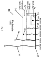
- Fig. 1 shows how the light penetration depths relate to a typical CMOS image sensor cross section.
- Efficient collection of the photogenerated electrons requires that the collection mechanism is located at or close to the penetration depth.
- the collection is assisted by the electric field produced by a PN junction.
- the junction is not located at an appropriate depth, i.e. a depth at or around the penetration depth of radiation to be detected, some the photogenerated electrons will diffuse to the junction, however a significant proportion will recombine and the signal will be lost.
- the quantum efficiency of a sensor having a junction at an inappropriate depth is 20%-30%, whereas the quantum efficiency of a sensor having a junction at an appropriate depth can be as high as 80%.
- the appropriate depth of P-N junction was guaranteed in an IR image sensor by either growing an epitaxial layer on a substrate to the thickness necessary to achieve a junction at the appropriate depth or by implanting a well structure deep enough to achieve a junction at the appropriate depth.
- both of these techniques significantly increase the fabrication time leading to increased cost.
- the depth of the Epitaxial layer / implant is usually 3pm - 5 ⁇ m. Increasing this depth will change the performance of the transistors requiring the models for the process to be re-extracted, which would be a time consuming and expensive process.
- CMOS image sensor arranged to comprise a radiation incident surface on the reverse surface thereof.
- An obverse surface of the CMOS image sensor is defined as the surface which is subject to steps of ion implantation to form active element and photodiode wells therein, and optionally to have pixel sensing circuitry fabricated thereupon.
- the reverse surface is defined as the surface opposed to the obverse surface, and can also be known as the "rear" or "back” surface.
- a radiation incident surface is defined as a surface upon which radiation impinges.
- the radiation incident surface comprises a thinned substrate layer.
- a thinned substrate layer we mean a substrate layer, for example a wafer, that has been thinned to have a thickness that is less than the thickness normally found for standard front-illuminated CMOS image sensors.
- the thinning can be carried out by any suitable process, most preferably by backlapping. There are two known types of thinning processes - mechanical grinding and chemical etching. Mechanical grinding is a quick method of removing silicon, but adds stress to the final wafer which can affect the performance, e.g. higher "dark current" (diode leakage) in a photosensor. Chemical etching avoids this stress, but is a very slow and therefore expensive process.
- Backlapping is commonly achieved by a mechanical grinding process where hundreds of microns of silicon are removed followed by a wet-etch process where a few microns to tens of microns are removed. This combines the speed of mechanical grinding but avoids the stress inducing part.
- the thinned substrate layer has a thickness approximately equal to the sum of a radiation absorption depth and a radiation collection junction depth.
- the radiation absorption depth is the depth, as measured from the radiation incident surface, that the incident radiation will penetrate before being absorbed, and hence lost to detection.
- the radiation collection junction depth is the depth as measured from the obverse surface of the CMOS image sensor, at which the P-N junction is formed.
- the thinned portion has a thickness that results in infra-red radiation being absorbed at or around the depth of the collection junction.
- the thinned portion can be any thickness within a range of thicknesses that may correspond to a successful absorption of radiation with a range of wavelengths in the infra-red region.
- the absorption of the radiation does not have to be exactly at the precise depth of the collection (P-N) junction, and so a thickness can be chosen that will give an optimised absorption for a specific desired wavelength of radiation, but also an improved absorption of a range of wavelengths that comprises the specific desired wavelength.
- the absorption depth of radiation of a specific wavelength is a statistical value, that is, one would normally expect radiation of a specific wavelength to be absorbed at a range of absorption depths, the range being well represented by the given figure for absorption depth.
- the concept of being absorbed "at" a particular depth therefore includes some minor variations around that depth for specific incoming radiation beams.
- the thinned portion has a thickness of between thirty and forty micrometers.
- a method of forming a CMOS image sensor comprising the step of arranging the sensor to comprise a radiation incident surface on the reverse surface thereof.
- the method comprises the step of thinning a substrate layer of the radiation incident surface.
- the step of thinning a substrate layer of the radiation incident surface comprises forming the substrate layer to have a thickness approximately equal to the sum of a radiation absorption depth and a radiation collection junction depth.
- the thinned portion has a thickness that results in infra-red radiation being absorbed at or around the depth of the collection junction.
- the thinned portion has a thickness of between thirty and forty micrometers.
- a method of sensing an image comprising the step of causing radiation to be incident on a reverse surface of a CMOS image sensor.
- CMOS photo sensor collects the photo generated charge in an implanted well and does not require the surface electrode.
- Fig. 1 shows selected components of a typical CMOS image sensor, including a P+ active element 10, an N-well 12, a P-epitaxial layer 14 and a P type substrate 16.
- Illustrated incident photons 18, 20, 22, 24 and 26 have wavelengths 450, 550, 650, 750 and 850 nm respectively.
- a typical P+ well 10 will have a depth of between about 0.5 ⁇ m to about 1.0 ⁇ m as measured from the light incident surface 28, while a typical N-well 12 will have a depth of about 2 ⁇ m to about 3 ⁇ m.
- the P-epitaxial layer 14 will have a depth of about 4 ⁇ m to about 5 ⁇ m, and the P substrate has a depth of 1mm, i.e. 1000 ⁇ m.
- the border between the N-well 12 and the P-epitaxial layer 14 defines a P-N junction 30.
- the penetration depth of photons with longer wavelength, i.e photons 22, 24 and 26 is greater than the depth of a standard silicon PN junction 30.
- the processed silicon wafer is thinned, for example using a backlapping process.
- the substrate 32 is thinned to a thickness of merely about 35 ⁇ m. This is a drastic reduction in size when compared to the 1mm depth of the substrate 16 of the image sensor of Fig. 1.
- Wafer thickness Optical Absorption Depth + Collection Junction Depth .
- the optimal wafer thickness is 33 ⁇ m.
- the invention improves IR response without the need for implanting a deeper junction.
- the device As the device is illuminated from the reverse side, it needs to be packaged in a suitable manner. For example, bump-bonded to a substrate with conductors, mounted on a lead-frame which has a hole allowing light to pass.
- ShellCase packaging technique glues a glass substrate to both the front and rear surfaces of the wafer: US 6,040,235 Badehi " Methods and apparatus for producing integrated circuit devices”.
- Thin wafers are particularly fragile, so it is usual for the thinning process to be carried out near the packaging factory. This minimizes damage to the wafer during transport.
- a wafer-scale packaging technique could be particularly advantageous. This would allow a support substrate to be bonded to the front-side of a wafer before it was thinned, adding mechanical support and strengthening the assembly. Once the support is in place, the silicon wafer could be thinned without it becoming fragile.
- An image sensor constructed in this way may be suitable for a number of applications including an optical mouse, an IR sensitive digital camera, or an IR communications device.
- the skilled man will readily appreciate the steps that are required to incorporate the image sensor of the invention into any of these products.
Landscapes
- Solid State Image Pick-Up Elements (AREA)
Abstract
A CMOS image sensor is provided, being arranged to comprise a radiation incident surface on the reverse surface thereof. The radiation radiation incident surface of the CMOS can comprise a thinned substrate layer, such that the CMOS image sensor improves infra-red response without the need for implanting deeper radiation collection junctions.
Description
- The present invention relates to a CMOS image sensor, in particular to improvements in the structure and function of a CMOS image sensor.
- Electromagnetic radiation in the infra-red spectrum has a longer wavelength than that in the visible spectrum, which produces a much longer penetration depth in silicon. For example, infra-red light having a wavelength of around 850nm, which is a common wavelength for communications applications, has a penetration depth of around 30µm in silicon.
- The relationship between incident wavelength and light penetration depth in a given material defines the material's optical absorption coefficient. Selected other values, as discussed in Sze "Physics of Semiconductor Devices" 2nd Edition, Chapter 13 "Photodetectors", are shown in the following table:
Wavelength Light Penetration Depth (µm) 450 0.5 550 2 650 5 750 10 850 30 - Fig. 1 shows how the light penetration depths relate to a typical CMOS image sensor cross section.
- Efficient collection of the photogenerated electrons requires that the collection mechanism is located at or close to the penetration depth. The collection is assisted by the electric field produced by a PN junction.
- If the junction is not located at an appropriate depth, i.e. a depth at or around the penetration depth of radiation to be detected, some the photogenerated electrons will diffuse to the junction, however a significant proportion will recombine and the signal will be lost. Typically, the quantum efficiency of a sensor having a junction at an inappropriate depth is 20%-30%, whereas the quantum efficiency of a sensor having a junction at an appropriate depth can be as high as 80%.
- Previously, the appropriate depth of P-N junction was guaranteed in an IR image sensor by either growing an epitaxial layer on a substrate to the thickness necessary to achieve a junction at the appropriate depth or by implanting a well structure deep enough to achieve a junction at the appropriate depth. However, both of these techniques significantly increase the fabrication time leading to increased cost.
- Furthermore, in a typical CMOS process, the depth of the Epitaxial layer / implant is usually 3pm - 5µm. Increasing this depth will change the performance of the transistors requiring the models for the process to be re-extracted, which would be a time consuming and expensive process.
- It is therefore desirable to provide an image sensor sensitive to infra-red radiation that can use standard CMOS processing technologies, but still maintain a reasonable quantum efficiency.
- According to a first aspect of the present invention, there is provided a CMOS image sensor arranged to comprise a radiation incident surface on the reverse surface thereof.
- An obverse surface of the CMOS image sensor is defined as the surface which is subject to steps of ion implantation to form active element and photodiode wells therein, and optionally to have pixel sensing circuitry fabricated thereupon. The reverse surface is defined as the surface opposed to the obverse surface, and can also be known as the "rear" or "back" surface. A radiation incident surface is defined as a surface upon which radiation impinges.
- Preferably, the radiation incident surface comprises a thinned substrate layer.
- By a thinned substrate layer, we mean a substrate layer, for example a wafer, that has been thinned to have a thickness that is less than the thickness normally found for standard front-illuminated CMOS image sensors. The thinning can be carried out by any suitable process, most preferably by backlapping. There are two known types of thinning processes - mechanical grinding and chemical etching. Mechanical grinding is a quick method of removing silicon, but adds stress to the final wafer which can affect the performance, e.g. higher "dark current" (diode leakage) in a photosensor. Chemical etching avoids this stress, but is a very slow and therefore expensive process. Backlapping is commonly achieved by a mechanical grinding process where hundreds of microns of silicon are removed followed by a wet-etch process where a few microns to tens of microns are removed. This combines the speed of mechanical grinding but avoids the stress inducing part.
- Preferably, the thinned substrate layer has a thickness approximately equal to the sum of a radiation absorption depth and a radiation collection junction depth.
- The radiation absorption depth is the depth, as measured from the radiation incident surface, that the incident radiation will penetrate before being absorbed, and hence lost to detection. The radiation collection junction depth is the depth as measured from the obverse surface of the CMOS image sensor, at which the P-N junction is formed.
- Preferably, the thinned portion has a thickness that results in infra-red radiation being absorbed at or around the depth of the collection junction.
- This means that the thinned portion can be any thickness within a range of thicknesses that may correspond to a successful absorption of radiation with a range of wavelengths in the infra-red region. The absorption of the radiation does not have to be exactly at the precise depth of the collection (P-N) junction, and so a thickness can be chosen that will give an optimised absorption for a specific desired wavelength of radiation, but also an improved absorption of a range of wavelengths that comprises the specific desired wavelength.
- It will also be appreciated that the absorption depth of radiation of a specific wavelength is a statistical value, that is, one would normally expect radiation of a specific wavelength to be absorbed at a range of absorption depths, the range being well represented by the given figure for absorption depth. The concept of being absorbed "at" a particular depth therefore includes some minor variations around that depth for specific incoming radiation beams.
- Preferably, the thinned portion has a thickness of between thirty and forty micrometers.
- According to a second aspect of the invention, there is provided a method of forming a CMOS image sensor, comprising the step of arranging the sensor to comprise a radiation incident surface on the reverse surface thereof.
- Preferably, the method comprises the step of thinning a substrate layer of the radiation incident surface.
- Preferably, the step of thinning a substrate layer of the radiation incident surface comprises forming the substrate layer to have a thickness approximately equal to the sum of a radiation absorption depth and a radiation collection junction depth.
- Preferably, the thinned portion has a thickness that results in infra-red radiation being absorbed at or around the depth of the collection junction.
- Preferably, the thinned portion has a thickness of between thirty and forty micrometers.
- According to a third aspect of the invention, there is provided a method of sensing an image, comprising the step of causing radiation to be incident on a reverse surface of a CMOS image sensor.
- The present invention will now be described, by way of example only, with reference to the accompanying drawings, in which:
- Fig. 1 shows a prior art image sensor and illustrates the light penetration depth of incident radiation; and
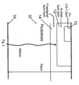
- Fig. 2 shows an image sensor in accordance with a first embodiment of the invention.
- Backside illumination of image sensors incorporating charge coupled devices (CCDs) is well known, as it has been desirable to overcome the poor optical transmission properties of the front-side control electrodes. An example of a back-illuminated CCD image sensor can be seen in US 4,266,334, to Edwards et. al.
- However, it has not previously been known to have backside illumination of CMOS image sensors. The electrodes of a CCD are required to generate an alternating series of "potential wells" in which the photo-electric generated charge is first collected and then transported around the device. This technique led to the name "Charge Coupled Device". The noise-free charge-transfer technique of a CCD partially mitigates against the reduction in photosensitivity caused by the optical absorbtion of the front electrodes.
- In contrast to this technique, a CMOS photo sensor collects the photo generated charge in an implanted well and does not require the surface electrode. As a result of this more light-efficient sturcture, there is neither a requirement or a benefit of having back-illuminated CMOS device for traditional operation.
- Fig. 1 shows selected components of a typical CMOS image sensor, including a P+
active element 10, an N-well 12, a P-epitaxial layer 14 and aP type substrate 16. Illustratedincident photons - As indicated in Fig. 1, a
typical P+ well 10 will have a depth of between about 0.5 µm to about 1.0 µm as measured from thelight incident surface 28, while a typical N-well 12 will have a depth of about 2 µm to about 3 µm. The P-epitaxial layer 14 will have a depth of about 4 µm to about 5 µm, and the P substrate has a depth of 1mm, i.e. 1000 µm. - The border between the N-
well 12 and the P-epitaxial layer 14 defines a P-N junction 30. As can be seen from Figure 1, the penetration depth of photons with longer wavelength, i.ephotons - Selected components of a CMOS image sensor according to a preferred embodiment are illustrated in Figure 2. Like components are labelled with like reference numerals.
- To make the CMOS image sensor of figure 2, the processed silicon wafer is thinned, for example using a backlapping process. The
substrate 32 is thinned to a thickness of merely about 35 µm. This is a drastic reduction in size when compared to the 1mm depth of thesubstrate 16 of the image sensor of Fig. 1. - There is of course a general overriding desire to manufacture sensors that are small in size, but a reduction of thickness of this magnitude has not previously been considered due to the greatly increased fragility of such a wafer, which would be seen to result in an undesirable wastage due to breakage. However, the inventor has realised that such a thinned wafer can be useful to construct an improved IR sensor, thus providing an advantageous effect to counteract any problems with the wafer's fragility.
- The sensor is then illuminated from the reverse side, via
light incident surface 34. The wafer thinning can be optimized for the illumination:
- For the case of a sensor with an Nwell / Pepitaxial collection with junction depth of 3µm and 850nm wavelength illumination (and hence penetration depth of 30µm), the optimal wafer thickness is 33µm.
- Thus, the invention improves IR response without the need for implanting a deeper junction.
- As the device is illuminated from the reverse side, it needs to be packaged in a suitable manner. For example, bump-bonded to a substrate with conductors, mounted on a lead-frame which has a hole allowing light to pass.
- Various packaging technologies are particularly suitable for this technique. For example the ShellCase packaging technique, glues a glass substrate to both the front and rear surfaces of the wafer: US 6,040,235 Badehi " Methods and apparatus for producing integrated circuit devices".
- Thin wafers are particularly fragile, so it is usual for the thinning process to be carried out near the packaging factory. This minimizes damage to the wafer during transport. Alternatively, a wafer-scale packaging technique could be particularly advantageous. This would allow a support substrate to be bonded to the front-side of a wafer before it was thinned, adding mechanical support and strengthening the assembly. Once the support is in place, the silicon wafer could be thinned without it becoming fragile.
- An image sensor constructed in this way may be suitable for a number of applications including an optical mouse, an IR sensitive digital camera, or an IR communications device. The skilled man will readily appreciate the steps that are required to incorporate the image sensor of the invention into any of these products.
- Various improvements and modifications can be made to the above without departing from the scope of the invention. In particular, the skilled man will realise the doping types of the specific embodiment illustrated may straightforwardly be switched.
Claims (14)
- A CMOS image sensor arranged to comprise a radiation incident surface on the reverse surface thereof.
- The CMOS image sensor of claim 1, wherein the radiation incident surface comprises a thinned substrate layer.
- The CMOS image sensor of claim 2, wherein the thinned substrate layer has a thickness approximately equal to the sum of a radiation absorption depth and a radiation collection junctio depth.
- The CMOS image sensor of claim 3, wherein the thinned portion has a thickness that results in infra-red radiation being absorbed at or around the depth of the collection junction.
- The CMOS image sensor of claim 2 or claim 3, wherein the thinned portion has a thickness of between twenty and forty micrometers.
- An optical mouse comprising the CMOS image sensor of any preceding claim.
- An IR sensitive digital camera comprising the CMOS image sensor of any of claims 1-5.
- A communications device comprising the CMOS image sensor of any of claims 1-5.
- A method of forming a CMOS image sensor, comprising the step of arranging the sensor to comprise a radiation incident surface on the reverse surface thereof.
- The method of claim 9, comprising the step of thinning a substrate layer of the radiation incident surface.
- The method of claim 10, wherein the step of thinning a substrate layer of the radiation incident surface comprises forming the substrate layer to have a thickness approximately equal to the sum of a radiation absorption depth and a radiation collection junction depth.
- The method of claim 11, wherein the thinned portion has a thickness that results in infra-red radiation being absorbed at or around the depth of the collection junction.
- The method of claim 11 or claim 12, wherein the thinned portion has a thickness of between thirty and forty micrometers.
- A method of sensing an image, comprising the step of causing radiation to be incident on a reverse surface of a CMOS image sensor.
Priority Applications (1)
| Application Number | Priority Date | Filing Date | Title |
|---|---|---|---|
| EP04257208A EP1659630A1 (en) | 2004-11-18 | 2004-11-18 | CMOS image sensor |
Applications Claiming Priority (1)
| Application Number | Priority Date | Filing Date | Title |
|---|---|---|---|
| EP04257208A EP1659630A1 (en) | 2004-11-18 | 2004-11-18 | CMOS image sensor |
Publications (1)
| Publication Number | Publication Date |
|---|---|
| EP1659630A1 true EP1659630A1 (en) | 2006-05-24 |
Family
ID=34930816
Family Applications (1)
| Application Number | Title | Priority Date | Filing Date |
|---|---|---|---|
| EP04257208A Withdrawn EP1659630A1 (en) | 2004-11-18 | 2004-11-18 | CMOS image sensor |
Country Status (1)
| Country | Link |
|---|---|
| EP (1) | EP1659630A1 (en) |
Citations (4)
| Publication number | Priority date | Publication date | Assignee | Title |
|---|---|---|---|---|
| US6169319B1 (en) * | 1999-08-12 | 2001-01-02 | Tower Semiconductor Ltd. | Backside illuminated image sensor |
| US20010017344A1 (en) * | 1999-07-20 | 2001-08-30 | Aebi Verle W. | Electron bombarded passive pixel sensor imaging |
| US20040005729A1 (en) * | 2002-03-19 | 2004-01-08 | Takashi Abe | Solid state image pickup device and method of producing solid state image pickup device |
| WO2004070785A2 (en) * | 2003-01-31 | 2004-08-19 | Intevac, Inc. | Backside thinning of image array devices |
-
2004
- 2004-11-18 EP EP04257208A patent/EP1659630A1/en not_active Withdrawn
Patent Citations (4)
| Publication number | Priority date | Publication date | Assignee | Title |
|---|---|---|---|---|
| US20010017344A1 (en) * | 1999-07-20 | 2001-08-30 | Aebi Verle W. | Electron bombarded passive pixel sensor imaging |
| US6169319B1 (en) * | 1999-08-12 | 2001-01-02 | Tower Semiconductor Ltd. | Backside illuminated image sensor |
| US20040005729A1 (en) * | 2002-03-19 | 2004-01-08 | Takashi Abe | Solid state image pickup device and method of producing solid state image pickup device |
| WO2004070785A2 (en) * | 2003-01-31 | 2004-08-19 | Intevac, Inc. | Backside thinning of image array devices |
Similar Documents
| Publication | Publication Date | Title |
|---|---|---|
| US6498336B1 (en) | Integrated light sensors with back reflectors for increased quantum efficiency | |
| US8946818B2 (en) | Dark current reduction in back-illuminated imaging sensors | |
| TWI300987B (en) | Solid-state image pickup device | |
| US8048711B2 (en) | Method for forming deep isolation in imagers | |
| US7985612B2 (en) | Method and device for reducing crosstalk in back illuminated imagers | |
| CN111937151B (en) | Photodetector | |
| US20070052050A1 (en) | Backside thinned image sensor with integrated lens stack | |
| EP2267795A2 (en) | Avalanche photodiode | |
| EP0917206A1 (en) | CMOS image sensor | |
| US20080070340A1 (en) | Image sensor using thin-film SOI | |
| KR20110038133A (en) | Backlit image sensor with reduced dark current | |
| CN102630343B (en) | Solid-state image pickup device and manufacturing method thereof | |
| US20080296475A1 (en) | Vertical image sensors and methods of fabricating the same | |
| US20130001729A1 (en) | High Fill-Factor Laser-Treated Semiconductor Device on Bulk Material with Single Side Contact Scheme | |
| Jerram et al. | Back-thinned CMOS sensor optimization | |
| US9520441B2 (en) | Method for electronically pinning a back surface of a back-illuminated imager fabricated on a UTSOI wafer | |
| JP5600690B2 (en) | Avalanche photodiode and manufacturing method thereof | |
| US8053853B2 (en) | Color filter-embedded MSM image sensor | |
| US7982277B2 (en) | High-efficiency thinned imager with reduced boron updiffusion | |
| US11374040B1 (en) | Pixel arrays including heterogenous photodiode types | |
| EP1453100B1 (en) | Image sensing structure | |
| US7504277B2 (en) | Method for fabricating a high performance PIN focal plane structure using three handle wafers | |
| WO2006043105A1 (en) | Electro-optical device | |
| Hinckley et al. | Modelling of device structure effects in backside illuminated CMOS compatible photodiodes |
Legal Events
| Date | Code | Title | Description |
|---|---|---|---|
| PUAI | Public reference made under article 153(3) epc to a published international application that has entered the european phase |
Free format text: ORIGINAL CODE: 0009012 |
|
| AK | Designated contracting states |
Kind code of ref document: A1 Designated state(s): AT BE BG CH CY CZ DE DK EE ES FI FR GB GR HU IE IS IT LI LU MC NL PL PT RO SE SI SK TR |
|
| AX | Request for extension of the european patent |
Extension state: AL HR LT LV MK YU |
|
| AKX | Designation fees paid | ||
| REG | Reference to a national code |
Ref country code: DE Ref legal event code: 8566 |
|
| STAA | Information on the status of an ep patent application or granted ep patent |
Free format text: STATUS: THE APPLICATION IS DEEMED TO BE WITHDRAWN |
|
| 18D | Application deemed to be withdrawn |
Effective date: 20061127 |