EP1655780A2 - Image sensor and pixel having an anti-reflective coating over the photodiode - Google Patents
Image sensor and pixel having an anti-reflective coating over the photodiode Download PDFInfo
- Publication number
- EP1655780A2 EP1655780A2 EP05256688A EP05256688A EP1655780A2 EP 1655780 A2 EP1655780 A2 EP 1655780A2 EP 05256688 A EP05256688 A EP 05256688A EP 05256688 A EP05256688 A EP 05256688A EP 1655780 A2 EP1655780 A2 EP 1655780A2
- Authority
- EP
- European Patent Office
- Prior art keywords
- pixel
- photodiode
- reflective coating
- sio
- image sensor
- Prior art date
- Legal status (The legal status is an assumption and is not a legal conclusion. Google has not performed a legal analysis and makes no representation as to the accuracy of the status listed.)
- Granted
Links
Images

Classifications
-
- H—ELECTRICITY
- H10—SEMICONDUCTOR DEVICES; ELECTRIC SOLID-STATE DEVICES NOT OTHERWISE PROVIDED FOR
- H10F—INORGANIC SEMICONDUCTOR DEVICES SENSITIVE TO INFRARED RADIATION, LIGHT, ELECTROMAGNETIC RADIATION OF SHORTER WAVELENGTH OR CORPUSCULAR RADIATION
- H10F39/00—Integrated devices, or assemblies of multiple devices, comprising at least one element covered by group H10F30/00, e.g. radiation detectors comprising photodiode arrays
- H10F39/80—Constructional details of image sensors
- H10F39/805—Coatings
-
- H—ELECTRICITY
- H10—SEMICONDUCTOR DEVICES; ELECTRIC SOLID-STATE DEVICES NOT OTHERWISE PROVIDED FOR
- H10F—INORGANIC SEMICONDUCTOR DEVICES SENSITIVE TO INFRARED RADIATION, LIGHT, ELECTROMAGNETIC RADIATION OF SHORTER WAVELENGTH OR CORPUSCULAR RADIATION
- H10F39/00—Integrated devices, or assemblies of multiple devices, comprising at least one element covered by group H10F30/00, e.g. radiation detectors comprising photodiode arrays
- H10F39/011—Manufacture or treatment of image sensors covered by group H10F39/12
- H10F39/024—Manufacture or treatment of image sensors covered by group H10F39/12 of coatings or optical elements
-
- H—ELECTRICITY
- H10—SEMICONDUCTOR DEVICES; ELECTRIC SOLID-STATE DEVICES NOT OTHERWISE PROVIDED FOR
- H10F—INORGANIC SEMICONDUCTOR DEVICES SENSITIVE TO INFRARED RADIATION, LIGHT, ELECTROMAGNETIC RADIATION OF SHORTER WAVELENGTH OR CORPUSCULAR RADIATION
- H10F39/00—Integrated devices, or assemblies of multiple devices, comprising at least one element covered by group H10F30/00, e.g. radiation detectors comprising photodiode arrays
- H10F39/10—Integrated devices
- H10F39/12—Image sensors
- H10F39/18—Complementary metal-oxide-semiconductor [CMOS] image sensors; Photodiode array image sensors
-
- H—ELECTRICITY
- H10—SEMICONDUCTOR DEVICES; ELECTRIC SOLID-STATE DEVICES NOT OTHERWISE PROVIDED FOR
- H10F—INORGANIC SEMICONDUCTOR DEVICES SENSITIVE TO INFRARED RADIATION, LIGHT, ELECTROMAGNETIC RADIATION OF SHORTER WAVELENGTH OR CORPUSCULAR RADIATION
- H10F39/00—Integrated devices, or assemblies of multiple devices, comprising at least one element covered by group H10F30/00, e.g. radiation detectors comprising photodiode arrays
- H10F39/80—Constructional details of image sensors
- H10F39/803—Pixels having integrated switching, control, storage or amplification elements
Definitions
- the present invention relates to image sensors, and more particularly, to an image sensor that uses pixels having an anti-reflective coating atop of the photodiode.
- Image sensors have become ubiquitous. They are widely used in digital still cameras, cellular phones, security cameras, medical, automobile, and other applications.
- the technology used to manufacture image sensors, and in particular CMOS image sensors, has continued to advance at great pace. For example, the demands of higher resolution and lower power consumption have encouraged the further miniaturization and integration of the image sensor.
- the pixel typically has a light-sensing element, such as a photodiode, which receives incident light and produces a signal in relation to the amount of incident light. Because of the small size of the light-sensing element, it is important that as much incident light is captured by the light-sensing element.
- a light-sensing element such as a photodiode
- One major source of incident light loss occurs as a result of reflection at the photodiode (the silicon surface) to oxide (SiO 2 ) interface. At this interface, a substantial amount of light is reflected with the consequential reduction in photodiode responsivity and quantum efficiency.
- the present invention provides a pixel according to Claim 1 or Claim 20 and an image sensor according to Claim 35.
- Figure 1 shows a combination cross-sectional and schematic view of an active pixel that uses four transistors. This is known in the art as a 4T active pixel.
- a light-sensing element in this embodiment a photodiode 101, outputs a signal that is used to modulate an amplification transistor 103.
- the amplification transistor 103 is also referred to as a source follower transistor. While the light-sensing element can be one of a variety of devices, including without limitation, photogates, photodiodes, pinned photodiodes, partially pinned photodiodes, etc., in the present invention, the light-sensing element is a photodiode (whether of the pinned, partially pinned, or unpinned variety).
- a transfer transistor 105 is used to transfer the signal output by the photodiode 101 to a floating node 107, which is connected to the gate of the amplification transistor 105. The transfer transistor 105 is controlled by a transfer gate.
- a characteristic feature of a 4T active pixel is the presence of a transfer gate to enable true correlated double sampling (CDS). It is possible to eliminate the row select (RS) transistor in the 4T pixel to form a "4T active pixel" with just three transistors by additionally gating the supply voltage to the reset transistors. It is to be understood that this invention applies to all CMOS imagers whether they be formed with 3, 4, 5, 6, or more transistors. This invention also applies to CCD image sensors.
- the photodiode 101 In operation, during an integration period (also referred to as an exposure or accumulation period), the photodiode 101 generates charge that is held in the N-type layer. After the integration period, the transfer transistor 105 is turned on to transfer the charge held in the N-type layer of the photodiode 101 to the floating node 107. After the signal has been transferred to the floating node 107, the transfer transistor 105 is turned off again for the start of a subsequent integration period.
- the signal on the floating node 107 is then used to modulate the amplification transistor 105.
- an address transistor 109 is used as a means to address the pixel and to selectively read out the signal onto a column bit line 111.
- a reset transistor 113 resets the floating node 107 to a reference voltage.
- the reference voltage is V dd . Note that while the description herein discusses the present invention in the context of a 4T pixel, the present invention may be used with a 3T, 5T, 6T, 7T or other pixel designs. In fact, the use of the present invention may be applied to any light sensing element or with either CMOS or CCD image sensors.
- Figure 1A shows a three transistor (3T) pixel design.
- the transfer transistor is omitted and the output node of the photodiode is directly connected to the amplification transistor 103.
- the reset transistor 113 is adjacent the photodiode 101 and can selectively reset the output of the photodiode to the reference voltage V dd .
- incident light 115 is incident onto the photodiode 101. However, some portion of the incident light 115 is reflected as reflected light 117. This reflected light 117 is "wasted", i.e. not sensed by the photodiode 101.
- the present invention reduces the reflection from the surface of the photodiode 101 by adding an anti-reflective coating (ARC).
- ARC anti-reflective coating
- the inclusion of an anti-reflective coating over the light sensing element (the photodiode) 101 substantially reduces the loss of incident light due to reflection. Note that while the description herein shows the application of the present invention with respect to CMOS pixels, the present invention can be equally applied to CCD pixels.
- the anti-reflective coating is placed close to the silicon surface and over the photodiode 101.
- the photodiode ARC should be transparent to light in the visible spectrum and have an index of refraction between that of the overlying oxide and the underlying silicon substrate (the photodiode region).
- the ARC is silicon nitride (Si 3 N 4 ). It should be noted that other types of anti-reflective coatings may also be suitable, such as those commercially available from Brewer Science of Rolla, MO. Thus, that the use of silicon nitride is but one example of a suitable anti-reflective coating.
- the ARC may be silicon oxynitride (SiO x N y ) or a multilayer stack, such as SiO 2 /Si 3 N 4 , SiO x N y /Si 3 N 4 , or SiO x N y /Si 3 N 4 /SiO w N z .
- a graded stack such as SiO x N y /Si 3 O c N w /SiO q /N u may be used.
- the thickness of the silicon nitride anti-reflective coating layer should be chosen to be appropriate to eliminate reflections near the incident wavelengths that are being detected.
- the thickness of the silicon nitride layer may be approximately 550 Angstroms.
- T OPT the optimum nitride thickness
- the thickness T OPT is approximately 535 Angstroms.
- the spectrum of incident light varies approximately between 4000 to 7000 angstroms
- This photodiode ARC could be a multilayer stack such as SiO x N y /Si 3 N 4 or a material with a graded index of refraction.
- a material with a graded index of refraction can be formed by varying the flow of oxygen and nitrogen during the SiO x N y deposition. This may result in the range of thickness of the ARC to be between 200 to 1500 angstroms, and perhaps in the narrower range of 300-1000 angstroms.
- silicon nitride ARC is placed in direct contact with the silicon substrate, this will likely cause an increase in interface state density at the photodiode surface that may cause an increase in photodiode dark current.
- silicon nitride in contact with silicon is also known to result in stress to the underlying silicon. Therefore, in one embodiment, the silicon nitride anti-reflective coating is separated from the photodiode silicon surface.
- the present invention is intended to cover the broad concept of using an anti-reflective coating formed atop of a light-sensing element, such as a photodiode.
- a light-sensing element such as a photodiode.
- the described embodiment herein teaches the use of a silicon nitride anti-reflective coating atop of the photodiode silicon surface and separated by some type of buffering layer, the present invention should not be construed more broadly to eliminate the buffer layer.
- a thin oxide such as silicon oxide
- the silicon nitride anti-reflective coating can be deposited.
- Figures 2-4 one method for forming the anti-reflective coating is shown. Specifically, as seen in Figure 2, a cross-section view of two adjacent pixels is shown. Two pixels are shown to more accurately reflect the layout of an actual image sensor.
- photodiodes 101 are formed adjacent to each other in a semiconductor substrate 201.
- the two pixels 101 are separated by a field oxide, in this example, a shallow trench isolation (STI).
- STI shallow trench isolation
- the photodiodes shown in Figures 2-4 are pinned photodiodes.
- the transfer transistor that has its transfer gate controlled by a signal TG.
- a reset transistor is formed adjacent to the transfer transistor. The gate of the reset transistor is controlled by the signal RST.
- Figure 2 shows an intermediate structure in the formation of an image sensor.
- the photodiodes 101 have been formed in the substrate 201 and the P+ pinning layers have also been formed.
- the gates of the transfer transistors and the reset transistors have also been formed atop of a gate oxide.
- the polysilicon that forms the gates of the transfer and reset transistors are shown in crosshatch.
- a thin oxide is either thermally grown, such as by thermal oxidation of the polysilicon and silicon substrate.
- the thin oxide 203 alternatively, may be formed by deposition, such as by a chemical vapor deposition or a plasma-enhanced chemical vapor deposition process.
- the thin oxide 203 is between 20 and 100 angstroms.
- One purpose of the thin oxide 203 is to grow a locally thick oxide at the edge of the polysilicon gates which locally thickens the gate oxide, thereby reduces the electric field at the transistor gate edge, and therefore improves the transistor reliability to high electron degradation.
- an anti-reflective coating such as silicon nitride
- the anti-reflective coating 301 is then patterned and etched so that the anti-reflective coating covers substantially only the photodiode regions 101.
- the anti-reflective coating is removed from non-photodiode regions of the image sensor. This may be important because the anti-reflective coating, in the case of silicon nitride, acts as a barrier to hydrogen penetration during alloying steps. If the silicon nitride were to remain, then beneficial hydrogen annealing that reduces silicon/gate oxide surface state density would be blocked.
- sidewall spacers are formed on the exposed sidewalls of the transfer gate and the gate of the reset transistor.
- the sidewall spacers may be formed by deposition of an oxide followed by an etching back process.
- the N + regions 401 and 403 are formed in the substrate using implantation techniques.
- a planarization layer such as a planar oxide 405 is formed over the entire pixel.
- an anti-reflective layer can be formed between the planar oxide layer 405 and the underlying photodiode 101.
- a thin oxide is used as a buffer or stress-relieving layer between the anti-reflective coating 301 and the silicon surface.
- the thin oxide layer may not be absolutely necessary.
- the use of the anti-reflective coating 301 substantially reduces the amount of reflection of incident light onto the photodiode 101. This causes increased incident light to actually reach the photodiode and therefore generate greater signal.
- Figures 5 and 6 illustrate an alternative method for forming the anti-reflective coating. Specifically, as seen in Figure 5, after the transfer gates and the reset gates are formed, sidewall spacers are formed on the gates, such as by a blanket deposition of oxide followed by an etchback. Next, typically the N + regions 401 and 403 are formed in the substrate 203 by ion implantation. Note that the N + region 401 is the floating node and the N-plus region 403 is typically connected to V DD . Next, a thin oxide layer 203 is formed over the exposed polysilicon and the exposed silicon substrate.
- the anti-reflective coating layer 301 is formed over the pixels and patterned such that it is only covering the photodiodes 101.
- a silicon nitride layer is used as the anti-reflection coating.
- a multilayer ARC [SiO x N y /Si 3 N 4 /SiO w N z ] or an ARC with a graded index of refraction such as SiO x N y /SiO c N w /SiO q /N u may be deposited.
Landscapes
- Solid State Image Pick-Up Elements (AREA)
- Transforming Light Signals Into Electric Signals (AREA)
Abstract
Description
- The present invention relates to image sensors, and more particularly, to an image sensor that uses pixels having an anti-reflective coating atop of the photodiode.
- Image sensors have become ubiquitous. They are widely used in digital still cameras, cellular phones, security cameras, medical, automobile, and other applications. The technology used to manufacture image sensors, and in particular CMOS image sensors, has continued to advance at great pace. For example, the demands of higher resolution and lower power consumption have encouraged the further miniaturization and integration of the image sensor.
- As the pixels become smaller, the surface area that can receive incident light is also reduced. The pixel typically has a light-sensing element, such as a photodiode, which receives incident light and produces a signal in relation to the amount of incident light. Because of the small size of the light-sensing element, it is important that as much incident light is captured by the light-sensing element. One major source of incident light loss occurs as a result of reflection at the photodiode (the silicon surface) to oxide (SiO2) interface. At this interface, a substantial amount of light is reflected with the consequential reduction in photodiode responsivity and quantum efficiency.
- According to various aspects, the present invention provides a pixel according to Claim 1 or Claim 20 and an image sensor according to Claim 35.
-
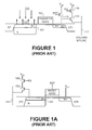
- Figure 1 is a combination cross-sectional and schematic diagram of a prior art four transistor (4T) pixel which shows in detail a photodiode formed in a substrate.
- Figure 1A is a combination cross-sectional and schematic diagram of a prior art three transistor (3T) pixel which shows in detail a photodiode formed in a substrate.
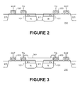
- Figures 2-4 are cross sectional views illustrating the process of manufacturing a pixel with an anti-reflective coating in accordance with the present invention.
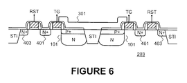
- Figures 5 and 6 are cross sectional views illustrating an alternative process for manufacturing an anti-reflective coating.
- In the following description, numerous specific details are provided in order to give a thorough understanding of embodiments of the invention. One skilled in the relevant art will recognize, however, that the invention may be practiced without one or more of the specific details, or with other methods, components, materials, etc. In other instances, well known structures, materials, or operations are not shown or described in order to avoid obscuring aspects of the invention.
- Referenced throughout the specification to "one embodiment" or "an embodiment" means that a particular feature, structure, or characteristic described in connection with the embodiment and included in at least one embodiment of the present invention. Thus, the appearances of the phrase "in one embodiment" or "in an embodiment" in various places throughout the specification are not necessarily all referring to the same embodiment. Furthermore, the particular features, structures, or characteristics may be combined in any suitable manner in one or more embodiments.
- Figure 1 shows a combination cross-sectional and schematic view of an active pixel that uses four transistors. This is known in the art as a 4T active pixel. A light-sensing element, in this embodiment a
photodiode 101, outputs a signal that is used to modulate anamplification transistor 103. Theamplification transistor 103 is also referred to as a source follower transistor. While the light-sensing element can be one of a variety of devices, including without limitation, photogates, photodiodes, pinned photodiodes, partially pinned photodiodes, etc., in the present invention, the light-sensing element is a photodiode (whether of the pinned, partially pinned, or unpinned variety). Atransfer transistor 105 is used to transfer the signal output by thephotodiode 101 to afloating node 107, which is connected to the gate of theamplification transistor 105. Thetransfer transistor 105 is controlled by a transfer gate. - A characteristic feature of a 4T active pixel is the presence of a transfer gate to enable true correlated double sampling (CDS). It is possible to eliminate the row select (RS) transistor in the 4T pixel to form a "4T active pixel" with just three transistors by additionally gating the supply voltage to the reset transistors. It is to be understood that this invention applies to all CMOS imagers whether they be formed with 3, 4, 5, 6, or more transistors. This invention also applies to CCD image sensors.
- In operation, during an integration period (also referred to as an exposure or accumulation period), the
photodiode 101 generates charge that is held in the N-type layer. After the integration period, thetransfer transistor 105 is turned on to transfer the charge held in the N-type layer of thephotodiode 101 to thefloating node 107. After the signal has been transferred to thefloating node 107, thetransfer transistor 105 is turned off again for the start of a subsequent integration period. - The signal on the
floating node 107 is then used to modulate theamplification transistor 105. Finally, anaddress transistor 109 is used as a means to address the pixel and to selectively read out the signal onto acolumn bit line 111. After readout through thecolumn bit line 111, areset transistor 113 resets thefloating node 107 to a reference voltage. In one embodiment, the reference voltage is Vdd. Note that while the description herein discusses the present invention in the context of a 4T pixel, the present invention may be used with a 3T, 5T, 6T, 7T or other pixel designs. In fact, the use of the present invention may be applied to any light sensing element or with either CMOS or CCD image sensors. - Figure 1A shows a three transistor (3T) pixel design. In this design, the transfer transistor is omitted and the output node of the photodiode is directly connected to the
amplification transistor 103. Further, thereset transistor 113 is adjacent thephotodiode 101 and can selectively reset the output of the photodiode to the reference voltage Vdd. - As can be seen in Figures 1 and 1A,
incident light 115 is incident onto thephotodiode 101. However, some portion of theincident light 115 is reflected as reflectedlight 117. Thisreflected light 117 is "wasted", i.e. not sensed by thephotodiode 101. - The present invention reduces the reflection from the surface of the
photodiode 101 by adding an anti-reflective coating (ARC). The inclusion of an anti-reflective coating over the light sensing element (the photodiode) 101 substantially reduces the loss of incident light due to reflection. Note that while the description herein shows the application of the present invention with respect to CMOS pixels, the present invention can be equally applied to CCD pixels. - In one embodiment, the anti-reflective coating is placed close to the silicon surface and over the
photodiode 101. In general, it has been found that the photodiode ARC should be transparent to light in the visible spectrum and have an index of refraction between that of the overlying oxide and the underlying silicon substrate (the photodiode region). In one embodiment, the ARC is silicon nitride (Si3N4). It should be noted that other types of anti-reflective coatings may also be suitable, such as those commercially available from Brewer Science of Rolla, MO. Thus, that the use of silicon nitride is but one example of a suitable anti-reflective coating. For example, the ARC may be silicon oxynitride (SiOxNy) or a multilayer stack, such as SiO2/Si3N4, SiOxNy/Si3N4, or SiOxNy/Si3N4/SiOwNz. Alternatively, a graded stack such as SiOxNy/Si3OcNw/SiOq/Nu may be used. - Furthermore, the thickness of the silicon nitride anti-reflective coating layer should be chosen to be appropriate to eliminate reflections near the incident wavelengths that are being detected. For an image sensor that is designed to be sensitive to visible radiation, the thickness of the silicon nitride layer may be approximately 550 Angstroms.
- Specifically, assume that the optimum nitride thickness is designated as TOPT· Then, the following formula is an approximation of the value of TOPT:

- If we assume that the index of refraction NNitride is approximately 2.1, then for an incident wavelength A of 4500 Angstroms (blue color), the thickness TOPT is approximately 535 Angstroms.
- In other embodiments, where the spectrum of incident light varies approximately between 4000 to 7000 angstroms, this gives a range of thickness for the anti-reflective coating formed of silicon nitride of between approximately between 470 angstroms and 830 angstroms. While a range has been give, it can be appreciated that the thickness of the silicon nitride may be less than or more than the range depending upon the specific application. The thickness for any given application will depend on the index of refraction of the photodiode ARC. This photodiode ARC could be a multilayer stack such as SiOxNy/Si3N4 or a material with a graded index of refraction. A material with a graded index of refraction can be formed by varying the flow of oxygen and nitrogen during the SiOxNy deposition. This may result in the range of thickness of the ARC to be between 200 to 1500 angstroms, and perhaps in the narrower range of 300-1000 angstroms.
- If the silicon nitride ARC is placed in direct contact with the silicon substrate, this will likely cause an increase in interface state density at the photodiode surface that may cause an increase in photodiode dark current. Furthermore, silicon nitride in contact with silicon is also known to result in stress to the underlying silicon. Therefore, in one embodiment, the silicon nitride anti-reflective coating is separated from the photodiode silicon surface. However, it can be appreciated in other embodiments, there may be other anti-reflective coatings that can be placed directly atop of the silicon surface without detrimental effect.
- The present invention is intended to cover the broad concept of using an anti-reflective coating formed atop of a light-sensing element, such as a photodiode. Thus, while the described embodiment herein teaches the use of a silicon nitride anti-reflective coating atop of the photodiode silicon surface and separated by some type of buffering layer, the present invention should not be construed more broadly to eliminate the buffer layer.
- In the embodiment described herein, a thin oxide, such as silicon oxide, is formed, such as by deposition or by thermal growth, over the photodiode silicon surface. After the thin oxide layer is formed, the silicon nitride anti-reflective coating can be deposited. Turning to Figures 2-4, one method for forming the anti-reflective coating is shown. Specifically, as seen in Figure 2, a cross-section view of two adjacent pixels is shown. Two pixels are shown to more accurately reflect the layout of an actual image sensor.
- As seen in Figure 2,
photodiodes 101 are formed adjacent to each other in asemiconductor substrate 201. The twopixels 101 are separated by a field oxide, in this example, a shallow trench isolation (STI). Further, the photodiodes shown in Figures 2-4 are pinned photodiodes. However, it can be appreciated that the present invention can be applied to any type of light-sensing element. Also shown in Figure 2 is the transfer transistor that has its transfer gate controlled by a signal TG. Moreover, a reset transistor is formed adjacent to the transfer transistor. The gate of the reset transistor is controlled by the signal RST. - Figure 2 shows an intermediate structure in the formation of an image sensor. In this intermediate structure, the
photodiodes 101 have been formed in thesubstrate 201 and the P+ pinning layers have also been formed. Furthermore, the gates of the transfer transistors and the reset transistors have also been formed atop of a gate oxide. The polysilicon that forms the gates of the transfer and reset transistors are shown in crosshatch. - At this point, in accordance with one embodiment of the present invention, a thin oxide is either thermally grown, such as by thermal oxidation of the polysilicon and silicon substrate. The
thin oxide 203, alternatively, may be formed by deposition, such as by a chemical vapor deposition or a plasma-enhanced chemical vapor deposition process. In one embodiment, thethin oxide 203 is between 20 and 100 angstroms. - One purpose of the
thin oxide 203 is to grow a locally thick oxide at the edge of the polysilicon gates which locally thickens the gate oxide, thereby reduces the electric field at the transistor gate edge, and therefore improves the transistor reliability to high electron degradation. - Turning next to Figure 3, an anti-reflective coating, such as silicon nitride, is then deposited or otherwise formed. The
anti-reflective coating 301 is then patterned and etched so that the anti-reflective coating covers substantially only thephotodiode regions 101. In this embodiment, the anti-reflective coating is removed from non-photodiode regions of the image sensor. This may be important because the anti-reflective coating, in the case of silicon nitride, acts as a barrier to hydrogen penetration during alloying steps. If the silicon nitride were to remain, then beneficial hydrogen annealing that reduces silicon/gate oxide surface state density would be blocked. - Again, if a different anti-reflective coating material is used that would allow hydrogen penetration, then it may not be necessary to remove the anti-reflective coating from the non-photodiode regions.
- Next, turning to Figure 4, sidewall spacers are formed on the exposed sidewalls of the transfer gate and the gate of the reset transistor. The sidewall spacers may be formed by deposition of an oxide followed by an etching back process. Then, the N+ regions 401 and 403 are formed in the substrate using implantation techniques. Finally, a planarization layer, such as a
planar oxide 405 is formed over the entire pixel. - In summary, it can be seen how an anti-reflective layer can be formed between the
planar oxide layer 405 and theunderlying photodiode 101. A thin oxide is used as a buffer or stress-relieving layer between theanti-reflective coating 301 and the silicon surface. However, in some embodiments, depending upon the material used for theanti-reflective coating 301, the thin oxide layer may not be absolutely necessary. The use of theanti-reflective coating 301 substantially reduces the amount of reflection of incident light onto thephotodiode 101. This causes increased incident light to actually reach the photodiode and therefore generate greater signal. - Figures 5 and 6 illustrate an alternative method for forming the anti-reflective coating. Specifically, as seen in Figure 5, after the transfer gates and the reset gates are formed, sidewall spacers are formed on the gates, such as by a blanket deposition of oxide followed by an etchback. Next, typically the N+ regions 401 and 403 are formed in the
substrate 203 by ion implantation. Note that the N+ region 401 is the floating node and the N-plus region 403 is typically connected to VDD. Next, athin oxide layer 203 is formed over the exposed polysilicon and the exposed silicon substrate. - Turning to Figure 6, the
anti-reflective coating layer 301 is formed over the pixels and patterned such that it is only covering thephotodiodes 101. Again, in one embodiment, a silicon nitride layer is used as the anti-reflection coating. - In yet another alternative embodiment, if sidewall spacers are formed first, then a multilayer ARC [SiOxNy/Si3N4/SiOwNz] or an ARC with a graded index of refraction such as SiOxNy/SiOcNw/SiOq/Nu may be deposited.
- It can be appreciated by those of ordinary skill in the art that the process above may be applied to the 3T pixel design described in Figure 1A.
- From the foregoing, it will be appreciated that specific embodiments of the invention have been described herein for purposes of illustration, but that various modifications may be made without deviating from the spirit and scope of the invention. For example, it may be possible to use the concepts of the present invention with NPN pinned photodiodes, where the dopant types are switched from that shown in the Figures. Accordingly, the invention is not limited except as by the appended claims.
Claims (49)
- A pixel comprising:a light sensitive element formed in a semiconductor substrate; andan anti-reflective coating formed atop said light sensing element.
- The pixel of Claim 1 wherein said light sensitive element is selected from the group of photodiode, pinned photodiode, partially pinned photodiode, or photogate.
- The pixel of Claim 1 further including:a transfer transistor formed between said light sensitive element and a floating node and selectively operative to transfer a signal from said light sensing element to said floating node; andan amplification transistor controlled by said floating node.
- The pixel of Claim 1 further including:a reset transistor formed between said light sensitive element and a node and selectively operative to reset said node to a reference voltage; andan amplification transistor controlled by said node.
- The pixel of Claim 1 wherein said light sensing element is a photodiode.
- The pixel of Claim 5 wherein said photodiode has a P+ pinning layer on the surface of said semiconductor substrate.
- The pixel of Claim 1 further including a buffer layer between said photodiode and said anti-reflective coating.
- The pixel of Claim 7 wherein said buffer layer is a thin oxide layer.
- The pixel of Claim 7 wherein said thin oxide layer is silicon dioxide with a thickness of between 20 to 100 angstroms.
- The pixel of Claim 1 wherein the anti-reflective coating has a thickness of between 200-1500 angstroms thick.
- The pixel of Claim 10 wherein the anti-reflective coating has a thickness of between 300-1000 angstroms thick.
- The pixel of Claim 1 incorporated into a CMOS image sensor.
- The pixel of Claim 1 incorporated into a CCD image sensor.
- The pixel of Claim 1 wherein said anti-reflective coating is a multilayered stack.
- The pixel of Claim 15 wherein said multilayered stack includes at least two layers.
- The pixel of Claim 15 wherein said multilayered stack is SiOxNy/Si3N4.
- The pixel of Claim 15 wherein said multilayered stack is SiOxNy/Si3N4/SiOwNz.
- The pixel of Claim 1 wherein the anti-reflective coating is an index graded material.
- The pixel of Claim 18 wherein the index graded material is formed by the deposition of SiOxNy wherein the flow of oxygen or nitrogen is varied during the deposition.
- A pixel comprising:a photodiode formed in a semiconductor substrate;a buffer layer formed atop of said photodiode; andan anti-reflective coating formed atop said photodiode.
- The pixel of Claim 20 wherein said photodiode is a pinned photodiode
- The pixel of Claim 20 further including:a transfer transistor formed between said photodiode and a floating node and selectively operative to transfer a signal from said photodiode to said floating node; andan amplification transistor controlled by said floating node.
- The pixel of Claim 20 further including:a reset transistor formed between said photodiode and a node and selectively operative to reset said node to a reference voltage; andan amplification transistor controlled by said node.
- The pixel of Claim 20 wherein said buffer layer is silicon oxide.
- The pixel of Claim 20 wherein said anti-reflective coating is silicon nitride.
- The pixel of Claim 20 wherein anti-reflective coating has a thickness of between 200-1500 angstroms thick.
- The pixel of Claim 20 incorporated into a CMOS image sensor.
- The pixel of Claim 20 incorporated into a CCD image sensor.
- The pixel of Claim 20 wherein said anti-reflective coating is a multilayered stack.
- The pixel of Claim 29 wherein said multilayered stack includes at least two layers.
- The pixel of Claim 30 wherein said multilayered stack is SiOxNy/Si3N4.
- The pixel of Claim 30 wherein said multilayered stack is SiOxNy/Si3N4/SiOwNz.
- The pixel of Claim 20 wherein the anti-reflective coating is an index graded material.
- The pixel of Claim 33 wherein the index graded material is formed by the deposition of SiOxNy wherein the flow of oxygen or nitrogen is varied during the deposition.
- A CMOS image sensor comprising:a plurality of active pixels arranged in rows and columns, at least one of said active pixels comprising:(a) a light sensing element formed in a semiconductor substrate;(b) an anti-reflective coating formed above said light sensing element;
a processing circuit for receiving the output of said active pixels; and
an I/O circuit for outputting the output of said active pixels off of said CMOS image sensor. - The image sensor of Claim 35 further wherein said at least one active pixel further includes:a transfer transistor formed between said light sensing element and a floating node and selectively operative to transfer a signal from said light sensing element to said floating node; andan amplification transistor controlled by said floating node..
- The image sensor of Claim 36 further including:a reset transistor formed between said light sensitive element and a node and selectively operative to reset said node to a reference voltage; andan amplification transistor controlled by said node
- The image sensor of Claim 35 wherein said light sensing element is a photodiode.
- The image sensor of Claim 35 further including a buffer layer between said light sensing element and said anti-reflective coating.
- The image sensor of Claim 35 wherein said buffer layer is a thin oxide layer.
- The image sensor of Claim 40 wherein said thin oxide layer is silicon dioxide with a thickness of between 20 to 100 angstroms.
- The pixel of Claim 35 wherein anti-reflective coating has a thickness of between 200-1500 angstroms thick.
- The pixel of Claim 35 wherein said anti-reflective coating is a multilayered stack.
- The pixel of Claim 43 wherein said multilayered stack includes at least two layers.
- The pixel of Claim 44 wherein said multilayered stack is SiOxNy/Si3N4.
- The pixel of Claim 44 wherein said multilayered stack is SiOxNy/Si3N4/SiOwNz.
- The pixel of Claim 35 wherein the anti-reflective coating is an index graded material.
- The pixel of Claim 47 wherein the index graded material is formed by the deposition of SiOxNy wherein the flow of oxygen or nitrogen is varied during the deposition.
- The pixel of Claim 1 wherein said anti-reflective coating is silicon nitride.
Applications Claiming Priority (1)
| Application Number | Priority Date | Filing Date | Title |
|---|---|---|---|
| US10/985,171 US7196314B2 (en) | 2004-11-09 | 2004-11-09 | Image sensor and pixel having an anti-reflective coating over the photodiode |
Publications (3)
| Publication Number | Publication Date |
|---|---|
| EP1655780A2 true EP1655780A2 (en) | 2006-05-10 |
| EP1655780A3 EP1655780A3 (en) | 2008-03-12 |
| EP1655780B1 EP1655780B1 (en) | 2015-07-22 |
Family
ID=35695895
Family Applications (1)
| Application Number | Title | Priority Date | Filing Date |
|---|---|---|---|
| EP05256688.2A Expired - Lifetime EP1655780B1 (en) | 2004-11-09 | 2005-10-28 | Image sensor and pixel having an anti-reflective coating over the photodiode |
Country Status (4)
| Country | Link |
|---|---|
| US (1) | US7196314B2 (en) |
| EP (1) | EP1655780B1 (en) |
| CN (1) | CN100570879C (en) |
| TW (1) | TWI295850B (en) |
Cited By (2)
| Publication number | Priority date | Publication date | Assignee | Title |
|---|---|---|---|---|
| WO2007147790A1 (en) * | 2006-06-17 | 2007-12-27 | X-Fab Semiconductor Foundries Ag | Method for the selective antireflection coating of a semiconductor interface by a particular process implementation |
| DE102006032459B4 (en) * | 2005-07-14 | 2009-11-26 | Dongbu Electronics Co., Ltd. | CMOS image sensor and associated manufacturing process |
Families Citing this family (51)
| Publication number | Priority date | Publication date | Assignee | Title |
|---|---|---|---|---|
| JP4841249B2 (en) * | 2003-06-30 | 2011-12-21 | ローム株式会社 | Image sensor and method for forming photodiode separation structure |
| KR100630679B1 (en) * | 2003-12-17 | 2006-10-02 | 삼성전자주식회사 | Photodiode and its manufacturing method |
| US20070108546A1 (en) * | 2005-11-15 | 2007-05-17 | Canon Kabushiki Kaisha | Photoelectric converter and imaging system including the same |
| TW200729467A (en) * | 2006-01-26 | 2007-08-01 | Ind Tech Res Inst | Photo detector component and its manufacturing method |
| US8053853B2 (en) | 2006-05-03 | 2011-11-08 | Taiwan Semiconductor Manufacturing Company, Ltd. | Color filter-embedded MSM image sensor |
| US20080019168A1 (en) * | 2006-07-24 | 2008-01-24 | Cha-Hsin Lin | Memory structure and data writing method thereof |
| US8054371B2 (en) * | 2007-02-19 | 2011-11-08 | Taiwan Semiconductor Manufacturing Company, Ltd. | Color filter for image sensor |
| US8083953B2 (en) | 2007-03-06 | 2011-12-27 | Micron Technology, Inc. | Registered structure formation via the application of directed thermal energy to diblock copolymer films |
| US8557128B2 (en) | 2007-03-22 | 2013-10-15 | Micron Technology, Inc. | Sub-10 nm line features via rapid graphoepitaxial self-assembly of amphiphilic monolayers |
| US8294139B2 (en) * | 2007-06-21 | 2012-10-23 | Micron Technology, Inc. | Multilayer antireflection coatings, structures and devices including the same and methods of making the same |
| US7959975B2 (en) | 2007-04-18 | 2011-06-14 | Micron Technology, Inc. | Methods of patterning a substrate |
| US8097175B2 (en) | 2008-10-28 | 2012-01-17 | Micron Technology, Inc. | Method for selectively permeating a self-assembled block copolymer, method for forming metal oxide structures, method for forming a metal oxide pattern, and method for patterning a semiconductor structure |
| US8372295B2 (en) | 2007-04-20 | 2013-02-12 | Micron Technology, Inc. | Extensions of self-assembled structures to increased dimensions via a “bootstrap” self-templating method |
| US8404124B2 (en) | 2007-06-12 | 2013-03-26 | Micron Technology, Inc. | Alternating self-assembling morphologies of diblock copolymers controlled by variations in surfaces |
| US8080615B2 (en) | 2007-06-19 | 2011-12-20 | Micron Technology, Inc. | Crosslinkable graft polymer non-preferentially wetted by polystyrene and polyethylene oxide |
| US20090108385A1 (en) * | 2007-10-29 | 2009-04-30 | Micron Technology, Inc. | Method and apparatus for improving crosstalk and sensitivity in an imager |
| US8999492B2 (en) | 2008-02-05 | 2015-04-07 | Micron Technology, Inc. | Method to produce nanometer-sized features with directed assembly of block copolymers |
| US8212901B2 (en) * | 2008-02-08 | 2012-07-03 | Omnivision Technologies, Inc. | Backside illuminated imaging sensor with reduced leakage photodiode |
| US8101261B2 (en) | 2008-02-13 | 2012-01-24 | Micron Technology, Inc. | One-dimensional arrays of block copolymer cylinders and applications thereof |
| US8426313B2 (en) | 2008-03-21 | 2013-04-23 | Micron Technology, Inc. | Thermal anneal of block copolymer films with top interface constrained to wet both blocks with equal preference |
| US8425982B2 (en) | 2008-03-21 | 2013-04-23 | Micron Technology, Inc. | Methods of improving long range order in self-assembly of block copolymer films with ionic liquids |
| US8114301B2 (en) | 2008-05-02 | 2012-02-14 | Micron Technology, Inc. | Graphoepitaxial self-assembly of arrays of downward facing half-cylinders |
| US20090302409A1 (en) * | 2008-06-04 | 2009-12-10 | Omnivision Technologies, Inc. | Image sensor with multiple thickness anti-relfective coating layers |
| KR20100037211A (en) * | 2008-10-01 | 2010-04-09 | 주식회사 동부하이텍 | Image sensor and method for fabricating the same |
| US20110009694A1 (en) | 2009-07-10 | 2011-01-13 | Schultz Eric E | Hand-held minimally dimensioned diagnostic device having integrated distal end visualization |
| IT1392502B1 (en) * | 2008-12-31 | 2012-03-09 | St Microelectronics Srl | SENSOR INCLUDING AT LEAST ONE DOUBLE-JOINT VERTICAL PHOTODIOD INTEGRATED ON A SEMICONDUCTIVE SUBSTRATE AND ITS INTEGRATION PROCESS |
| US20100163759A1 (en) * | 2008-12-31 | 2010-07-01 | Stmicroelectronics S.R.L. | Radiation sensor with photodiodes being integrated on a semiconductor substrate and corresponding integration process |
| KR101647779B1 (en) * | 2009-09-09 | 2016-08-11 | 삼성전자 주식회사 | Image sensor, fabricating method thereof, and device comprising the image sensor |
| EP2526566B1 (en) | 2010-01-21 | 2018-03-07 | Roper Scientific, Inc. | Solid state back-illuminated photon sensor and its method of fabrication |
| US8900963B2 (en) | 2011-11-02 | 2014-12-02 | Micron Technology, Inc. | Methods of forming semiconductor device structures, and related structures |
| US9257478B2 (en) * | 2012-05-22 | 2016-02-09 | The Regents Of The University Of California | Spatially resolved spectral-imaging device |
| US9087699B2 (en) | 2012-10-05 | 2015-07-21 | Micron Technology, Inc. | Methods of forming an array of openings in a substrate, and related methods of forming a semiconductor device structure |
| US9229328B2 (en) | 2013-05-02 | 2016-01-05 | Micron Technology, Inc. | Methods of forming semiconductor device structures, and related semiconductor device structures |
| JP2014241363A (en) * | 2013-06-12 | 2014-12-25 | ルネサスエレクトロニクス株式会社 | Method for manufacturing semiconductor device |
| US9177795B2 (en) | 2013-09-27 | 2015-11-03 | Micron Technology, Inc. | Methods of forming nanostructures including metal oxides |
| US9370295B2 (en) | 2014-01-13 | 2016-06-21 | Trice Medical, Inc. | Fully integrated, disposable tissue visualization device |
| US11547446B2 (en) | 2014-01-13 | 2023-01-10 | Trice Medical, Inc. | Fully integrated, disposable tissue visualization device |
| DE102014211071A1 (en) * | 2014-06-11 | 2015-12-17 | Robert Bosch Gmbh | Vehicle lidar system |
| JP2016092203A (en) * | 2014-11-04 | 2016-05-23 | 株式会社東芝 | Solid-state imaging device and method for manufacturing solid-state imaging device |
| CN113243977B (en) | 2015-08-11 | 2025-03-18 | 特里斯医疗有限公司 | Fully integrated single-use tissue visualization device |
| TWI584454B (en) * | 2015-09-10 | 2017-05-21 | 義明科技股份有限公司 | Complementary metal-oxide-semiconductor depth sensor element |
| CN106531751B (en) * | 2015-09-10 | 2018-11-09 | 义明科技股份有限公司 | Complementary metal oxide semiconductor depth sensor element and sensing method thereof |
| CA3016336A1 (en) | 2016-03-17 | 2017-09-21 | Trice Medical, Inc. | Clot evacuation and visualization devices and methods of use |
| EP3773235B1 (en) | 2018-03-29 | 2023-07-19 | Trice Medical, Inc. | Fully integrated endoscope with biopsy capabilities |
| CN110580432A (en) * | 2018-06-11 | 2019-12-17 | 上海箩箕技术有限公司 | Fingerprint Imaging Module |
| TWI685092B (en) * | 2018-07-19 | 2020-02-11 | 義明科技股份有限公司 | Complementary metal-oxide-semiconductor depth sensor element |
| FR3084205A1 (en) | 2018-07-20 | 2020-01-24 | Commissariat A L'energie Atomique Et Aux Energies Alternatives | ELECTRONIC DEVICE COMPRISING AN ANTI-REFLECTIVE STRUCTURE |
| US11769780B2 (en) * | 2020-02-26 | 2023-09-26 | Taiwan Semiconductor Manufacturing Co., Ltd. | Image sensors with stress adjusting layers |
| DE102020119848A1 (en) * | 2020-02-26 | 2021-08-26 | Taiwan Semiconductor Manufacturing Co. Ltd. | IMAGE SENSORS WITH VOLTAGE-ADAPTING LAYERS |
| CN113764443B (en) | 2020-06-05 | 2024-01-02 | 联华电子股份有限公司 | Photosensitive element |
| US20240188827A1 (en) * | 2022-12-12 | 2024-06-13 | Lextar Electronics Corporation | Photosensitive device |
Family Cites Families (12)
| Publication number | Priority date | Publication date | Assignee | Title |
|---|---|---|---|---|
| JP2678400B2 (en) * | 1990-11-14 | 1997-11-17 | シャープ株式会社 | Photodetector with built-in circuit |
| JPH07321368A (en) * | 1994-05-27 | 1995-12-08 | Shimadzu Corp | Photodiode |
| JP3311564B2 (en) | 1995-11-29 | 2002-08-05 | 三洋電機株式会社 | Optical semiconductor device |
| JP3103064B2 (en) * | 1998-04-23 | 2000-10-23 | 松下電子工業株式会社 | Solid-state imaging device and method of manufacturing the same |
| JP3204216B2 (en) * | 1998-06-24 | 2001-09-04 | 日本電気株式会社 | Solid-state imaging device and method of manufacturing the same |
| US6218719B1 (en) * | 1998-09-18 | 2001-04-17 | Capella Microsystems, Inc. | Photodetector and device employing the photodetector for converting an optical signal into an electrical signal |
| US6809767B1 (en) * | 1999-03-16 | 2004-10-26 | Kozlowski Lester J | Low-noise CMOS active pixel sensor for imaging arrays with high speed global or row reset |
| JP2002083949A (en) * | 2000-09-07 | 2002-03-22 | Nec Corp | CMOS image sensor and method of manufacturing the same |
| US6765186B2 (en) * | 2001-11-08 | 2004-07-20 | Ess Technology, Inc. | Multi-mode imager with pinned photo region photoreceptors |
| US6881941B1 (en) * | 2001-11-08 | 2005-04-19 | Ess Technology, Inc. | Multi-mode imager with pinned photo region photoreceptors |
| JP2003229562A (en) * | 2002-02-05 | 2003-08-15 | Sony Corp | Semiconductor device, method of manufacturing the same, and semiconductor manufacturing apparatus |
| JP3840214B2 (en) * | 2003-01-06 | 2006-11-01 | キヤノン株式会社 | Photoelectric conversion device, method for manufacturing photoelectric conversion device, and camera using the same |
-
2004
- 2004-11-09 US US10/985,171 patent/US7196314B2/en not_active Expired - Lifetime
-
2005
- 2005-10-12 TW TW094135515A patent/TWI295850B/en not_active IP Right Cessation
- 2005-10-28 EP EP05256688.2A patent/EP1655780B1/en not_active Expired - Lifetime
- 2005-11-07 CN CNB2005101198186A patent/CN100570879C/en not_active Ceased
Cited By (2)
| Publication number | Priority date | Publication date | Assignee | Title |
|---|---|---|---|---|
| DE102006032459B4 (en) * | 2005-07-14 | 2009-11-26 | Dongbu Electronics Co., Ltd. | CMOS image sensor and associated manufacturing process |
| WO2007147790A1 (en) * | 2006-06-17 | 2007-12-27 | X-Fab Semiconductor Foundries Ag | Method for the selective antireflection coating of a semiconductor interface by a particular process implementation |
Also Published As
| Publication number | Publication date |
|---|---|
| US20060097134A1 (en) | 2006-05-11 |
| EP1655780B1 (en) | 2015-07-22 |
| TWI295850B (en) | 2008-04-11 |
| TW200616218A (en) | 2006-05-16 |
| US7196314B2 (en) | 2007-03-27 |
| CN100570879C (en) | 2009-12-16 |
| CN1832185A (en) | 2006-09-13 |
| EP1655780A3 (en) | 2008-03-12 |
Similar Documents
| Publication | Publication Date | Title |
|---|---|---|
| EP1655780B1 (en) | Image sensor and pixel having an anti-reflective coating over the photodiode | |
| US9000493B2 (en) | Solid-state imaging device, method for producing same, and camera | |
| KR101708059B1 (en) | Solid-state imaging device, method of manufacturing the same, and electronic apparatus | |
| JP5403043B2 (en) | Solid-state imaging device and camera | |
| US7888215B2 (en) | CMOS image sensor with high full-well-capacity | |
| EP1667233A2 (en) | Image sensor and pixel having a polysilicon layer over the photodiode | |
| CN102208427A (en) | Solid-state imaging device, method and electronic instrument for manufacturing the same | |
| US7544560B2 (en) | Image sensor and fabrication method thereof | |
| US20220238571A1 (en) | Image sensor and method of manufacturing the same | |
| JP5962155B2 (en) | Solid-state imaging device, method for manufacturing solid-state imaging device, and electronic apparatus | |
| US8129765B2 (en) | CMOS image sensor with photo-detector protecting layers | |
| EP1715678B1 (en) | Selective smile formation under transfer gate in a CMOS image sensor pixel | |
| KR102935218B1 (en) | Image sensor | |
| US20250006761A1 (en) | Image sensor and method of fabricating the same | |
| KR20250132297A (en) | Image sensor and method for fabricating the same | |
| KR20250139688A (en) | Image sensor and method for fabricating the same |
Legal Events
| Date | Code | Title | Description |
|---|---|---|---|
| PUAI | Public reference made under article 153(3) epc to a published international application that has entered the european phase |
Free format text: ORIGINAL CODE: 0009012 |
|
| AK | Designated contracting states |
Kind code of ref document: A2 Designated state(s): AT BE BG CH CY CZ DE DK EE ES FI FR GB GR HU IE IS IT LI LT LU LV MC NL PL PT RO SE SI SK TR |
|
| AX | Request for extension of the european patent |
Extension state: AL BA HR MK YU |
|
| PUAL | Search report despatched |
Free format text: ORIGINAL CODE: 0009013 |
|
| AK | Designated contracting states |
Kind code of ref document: A3 Designated state(s): AT BE BG CH CY CZ DE DK EE ES FI FR GB GR HU IE IS IT LI LT LU LV MC NL PL PT RO SE SI SK TR |
|
| AX | Request for extension of the european patent |
Extension state: AL BA HR MK YU |
|
| AKX | Designation fees paid |
Designated state(s): AT BE BG CH CY CZ DE DK EE ES FI FR GB GR HU IE IS IT LI LT LU LV MC NL PL PT RO SE SI SK TR |
|
| 17P | Request for examination filed |
Effective date: 20080904 |
|
| 17Q | First examination report despatched |
Effective date: 20101123 |
|
| GRAP | Despatch of communication of intention to grant a patent |
Free format text: ORIGINAL CODE: EPIDOSNIGR1 |
|
| INTG | Intention to grant announced |
Effective date: 20150319 |
|
| RAP1 | Party data changed (applicant data changed or rights of an application transferred) |
Owner name: OMNIVISION TECHNOLOGIES, INC. |
|
| GRAS | Grant fee paid |
Free format text: ORIGINAL CODE: EPIDOSNIGR3 |
|
| GRAA | (expected) grant |
Free format text: ORIGINAL CODE: 0009210 |
|
| AK | Designated contracting states |
Kind code of ref document: B1 Designated state(s): AT BE BG CH CY CZ DE DK EE ES FI FR GB GR HU IE IS IT LI LT LU LV MC NL PL PT RO SE SI SK TR |
|
| REG | Reference to a national code |
Ref country code: GB Ref legal event code: FG4D |
|
| REG | Reference to a national code |
Ref country code: CH Ref legal event code: EP |
|
| REG | Reference to a national code |
Ref country code: IE Ref legal event code: FG4D |
|
| REG | Reference to a national code |
Ref country code: AT Ref legal event code: REF Ref document number: 738330 Country of ref document: AT Kind code of ref document: T Effective date: 20150815 |
|
| REG | Reference to a national code |
Ref country code: DE Ref legal event code: R096 Ref document number: 602005047021 Country of ref document: DE |
|
| REG | Reference to a national code |
Ref country code: FR Ref legal event code: PLFP Year of fee payment: 11 |
|
| REG | Reference to a national code |
Ref country code: AT Ref legal event code: MK05 Ref document number: 738330 Country of ref document: AT Kind code of ref document: T Effective date: 20150722 |
|
| REG | Reference to a national code |
Ref country code: LT Ref legal event code: MG4D |
|
| REG | Reference to a national code |
Ref country code: NL Ref legal event code: MP Effective date: 20150722 |
|
| PG25 | Lapsed in a contracting state [announced via postgrant information from national office to epo] |
Ref country code: GR Free format text: LAPSE BECAUSE OF FAILURE TO SUBMIT A TRANSLATION OF THE DESCRIPTION OR TO PAY THE FEE WITHIN THE PRESCRIBED TIME-LIMIT Effective date: 20151023 Ref country code: FI Free format text: LAPSE BECAUSE OF FAILURE TO SUBMIT A TRANSLATION OF THE DESCRIPTION OR TO PAY THE FEE WITHIN THE PRESCRIBED TIME-LIMIT Effective date: 20150722 Ref country code: LT Free format text: LAPSE BECAUSE OF FAILURE TO SUBMIT A TRANSLATION OF THE DESCRIPTION OR TO PAY THE FEE WITHIN THE PRESCRIBED TIME-LIMIT Effective date: 20150722 Ref country code: LV Free format text: LAPSE BECAUSE OF FAILURE TO SUBMIT A TRANSLATION OF THE DESCRIPTION OR TO PAY THE FEE WITHIN THE PRESCRIBED TIME-LIMIT Effective date: 20150722 |
|
| PG25 | Lapsed in a contracting state [announced via postgrant information from national office to epo] |
Ref country code: IS Free format text: LAPSE BECAUSE OF FAILURE TO SUBMIT A TRANSLATION OF THE DESCRIPTION OR TO PAY THE FEE WITHIN THE PRESCRIBED TIME-LIMIT Effective date: 20151122 Ref country code: SE Free format text: LAPSE BECAUSE OF FAILURE TO SUBMIT A TRANSLATION OF THE DESCRIPTION OR TO PAY THE FEE WITHIN THE PRESCRIBED TIME-LIMIT Effective date: 20150722 Ref country code: PL Free format text: LAPSE BECAUSE OF FAILURE TO SUBMIT A TRANSLATION OF THE DESCRIPTION OR TO PAY THE FEE WITHIN THE PRESCRIBED TIME-LIMIT Effective date: 20150722 Ref country code: ES Free format text: LAPSE BECAUSE OF FAILURE TO SUBMIT A TRANSLATION OF THE DESCRIPTION OR TO PAY THE FEE WITHIN THE PRESCRIBED TIME-LIMIT Effective date: 20150722 Ref country code: PT Free format text: LAPSE BECAUSE OF FAILURE TO SUBMIT A TRANSLATION OF THE DESCRIPTION OR TO PAY THE FEE WITHIN THE PRESCRIBED TIME-LIMIT Effective date: 20151123 Ref country code: AT Free format text: LAPSE BECAUSE OF FAILURE TO SUBMIT A TRANSLATION OF THE DESCRIPTION OR TO PAY THE FEE WITHIN THE PRESCRIBED TIME-LIMIT Effective date: 20150722 |
|
| REG | Reference to a national code |
Ref country code: DE Ref legal event code: R097 Ref document number: 602005047021 Country of ref document: DE |
|
| PG25 | Lapsed in a contracting state [announced via postgrant information from national office to epo] |
Ref country code: EE Free format text: LAPSE BECAUSE OF FAILURE TO SUBMIT A TRANSLATION OF THE DESCRIPTION OR TO PAY THE FEE WITHIN THE PRESCRIBED TIME-LIMIT Effective date: 20150722 Ref country code: CZ Free format text: LAPSE BECAUSE OF FAILURE TO SUBMIT A TRANSLATION OF THE DESCRIPTION OR TO PAY THE FEE WITHIN THE PRESCRIBED TIME-LIMIT Effective date: 20150722 Ref country code: SK Free format text: LAPSE BECAUSE OF FAILURE TO SUBMIT A TRANSLATION OF THE DESCRIPTION OR TO PAY THE FEE WITHIN THE PRESCRIBED TIME-LIMIT Effective date: 20150722 Ref country code: IT Free format text: LAPSE BECAUSE OF FAILURE TO SUBMIT A TRANSLATION OF THE DESCRIPTION OR TO PAY THE FEE WITHIN THE PRESCRIBED TIME-LIMIT Effective date: 20150722 Ref country code: DK Free format text: LAPSE BECAUSE OF FAILURE TO SUBMIT A TRANSLATION OF THE DESCRIPTION OR TO PAY THE FEE WITHIN THE PRESCRIBED TIME-LIMIT Effective date: 20150722 |
|
| PLBE | No opposition filed within time limit |
Free format text: ORIGINAL CODE: 0009261 |
|
| STAA | Information on the status of an ep patent application or granted ep patent |
Free format text: STATUS: NO OPPOSITION FILED WITHIN TIME LIMIT |
|
| PG25 | Lapsed in a contracting state [announced via postgrant information from national office to epo] |
Ref country code: LU Free format text: LAPSE BECAUSE OF FAILURE TO SUBMIT A TRANSLATION OF THE DESCRIPTION OR TO PAY THE FEE WITHIN THE PRESCRIBED TIME-LIMIT Effective date: 20151028 Ref country code: RO Free format text: LAPSE BECAUSE OF FAILURE TO SUBMIT A TRANSLATION OF THE DESCRIPTION OR TO PAY THE FEE WITHIN THE PRESCRIBED TIME-LIMIT Effective date: 20150722 |
|
| 26N | No opposition filed |
Effective date: 20160425 |
|
| PG25 | Lapsed in a contracting state [announced via postgrant information from national office to epo] |
Ref country code: MC Free format text: LAPSE BECAUSE OF FAILURE TO SUBMIT A TRANSLATION OF THE DESCRIPTION OR TO PAY THE FEE WITHIN THE PRESCRIBED TIME-LIMIT Effective date: 20150722 |
|
| REG | Reference to a national code |
Ref country code: IE Ref legal event code: MM4A |
|
| PG25 | Lapsed in a contracting state [announced via postgrant information from national office to epo] |
Ref country code: SI Free format text: LAPSE BECAUSE OF FAILURE TO SUBMIT A TRANSLATION OF THE DESCRIPTION OR TO PAY THE FEE WITHIN THE PRESCRIBED TIME-LIMIT Effective date: 20150722 |
|
| REG | Reference to a national code |
Ref country code: FR Ref legal event code: PLFP Year of fee payment: 12 |
|
| PG25 | Lapsed in a contracting state [announced via postgrant information from national office to epo] |
Ref country code: IE Free format text: LAPSE BECAUSE OF NON-PAYMENT OF DUE FEES Effective date: 20151028 |
|
| PG25 | Lapsed in a contracting state [announced via postgrant information from national office to epo] |
Ref country code: BE Free format text: LAPSE BECAUSE OF FAILURE TO SUBMIT A TRANSLATION OF THE DESCRIPTION OR TO PAY THE FEE WITHIN THE PRESCRIBED TIME-LIMIT Effective date: 20150722 |
|
| PG25 | Lapsed in a contracting state [announced via postgrant information from national office to epo] |
Ref country code: HU Free format text: LAPSE BECAUSE OF FAILURE TO SUBMIT A TRANSLATION OF THE DESCRIPTION OR TO PAY THE FEE WITHIN THE PRESCRIBED TIME-LIMIT; INVALID AB INITIO Effective date: 20051028 Ref country code: BG Free format text: LAPSE BECAUSE OF FAILURE TO SUBMIT A TRANSLATION OF THE DESCRIPTION OR TO PAY THE FEE WITHIN THE PRESCRIBED TIME-LIMIT Effective date: 20150722 |
|
| PG25 | Lapsed in a contracting state [announced via postgrant information from national office to epo] |
Ref country code: CY Free format text: LAPSE BECAUSE OF FAILURE TO SUBMIT A TRANSLATION OF THE DESCRIPTION OR TO PAY THE FEE WITHIN THE PRESCRIBED TIME-LIMIT Effective date: 20150722 Ref country code: NL Free format text: LAPSE BECAUSE OF FAILURE TO SUBMIT A TRANSLATION OF THE DESCRIPTION OR TO PAY THE FEE WITHIN THE PRESCRIBED TIME-LIMIT Effective date: 20150722 |
|
| PG25 | Lapsed in a contracting state [announced via postgrant information from national office to epo] |
Ref country code: TR Free format text: LAPSE BECAUSE OF FAILURE TO SUBMIT A TRANSLATION OF THE DESCRIPTION OR TO PAY THE FEE WITHIN THE PRESCRIBED TIME-LIMIT Effective date: 20150722 |
|
| REG | Reference to a national code |
Ref country code: FR Ref legal event code: PLFP Year of fee payment: 13 |
|
| REG | Reference to a national code |
Ref country code: FR Ref legal event code: PLFP Year of fee payment: 14 |
|
| PGFP | Annual fee paid to national office [announced via postgrant information from national office to epo] |
Ref country code: GB Payment date: 20240912 Year of fee payment: 20 |
|
| PGFP | Annual fee paid to national office [announced via postgrant information from national office to epo] |
Ref country code: FR Payment date: 20240913 Year of fee payment: 20 |
|
| REG | Reference to a national code |
Ref country code: DE Ref legal event code: R079 Ref document number: 602005047021 Country of ref document: DE Free format text: PREVIOUS MAIN CLASS: H01L0027146000 Ipc: H10F0039180000 |
|
| PGFP | Annual fee paid to national office [announced via postgrant information from national office to epo] |
Ref country code: DE Payment date: 20240913 Year of fee payment: 20 |
|
| PGFP | Annual fee paid to national office [announced via postgrant information from national office to epo] |
Ref country code: CH Payment date: 20241101 Year of fee payment: 20 |
|
| REG | Reference to a national code |
Ref country code: CH Ref legal event code: H14 Free format text: ST27 STATUS EVENT CODE: U-0-0-H10-H14 (AS PROVIDED BY THE NATIONAL OFFICE) Effective date: 20251028 Ref country code: DE Ref legal event code: R071 Ref document number: 602005047021 Country of ref document: DE |
|
| REG | Reference to a national code |
Ref country code: GB Ref legal event code: PE20 Expiry date: 20251027 |