EP1650788A1 - Vapor deposition apparatus and vapor deposition method - Google Patents
Vapor deposition apparatus and vapor deposition method Download PDFInfo
- Publication number
- EP1650788A1 EP1650788A1 EP04729522A EP04729522A EP1650788A1 EP 1650788 A1 EP1650788 A1 EP 1650788A1 EP 04729522 A EP04729522 A EP 04729522A EP 04729522 A EP04729522 A EP 04729522A EP 1650788 A1 EP1650788 A1 EP 1650788A1
- Authority
- EP
- European Patent Office
- Prior art keywords
- single crystal
- crystal substrate
- silicon single
- susceptor
- vapor phase
- Prior art date
- Legal status (The legal status is an assumption and is not a legal conclusion. Google has not performed a legal analysis and makes no representation as to the accuracy of the status listed.)
- Granted
Links
Images


Classifications
-
- H—ELECTRICITY
- H10—SEMICONDUCTOR DEVICES; ELECTRIC SOLID-STATE DEVICES NOT OTHERWISE PROVIDED FOR
- H10P—GENERIC PROCESSES OR APPARATUS FOR THE MANUFACTURE OR TREATMENT OF DEVICES COVERED BY CLASS H10
- H10P14/00—Formation of materials, e.g. in the shape of layers or pillars
- H10P14/20—Formation of materials, e.g. in the shape of layers or pillars of semiconductor materials
-
- H—ELECTRICITY
- H10—SEMICONDUCTOR DEVICES; ELECTRIC SOLID-STATE DEVICES NOT OTHERWISE PROVIDED FOR
- H10P—GENERIC PROCESSES OR APPARATUS FOR THE MANUFACTURE OR TREATMENT OF DEVICES COVERED BY CLASS H10
- H10P72/00—Handling or holding of wafers, substrates or devices during manufacture or treatment thereof
- H10P72/70—Handling or holding of wafers, substrates or devices during manufacture or treatment thereof for supporting or gripping
- H10P72/76—Handling or holding of wafers, substrates or devices during manufacture or treatment thereof for supporting or gripping using mechanical means, e.g. clamps or pinches
- H10P72/7604—Handling or holding of wafers, substrates or devices during manufacture or treatment thereof for supporting or gripping using mechanical means, e.g. clamps or pinches the wafers being placed on a susceptor, stage or support
- H10P72/7611—Handling or holding of wafers, substrates or devices during manufacture or treatment thereof for supporting or gripping using mechanical means, e.g. clamps or pinches the wafers being placed on a susceptor, stage or support characterised by edge profile or support profile
-
- C—CHEMISTRY; METALLURGY
- C30—CRYSTAL GROWTH
- C30B—SINGLE-CRYSTAL GROWTH; UNIDIRECTIONAL SOLIDIFICATION OF EUTECTIC MATERIAL OR UNIDIRECTIONAL DEMIXING OF EUTECTOID MATERIAL; REFINING BY ZONE-MELTING OF MATERIAL; PRODUCTION OF A HOMOGENEOUS POLYCRYSTALLINE MATERIAL WITH DEFINED STRUCTURE; SINGLE CRYSTALS OR HOMOGENEOUS POLYCRYSTALLINE MATERIAL WITH DEFINED STRUCTURE; AFTER-TREATMENT OF SINGLE CRYSTALS OR A HOMOGENEOUS POLYCRYSTALLINE MATERIAL WITH DEFINED STRUCTURE; APPARATUS THEREFOR
- C30B25/00—Single-crystal growth by chemical reaction of reactive gases, e.g. chemical vapour-deposition growth
- C30B25/02—Epitaxial-layer growth
- C30B25/12—Substrate holders or susceptors
-
- C—CHEMISTRY; METALLURGY
- C30—CRYSTAL GROWTH
- C30B—SINGLE-CRYSTAL GROWTH; UNIDIRECTIONAL SOLIDIFICATION OF EUTECTIC MATERIAL OR UNIDIRECTIONAL DEMIXING OF EUTECTOID MATERIAL; REFINING BY ZONE-MELTING OF MATERIAL; PRODUCTION OF A HOMOGENEOUS POLYCRYSTALLINE MATERIAL WITH DEFINED STRUCTURE; SINGLE CRYSTALS OR HOMOGENEOUS POLYCRYSTALLINE MATERIAL WITH DEFINED STRUCTURE; AFTER-TREATMENT OF SINGLE CRYSTALS OR A HOMOGENEOUS POLYCRYSTALLINE MATERIAL WITH DEFINED STRUCTURE; APPARATUS THEREFOR
- C30B29/00—Single crystals or homogeneous polycrystalline material with defined structure characterised by the material or by their shape
- C30B29/02—Elements
- C30B29/06—Silicon
Definitions
- the present invention relates to a vapor phase growth apparatus for performing a vapor phase growth of a silicon epitaxial layer on a main surface of a silicon single crystal substrate, and a vapor phase growth method using the apparatus.
- a so-called single wafer vapor phase growth apparatus is known as an apparatus for growing a silicon epitaxial layer on a main surface of a silicon single crystal substrate.
- the single wafer vapor phase growth apparatus has an almost disk-shaped susceptor for supporting the silicon single crystal substrate, and can perform a vapor phase growth of the silicon epitaxial layer by heating the silicon single crystal substrate on the susceptor from both sides as well as by feeding silicon raw materials onto a main surface of the substrate. More specifically, the susceptor has a pocket for positioning the silicon single crystal substrate in a central part of the main surface and is designed to support the silicon single crystal substrate within the pocket.
- a susceptor having a pocket of which a bottom surface in the central part is made deeper than that in the outer peripheral part see, e.g., Japanese Patent Application Publication Unexamined Tokukaisho-61-215289
- a susceptor having a pocket of which a bottom surface is swelled out in a shape of a spherical surface see, e.g., Japanese Patent Application Publication Unexamined Tokukaisho-62-262417) is used in the vapor phase growth apparatus to uniformly heat the silicon single crystal substrate.
- An object of the present invention is to provide a vapor phase growth apparatus capable of surely reducing the occurrence frequency of the slip dislocation and a vapor phase growth method using the apparatus.
- a vapor phase growth apparatus for performing a vapor phase growth of a silicon epitaxial layer on a main surface of a silicon single crystal substrate while heating the silicon single crystal substrate placed on a pocket formed on a susceptor, from both sides, wherein the pocket has an outer peripheral side part which supports a rear surface of the silicon single crystal substrate and an inner peripheral side part which is kept in a state of being more recessed than the outer peripheral side part in the inside of the outer peripheral side part, and the susceptor has a warped inverted U-shaped longitudinal sectional shape.
- the occurrence frequency of the slip dislocation varies by individual susceptors.
- a part of the susceptors are manufactured to have a warped U shape in a longitudinal sectional view, and as a result, a distance between a rear surface of the silicon single crystal substrate and a bottom surface of the pocket increases.
- the susceptor is normally formed by heat-treating a body section composed of graphite to have a high degree of purity and then coating a surface of the body section with SiC (silicon carbide).
- SiC silicon carbide
- the susceptor is formed to have a warped U shape in a longitudinal sectional view as shown in FIG. 3.
- the susceptor is formed to have a warped inverted U shape in a longitudinal sectional view as shown in FIG. 2A.
- a distance between a bottom surface 52 of the pocket and a rear surface of the silicon single crystal substrate W is D+ ⁇ which is larger than a distance D between the bottom surface of the pocket and the rear surface of the silicon single crystal substrate W in the case of a flat susceptor by an elevation difference ⁇ between the position corresponding to a central part of the pocket and the position corresponding to a supporting section of the silicon single crystal substrate W in a rear surface of the susceptor.
- the slip dislocation occurs when the distance between the silicon single crystal substrate W and the bottom surface of the inner peripheral side part more recessed than the outer peripheral side part of the pocket which supports the rear surface of the silicon single crystal substrate W increases. Therefore, when the distance decreases, the occurrence frequency of the slip dislocation does not increase.
- a susceptor 2 having a warped inverted U-shaped longitudinal sectional shape as shown in FIG. 2A is selectively used to perform the vapor phase growth in a state where the distance between a bottom surface 21a of the pocket and the silicon single crystal substrate W is more reduced than a value D in the case of using a flat susceptor 2 by the amount of warping ⁇ .
- a temperature difference between the central part and outer peripheral part on the main surface side of the silicon single crystal substrate W decreases during the vapor phase growth. Further, thermal stress is hardly applied to the outer peripheral part of the silicon single crystal substrate W, and as a result, the occurrence frequency of the slip dislocation can be surely reduced.
- a maximum distance between the bottom surface of the inner peripheral side part in the pocket and the rear surface of the silicon single crystal substrate is preferably less than 0.4 mm. In this case, the occurrence frequency of the slip dislocation can be surely reduced. On the other hand, when the maximum distance between the bottom surface of the inner peripheral side part in the pocket and the rear surface of the silicon single crystal substrate is 0.4 mm or more, the occurrence frequency of the slip dislocation remarkably increases.
- the susceptor when the susceptor is excessively warped in an inverted U shape in the longitudinal sectional view, the rear surface of the silicon single crystal substrate comes into contact with the bottom surface of the pocket, and as a result, the rear surface of the silicon single crystal substrate is scratched. Particularly, when the rear surface is subjected to mirror surface processing, the scratch stands out and therefore, this susceptor is not preferred.
- the susceptor is a type of a single wafer
- the curvature on the rear surface side of the susceptor is preferably 1.75 ⁇ 10 -5 mm -1 or less.
- the warpage is as small as this curvature, occurrence of the scratch is prevented from standing out in the rear surface of the substrate, excepting the case where the pocket of the susceptor is extremely shallow.
- a single wafer susceptor means that the susceptor is used for a single wafer vapor phase growth apparatus.
- the susceptor which is a single wafer one used for a silicon single crystal substrate having a diameter of 300 mm and which is formed such that the distance between the central part of the rear surface of the silicon single crystal substrate and the bottom surface of the inner peripheral side part in the pocket is 0.2 mm in a state where the substrate is not deflected has a warped inverted U shape in a longitudinal sectional view
- a curvature on the rear surface side of the susceptor is larger than 1.75 ⁇ 10 -5 mm -1 , the bottom surface of the pocket comes into contact with the rear surface of the silicon single crystal substrate, and as a result, the rear surface of the substrate is scratched.
- the vapor phase growth method of the present invention comprises performing a vapor phase growth of a silicon epitaxial layer on a main surface of a silicon single crystal substrate using the vapor phase growth apparatus of the present invention.
- the vapor phase growth apparatus of the present embodiment is a single wafer vapor phase growth apparatus for performing a vapor phase growth of an epitaxial layer on a main surface of a silicon single crystal substrate having a diameter of 300 mm.
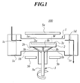
- FIG. 1 is a longitudinal sectional view showing a schematic construction of a vapor phase growth apparatus 100.
- the vapor phase growth apparatus 100 has a reactor 1 in which the silicon single crystal substrate W is disposed.
- the reactor 1 is a reaction chamber having a top wall 1a, a bottom wall 1b and side walls 1e.
- the top wall 1a and the bottom wall 1b are made of translucent quartz.
- a gas supply port 1c for supplying a reaction gas used for vapor phase growth to the reactor 1 inside and a gas exhaust port 1d for exhausting the reaction gas from the reactor 1 are formed.
- a gas supply apparatus (not shown) which supplies a reaction gas with a predetermined composition and flow rate is connected to the gas supply port 1c.
- reaction gas for example, a mixed gas composed of a SiHCl 3 (trichlorosilane) gas as a raw material gas and a H 2 gas as a carrier gas is preferably used in the vapor phase growth of the silicon epitaxial layer on the silicon single crystal substrate.
- SiHCl 3 trichlorosilane
- a heating unit 5a which performs radiation toward the reactor 1 inside through the top wall 1a is installed above the reactor 1 and a heating unit 5b which performs radiation toward the reactor 1 inside through the bottom wall 1b is installed below the reactor 1.
- halogen lamps are used as the heating units 5a and 5b.
- an almost disk-shaped susceptor 2 for placing the silicon single crystal substrate W is disposed in a state of being supported by a supporting member 3.
- the susceptor 2 is one formed by coating graphite with silicon carbide (SiC).
- FIG. 2A A longitudinal sectional view of the susceptor 2 is shown in FIG. 2A.
- the susceptor 2 has a warped inverted U-shaped longitudinal sectional shape.
- a curvature on a rear surface 2b side of the susceptor 2 is 1.75 ⁇ 10 -5 mm -1 or less.
- An almost circular pocket 2c is formed on a main surface 2a, namely, an upper surface of the susceptor 2.
- the pocket 2c is formed to have a double structure having an outer peripheral side part 20 which supports the silicon single crystal substrate W as well as an inner peripheral side part 21 which is formed in a state of being more recessed than the outer peripheral side part 20 in the inside of the outer peripheral side part 20.
- a bottom surface 21a of the pocket 2c namely, a bottom surface 21a of the inner peripheral side part 21 in the pocket 2c is formed to have a U shape in the longitudinal sectional view.
- the bottom surface 21a of the pocket 2c is formed to have a maximum distance of less than 0.4 mm from the rear surface of the silicon single crystal substrate W.
- the maximum distance between the bottom surface 21a of the pocket 2c and the rear surface of the silicon single crystal substrate W is synonymous with the depth within the pocket.
- the depth within the pocket can be obtained from measurement charts drawn up by placing, on a surface table, the susceptor 2 with the main surface side facing up and by performing the measurement in the diametrical parallel using a laser displacement gauge. Further, as shown in FIG. 1, the silicon single crystal substrate W placed within the pocket 2c is heated from above by the heating unit 5a as well as is heated from below through the susceptor 2 by the heating unit 5b, although it is not shown in FIG. 2A.
- FIG. 2B shows a plan view of the rear surface 2b side of the susceptor 2. As shown in this figure, three concave parts 2e which are open to the rear surface of the susceptor 2 are provided in a portion on the outer side than the pocket 2c.
- the supporting member 3 has a rotation shaft 3a vertically extending below the susceptor 2.
- Three spokes 3b which are radially branched obliquely upward are provided on a top end of the rotation shaft 3a. Each end of the spokes 3b is engaged with the concave part 2e of the susceptor 2 to support the susceptor 2.
- a rotary drive device (not shown) is connected to the rotation shaft 3a to allow the rotation shaft 3a and the susceptor 2 to rotate by the drive of the rotary drive device.
- the silicon single crystal substrate is carried and placed within the pocket 2c of the susceptor 2.
- the susceptor 2 is warped in the inverted U shape in a longitudinal sectional view, a distance between the bottom surface 21a of the pocket 2c and the rear surface of the silicon single crystal substrate W is small as compared with a case where the susceptor 2 is warped in the U shape in a longitudinal sectional view.
- the silicon single crystal substrate is heated by the heating units 5a and 5b as well as the susceptor 2 is rotated by the rotary drive device.
- a mixed gas composed of a SiHCl 3 gas and a H 2 gas is introduced as a reaction gas into the reactor 1 from the gas supply port 1c to perform the vapor phase growth.
- the vapor phase growth is performed in a state where a temperature difference between the central part and outer peripheral part on the main surface side of the silicon single crystal substrate W is as small as the distance between the bottom surface 21a of the pocket 2c and the rear surface of the silicon single crystal substrate W decreases as compared with the case of using the U-shaped susceptor in the longitudinal sectional view as described above.
- the vapor phase growth can be performed in a state where a temperature difference between the central part and outer peripheral part on the main surface side of the silicon single crystal substrate W is reduced as compared with the case of using the U-shaped susceptor in the longitudinal sectional view.
- the vapor phase growth can be performed while suppressing thermal stress applied to the outer peripheral part of the silicon single crystal substrate W, so that the occurrence frequency of slip dislocation can be surely reduced.
- Shape of Susceptor means a longitudinal sectional shape of the susceptor, the symbol “U” indicates a U shape and the symbol “ ⁇ ” indicates an inverted U shape.
- the vapor phase growth apparatus 100 as a single wafer type of one is described. Further, as long as the apparatus supports the silicon single crystal substrate W within the pocket in the almost horizontal direction, for example, a batch type of one for performing the vapor phase growth of silicon epitaxial layers on a plurality of the silicon single crystal substrates at the same time, may be used.
- the present invention is similarly applicable also to a silicon single crystal substrate having a diameter of more than 300 mm.
- the vapor phase growth method and the vapor phase growth apparatus according to the present invention are useful for surely reducing the occurrence frequency of the slip dislocation and are suited particularly to a case of the vapor phase growth of the epitaxial layer on the main surface of the silicon single crystal substrate.
Landscapes
- Chemical & Material Sciences (AREA)
- Engineering & Computer Science (AREA)
- Crystallography & Structural Chemistry (AREA)
- Materials Engineering (AREA)
- Metallurgy (AREA)
- Organic Chemistry (AREA)
- Chemical Kinetics & Catalysis (AREA)
- General Chemical & Material Sciences (AREA)
- Chemical Vapour Deposition (AREA)
- Container, Conveyance, Adherence, Positioning, Of Wafer (AREA)
Abstract
Description
- The present invention relates to a vapor phase growth apparatus for performing a vapor phase growth of a silicon epitaxial layer on a main surface of a silicon single crystal substrate, and a vapor phase growth method using the apparatus.
- Conventionally, a so-called single wafer vapor phase growth apparatus is known as an apparatus for growing a silicon epitaxial layer on a main surface of a silicon single crystal substrate. The single wafer vapor phase growth apparatus has an almost disk-shaped susceptor for supporting the silicon single crystal substrate, and can perform a vapor phase growth of the silicon epitaxial layer by heating the silicon single crystal substrate on the susceptor from both sides as well as by feeding silicon raw materials onto a main surface of the substrate. More specifically, the susceptor has a pocket for positioning the silicon single crystal substrate in a central part of the main surface and is designed to support the silicon single crystal substrate within the pocket.
- Incidentally, when the silicon single crystal substrate is nonuniformly heated, slip dislocation easily occurs in the silicon epitaxial layer formed on an upper part of a thermally stressed part of the main surface. Therefore, in order to prevent this slip dislocation from occurring, for example, a susceptor having a pocket of which a bottom surface in the central part is made deeper than that in the outer peripheral part (see, e.g., Japanese Patent Application Publication Unexamined Tokukaisho-61-215289) or a susceptor having a pocket of which a bottom surface is swelled out in a shape of a spherical surface (see, e.g., Japanese Patent Application Publication Unexamined Tokukaisho-62-262417) is used in the vapor phase growth apparatus to uniformly heat the silicon single crystal substrate.
- However, even if the susceptors disclosed in the above-described two documents are used, an occurrence frequency of the slip dislocation varies by individual susceptors. Therefore, the improvement is required so that the occurrence of the slip dislocation can be surely reduced irrespective of differences in susceptors.
- An object of the present invention is to provide a vapor phase growth apparatus capable of surely reducing the occurrence frequency of the slip dislocation and a vapor phase growth method using the apparatus.
- In order to solve these problems, a vapor phase growth apparatus for performing a vapor phase growth of a silicon epitaxial layer on a main surface of a silicon single crystal substrate while heating the silicon single crystal substrate placed on a pocket formed on a susceptor, from both sides, wherein
the pocket has an outer peripheral side part which supports a rear surface of the silicon single crystal substrate and an inner peripheral side part which is kept in a state of being more recessed than the outer peripheral side part in the inside of the outer peripheral side part, and
the susceptor has a warped inverted U-shaped longitudinal sectional shape. - Herein, even if the susceptors having the same type of pocket shape are used, the occurrence frequency of the slip dislocation varies by individual susceptors. The reason why is that in a manufacturing process of susceptors, a part of the susceptors are manufactured to have a warped U shape in a longitudinal sectional view, and as a result, a distance between a rear surface of the silicon single crystal substrate and a bottom surface of the pocket increases.
- More specifically, the susceptor is normally formed by heat-treating a body section composed of graphite to have a high degree of purity and then coating a surface of the body section with SiC (silicon carbide). In the heat-treating, the susceptor is formed to have a warped U shape in a longitudinal sectional view as shown in FIG. 3. Alternatively, the susceptor is formed to have a warped inverted U shape in a longitudinal sectional view as shown in FIG. 2A. Further, in the susceptors disclosed in the above-described two documents, when the susceptor 50 (see FIG.3) with a warped U shape in the longitudinal sectional view is used to perform a vapor phase growth of the silicon epitaxial layer, a distance between a
bottom surface 52 of the pocket and a rear surface of the silicon single crystal substrate W is D+α which is larger than a distance D between the bottom surface of the pocket and the rear surface of the silicon single crystal substrate W in the case of a flat susceptor by an elevation difference α between the position corresponding to a central part of the pocket and the position corresponding to a supporting section of the silicon single crystal substrate W in a rear surface of the susceptor. Accordingly, in this case, a temperature difference between a central part and outer peripheral part on the main surface side of the silicon single crystal substrate W increases and therefore, thermal stress applied to the outer peripheral part of the main surface of the silicon single crystal substrate W increases. As a result, slip dislocation occurs in the silicon epitaxial layer formed on the outer peripheral part. - As described above, the slip dislocation occurs when the distance between the silicon single crystal substrate W and the bottom surface of the inner peripheral side part more recessed than the outer peripheral side part of the pocket which supports the rear surface of the silicon single crystal substrate W increases. Therefore, when the distance decreases, the occurrence frequency of the slip dislocation does not increase.
- Consequently, a
susceptor 2 having a warped inverted U-shaped longitudinal sectional shape as shown in FIG. 2A is selectively used to perform the vapor phase growth in a state where the distance between abottom surface 21a of the pocket and the silicon single crystal substrate W is more reduced than a value D in the case of using aflat susceptor 2 by the amount of warping β. As a result, in this case, as compared with a case of using thesusceptor 50 having a warped U shape in a longitudinal sectional view, a temperature difference between the central part and outer peripheral part on the main surface side of the silicon single crystal substrate W decreases during the vapor phase growth. Further, thermal stress is hardly applied to the outer peripheral part of the silicon single crystal substrate W, and as a result, the occurrence frequency of the slip dislocation can be surely reduced. - When the pocket is formed for a silicon single crystal substrate with a diameter of 300 mm or more, a maximum distance between the bottom surface of the inner peripheral side part in the pocket and the rear surface of the silicon single crystal substrate is preferably less than 0.4 mm. In this case, the occurrence frequency of the slip dislocation can be surely reduced. On the other hand, when the maximum distance between the bottom surface of the inner peripheral side part in the pocket and the rear surface of the silicon single crystal substrate is 0.4 mm or more, the occurrence frequency of the slip dislocation remarkably increases.
- Further, when the susceptor is excessively warped in an inverted U shape in the longitudinal sectional view, the rear surface of the silicon single crystal substrate comes into contact with the bottom surface of the pocket, and as a result, the rear surface of the silicon single crystal substrate is scratched. Particularly, when the rear surface is subjected to mirror surface processing, the scratch stands out and therefore, this susceptor is not preferred.
- In the case where the susceptor is a type of a single wafer, when a warpage size of the inverted U shape is represented by a curvature, the curvature on the rear surface side of the susceptor is preferably 1.75×10⁻⁵ mm-1 or less. When the warpage is as small as this curvature, occurrence of the scratch is prevented from standing out in the rear surface of the substrate, excepting the case where the pocket of the susceptor is extremely shallow. A single wafer susceptor means that the susceptor is used for a single wafer vapor phase growth apparatus. Further, the curvature on the rear surface side of the susceptor is represented by an
inverse number 1/r of a value r calculated from r2=(r-(an elevation difference between the position corresponding to a central part of the pocket and the position corresponding to a supporting section of the silicon single crystal substrate in the rear surface of the susceptor))2+(a radius of the silicon single crystal substrate)2 when representing a curvature radius by r. - Specifically, for example, in the case where the susceptor which is a single wafer one used for a silicon single crystal substrate having a diameter of 300 mm and which is formed such that the distance between the central part of the rear surface of the silicon single crystal substrate and the bottom surface of the inner peripheral side part in the pocket is 0.2 mm in a state where the substrate is not deflected has a warped inverted U shape in a longitudinal sectional view, when a curvature on the rear surface side of the susceptor is larger than 1.75×10⁻⁵ mm-1, the bottom surface of the pocket comes into contact with the rear surface of the silicon single crystal substrate, and as a result, the rear surface of the substrate is scratched.
- Further, the vapor phase growth method of the present invention comprises performing a vapor phase growth of a silicon epitaxial layer on a main surface of a silicon single crystal substrate using the vapor phase growth apparatus of the present invention.
-
- FIG. 1 is a longitudinal sectional view showing a schematic construction of an embodiment of a vapor phase growth apparatus according to the present invention.
- FIG. 2A is a longitudinal sectional view of a susceptor according to the present invention, and FIG. 2B is a plan view showing a rear surface of a susceptor according to the present invention.
- FIG. 3 is a longitudinal sectional view of a conventional susceptor.
- Embodiments of a vapor phase growth apparatus according to the present invention will be described below with reference to the accompanying drawings. The vapor phase growth apparatus of the present embodiment is a single wafer vapor phase growth apparatus for performing a vapor phase growth of an epitaxial layer on a main surface of a silicon single crystal substrate having a diameter of 300 mm.
- FIG. 1 is a longitudinal sectional view showing a schematic construction of a vapor
phase growth apparatus 100. The vaporphase growth apparatus 100 has areactor 1 in which the silicon single crystal substrate W is disposed. - The
reactor 1 is a reaction chamber having a top wall 1a, a bottom wall 1b and side walls 1e. The top wall 1a and the bottom wall 1b are made of translucent quartz. On the side walls 1e, a gas supply port 1c for supplying a reaction gas used for vapor phase growth to thereactor 1 inside and a gas exhaust port 1d for exhausting the reaction gas from thereactor 1 are formed. To the gas supply port 1c, a gas supply apparatus (not shown) which supplies a reaction gas with a predetermined composition and flow rate is connected. As the reaction gas, for example, a mixed gas composed of a SiHCl3 (trichlorosilane) gas as a raw material gas and a H2 gas as a carrier gas is preferably used in the vapor phase growth of the silicon epitaxial layer on the silicon single crystal substrate. - A
heating unit 5a which performs radiation toward thereactor 1 inside through the top wall 1a is installed above thereactor 1 and aheating unit 5b which performs radiation toward thereactor 1 inside through the bottom wall 1b is installed below thereactor 1. In the present embodiment, halogen lamps are used as theheating units - Further, in the
reactor 1, an almost disk-shaped susceptor 2 for placing the silicon single crystal substrate W is disposed in a state of being supported by a supporting member 3. - The
susceptor 2 is one formed by coating graphite with silicon carbide (SiC). - A longitudinal sectional view of the
susceptor 2 is shown in FIG. 2A. As shown in this figure, thesusceptor 2 has a warped inverted U-shaped longitudinal sectional shape. A curvature on arear surface 2b side of thesusceptor 2 is 1.75×10⁻⁵ mm-1 or less. An almostcircular pocket 2c is formed on amain surface 2a, namely, an upper surface of thesusceptor 2. - The
pocket 2c is formed to have a double structure having an outerperipheral side part 20 which supports the silicon single crystal substrate W as well as an innerperipheral side part 21 which is formed in a state of being more recessed than the outerperipheral side part 20 in the inside of the outerperipheral side part 20. Abottom surface 21a of thepocket 2c, namely, abottom surface 21a of the innerperipheral side part 21 in thepocket 2c is formed to have a U shape in the longitudinal sectional view. In more detail, thebottom surface 21a of thepocket 2c is formed to have a maximum distance of less than 0.4 mm from the rear surface of the silicon single crystal substrate W. In the present embodiment, the maximum distance between thebottom surface 21a of thepocket 2c and the rear surface of the silicon single crystal substrate W is synonymous with the depth within the pocket. The depth within the pocket can be obtained from measurement charts drawn up by placing, on a surface table, thesusceptor 2 with the main surface side facing up and by performing the measurement in the diametrical parallel using a laser displacement gauge. Further, as shown in FIG. 1, the silicon single crystal substrate W placed within thepocket 2c is heated from above by theheating unit 5a as well as is heated from below through thesusceptor 2 by theheating unit 5b, although it is not shown in FIG. 2A. - Further, FIG. 2B shows a plan view of the
rear surface 2b side of thesusceptor 2. As shown in this figure, threeconcave parts 2e which are open to the rear surface of thesusceptor 2 are provided in a portion on the outer side than thepocket 2c. - As shown in FIG. 1, the supporting member 3 has a
rotation shaft 3a vertically extending below thesusceptor 2. Threespokes 3b which are radially branched obliquely upward are provided on a top end of therotation shaft 3a. Each end of thespokes 3b is engaged with theconcave part 2e of thesusceptor 2 to support thesusceptor 2. A rotary drive device (not shown) is connected to therotation shaft 3a to allow therotation shaft 3a and thesusceptor 2 to rotate by the drive of the rotary drive device. - Next, a vapor phase growth method for performing the vapor phase growth of a silicon epitaxial layer on a silicon single crystal substrate using the above-described vapor
phase growth apparatus 100 will be described. - First, the silicon single crystal substrate is carried and placed within the
pocket 2c of thesusceptor 2. Herein, since thesusceptor 2 is warped in the inverted U shape in a longitudinal sectional view, a distance between thebottom surface 21a of thepocket 2c and the rear surface of the silicon single crystal substrate W is small as compared with a case where thesusceptor 2 is warped in the U shape in a longitudinal sectional view. - Next, the silicon single crystal substrate is heated by the
heating units susceptor 2 is rotated by the rotary drive device. In this state, a mixed gas composed of a SiHCl3 gas and a H2 gas is introduced as a reaction gas into thereactor 1 from the gas supply port 1c to perform the vapor phase growth. At this time, the vapor phase growth is performed in a state where a temperature difference between the central part and outer peripheral part on the main surface side of the silicon single crystal substrate W is as small as the distance between thebottom surface 21a of thepocket 2c and the rear surface of the silicon single crystal substrate W decreases as compared with the case of using the U-shaped susceptor in the longitudinal sectional view as described above. - According to the above-described vapor
phase growth apparatus 100, the vapor phase growth can be performed in a state where a temperature difference between the central part and outer peripheral part on the main surface side of the silicon single crystal substrate W is reduced as compared with the case of using the U-shaped susceptor in the longitudinal sectional view. In other words, the vapor phase growth can be performed while suppressing thermal stress applied to the outer peripheral part of the silicon single crystal substrate W, so that the occurrence frequency of slip dislocation can be surely reduced. - Further, when the maximum distance between the
bottom surface 21a of thepocket 2c and the rear surface of the silicon single crystal substrate W, namely, the depth within the pocket is less than 0.4 mm, the occurrence frequency of the slip dislocation can be surely reduced as shown in the following Table 1.[Table 1] Shape of Susceptor ∩ ∩ ∩ ∩ ∩ Depth within Pocket (mm) 0.23 0.32 0.38 0.48 0.53 Occurrence of Slip Dislocation ○ ○ ○ × ○ (○: no slip dislocation occurs, ×: slip dislocation occurs) - In the table, the term "Shape of Susceptor" means a longitudinal sectional shape of the susceptor, the symbol "U" indicates a U shape and the symbol "∩" indicates an inverted U shape.
- In the above-described embodiment, the vapor
phase growth apparatus 100 as a single wafer type of one is described. Further, as long as the apparatus supports the silicon single crystal substrate W within the pocket in the almost horizontal direction, for example, a batch type of one for performing the vapor phase growth of silicon epitaxial layers on a plurality of the silicon single crystal substrates at the same time, may be used. - Further, a case of the vapor phase growth of the silicon epitaxial layer on the main surface of the silicon single crystal substrate having a diameter of 300 mm is described. As a diameter of the silicon single crystal substrate is larger, a depth within the pocket must be more reduced in order to reduce slip dislocation, and therefore, the present invention is similarly applicable also to a silicon single crystal substrate having a diameter of more than 300 mm.
- As described above, the vapor phase growth method and the vapor phase growth apparatus according to the present invention are useful for surely reducing the occurrence frequency of the slip dislocation and are suited particularly to a case of the vapor phase growth of the epitaxial layer on the main surface of the silicon single crystal substrate.
Claims (4)
- A vapor phase growth apparatus for performing a vapor phase growth of a silicon epitaxial layer on a main surface of a silicon single crystal substrate while heating the silicon single crystal substrate placed on a pocket formed on a susceptor, from both sides, wherein
the pocket has an outer peripheral side part which supports a rear surface of the silicon single crystal substrate and an inner peripheral side part which is kept in a state of being more recessed than the outer peripheral side part in an inside of the outer peripheral side part, and
the susceptor has a warped inverted U-shaped longitudinal sectional shape. - The vapor phase growth apparatus as claimed in claim 1, wherein
the pocket is formed for a silicon single crystal substrate having a diameter of 300 mm or more, and
a maximum distance between a bottom surface of the inner peripheral side part in the pocket and a rear surface of the silicon single crystal substrate is less than 0.4 mm. - The vapor phase growth apparatus as claimed in claim 1 or 2, wherein
the susceptor is a type of a single wafer, and a curvature on a rear surface side of the susceptor is 1.75×10⁻⁵ mm-1 or less. - A vapor phase growth method, comprising performing a vapor phase growth of a silicon epitaxial layer on a main surface of a silicon single crystal substrate using the vapor phase growth apparatus as claimed in any one of claims 1 to 3.
Applications Claiming Priority (2)
| Application Number | Priority Date | Filing Date | Title |
|---|---|---|---|
| JP2003284912A JP4599816B2 (en) | 2003-08-01 | 2003-08-01 | Manufacturing method of silicon epitaxial wafer |
| PCT/JP2004/006007 WO2005013343A1 (en) | 2003-08-01 | 2004-04-26 | Vapor deposition apparatus and vapor deposition method |
Publications (3)
| Publication Number | Publication Date |
|---|---|
| EP1650788A1 true EP1650788A1 (en) | 2006-04-26 |
| EP1650788A4 EP1650788A4 (en) | 2006-10-11 |
| EP1650788B1 EP1650788B1 (en) | 2010-07-14 |
Family
ID=34113856
Family Applications (1)
| Application Number | Title | Priority Date | Filing Date |
|---|---|---|---|
| EP04729522A Expired - Lifetime EP1650788B1 (en) | 2003-08-01 | 2004-04-26 | Method for manufacturing a silicon epitaxial wafer |
Country Status (6)
| Country | Link |
|---|---|
| US (1) | US7591908B2 (en) |
| EP (1) | EP1650788B1 (en) |
| JP (1) | JP4599816B2 (en) |
| KR (1) | KR101079175B1 (en) |
| DE (1) | DE602004028126D1 (en) |
| WO (1) | WO2005013343A1 (en) |
Families Citing this family (16)
| Publication number | Priority date | Publication date | Assignee | Title |
|---|---|---|---|---|
| JP2010016312A (en) * | 2008-07-07 | 2010-01-21 | Sumco Corp | Method for manufacturing epitaxial wafer |
| TWI397113B (en) * | 2008-08-29 | 2013-05-21 | 維克儀器公司 | Wafer carrier with variable thermal resistance |
| US20100107974A1 (en) * | 2008-11-06 | 2010-05-06 | Asm America, Inc. | Substrate holder with varying density |
| JP5521561B2 (en) * | 2010-01-12 | 2014-06-18 | 信越半導体株式会社 | Manufacturing method of bonded wafer |
| US9650726B2 (en) * | 2010-02-26 | 2017-05-16 | Applied Materials, Inc. | Methods and apparatus for deposition processes |
| CN101979721A (en) * | 2010-09-19 | 2011-02-23 | 山东伟基炭科技有限公司 | Silicon core rods and silicon core structure for growth of polycrystalline silicon |
| TWI541928B (en) * | 2011-10-14 | 2016-07-11 | 晶元光電股份有限公司 | Wafer carrier |
| US10316412B2 (en) | 2012-04-18 | 2019-06-11 | Veeco Instruments Inc. | Wafter carrier for chemical vapor deposition systems |
| CN102828238B (en) * | 2012-08-24 | 2015-11-04 | 东莞市中镓半导体科技有限公司 | For improveing the method for substrate wafer surface temperature field in epitaxial process |
| US9799548B2 (en) * | 2013-03-15 | 2017-10-24 | Applied Materials, Inc. | Susceptors for enhanced process uniformity and reduced substrate slippage |
| US10167571B2 (en) | 2013-03-15 | 2019-01-01 | Veeco Instruments Inc. | Wafer carrier having provisions for improving heating uniformity in chemical vapor deposition systems |
| ITCO20130041A1 (en) * | 2013-09-27 | 2015-03-28 | Lpe Spa | SUSCECTOR WITH SUPPORT ELEMENT |
| DE102014100024A1 (en) | 2014-01-02 | 2015-07-02 | Aixtron Se | Device for the arrangement of substrates, in particular susceptor of a CVD reactor |
| CN105917459A (en) * | 2014-02-07 | 2016-08-31 | 应用材料公司 | Chucking capability for bowed wafers on DSA |
| WO2018207942A1 (en) * | 2017-05-12 | 2018-11-15 | 東洋炭素株式会社 | Susceptor, method for producing epitaxial substrate, and epitaxial substrate |
| JP7296914B2 (en) * | 2020-04-17 | 2023-06-23 | 三菱電機株式会社 | Method for manufacturing satellite and silicon carbide semiconductor device |
Family Cites Families (21)
| Publication number | Priority date | Publication date | Assignee | Title |
|---|---|---|---|---|
| JPS58182819A (en) * | 1982-04-20 | 1983-10-25 | Toshiba Corp | Heating base |
| JPS5932123A (en) * | 1982-08-18 | 1984-02-21 | Sony Corp | Vapor growth method |
| JPS61215289A (en) | 1985-03-19 | 1986-09-25 | Toshiba Mach Co Ltd | Vapor-phase growth apparatus |
| JPS62262417A (en) | 1986-05-09 | 1987-11-14 | Toshiba Mach Co Ltd | Susceptor for vapor growth |
| JPH01256118A (en) | 1988-04-05 | 1989-10-12 | Sumitomo Metal Ind Ltd | Vapor phase reaction equipment |
| JPH03150365A (en) * | 1989-07-26 | 1991-06-26 | Tokyo Electron Ltd | Heat treating device |
| IL100910A (en) * | 1991-02-12 | 1994-10-07 | Hughes Aircraft Co | Evaluation of the extent of wear of articles |
| JPH0555151A (en) * | 1991-08-23 | 1993-03-05 | Fujitsu Ltd | Semiconductor manufacturing apparatus |
| US5444217A (en) * | 1993-01-21 | 1995-08-22 | Moore Epitaxial Inc. | Rapid thermal processing apparatus for processing semiconductor wafers |
| JPH06302550A (en) * | 1993-04-13 | 1994-10-28 | Hitachi Ltd | Semiconductor manufacturing equipment |
| JP3317781B2 (en) * | 1994-06-08 | 2002-08-26 | 東芝セラミックス株式会社 | Method of manufacturing susceptor for heat treatment of semiconductor wafer |
| FR2766845B1 (en) * | 1997-07-31 | 1999-10-15 | Sgs Thomson Microelectronics | EPITAXY PROCESS ON A SILICON SUBSTRATE COMPRISING AREAS HIGHLY DOPED WITH ARSENIC |
| WO1999023690A1 (en) * | 1997-11-03 | 1999-05-14 | Asm America, Inc. | Method of processing wafers with low mass support |
| US6026589A (en) * | 1998-02-02 | 2000-02-22 | Silicon Valley Group, Thermal Systems Llc | Wafer carrier and semiconductor apparatus for processing a semiconductor substrate |
| JP4003906B2 (en) * | 1999-03-19 | 2007-11-07 | コバレントマテリアル株式会社 | Silicon single crystal semiconductor wafer heat treatment jig and silicon single crystal semiconductor wafer heat treatment apparatus using the same |
| JP3424069B2 (en) * | 1999-04-28 | 2003-07-07 | 東芝セラミックス株式会社 | Manufacturing method of epitaxial silicon substrate |
| JP2000355766A (en) * | 1999-06-15 | 2000-12-26 | Hitachi Kokusai Electric Inc | Substrate processing apparatus and substrate processing method |
| CA2327201A1 (en) * | 1999-12-02 | 2001-06-02 | Masaharu Amano | Bucket tooth and method of manufacturing the same |
| JP2002134484A (en) * | 2000-10-19 | 2002-05-10 | Asm Japan Kk | Semiconductor substrate holding device |
| JP2003203866A (en) * | 2001-10-24 | 2003-07-18 | Shin Etsu Handotai Co Ltd | Vapor growth apparatus and method of manufacturing epitaxial wafer |
| JP3514254B2 (en) | 2001-12-28 | 2004-03-31 | 信越半導体株式会社 | Heat treatment apparatus and method for manufacturing silicon epitaxial wafer |
-
2003
- 2003-08-01 JP JP2003284912A patent/JP4599816B2/en not_active Expired - Fee Related
-
2004
- 2004-04-26 US US10/565,653 patent/US7591908B2/en not_active Expired - Lifetime
- 2004-04-26 EP EP04729522A patent/EP1650788B1/en not_active Expired - Lifetime
- 2004-04-26 KR KR1020067002089A patent/KR101079175B1/en not_active Expired - Fee Related
- 2004-04-26 WO PCT/JP2004/006007 patent/WO2005013343A1/en not_active Ceased
- 2004-04-26 DE DE602004028126T patent/DE602004028126D1/en not_active Expired - Lifetime
Also Published As
| Publication number | Publication date |
|---|---|
| EP1650788B1 (en) | 2010-07-14 |
| KR20060052948A (en) | 2006-05-19 |
| JP2005056984A (en) | 2005-03-03 |
| DE602004028126D1 (en) | 2010-08-26 |
| KR101079175B1 (en) | 2011-11-02 |
| WO2005013343A1 (en) | 2005-02-10 |
| EP1650788A4 (en) | 2006-10-11 |
| US7591908B2 (en) | 2009-09-22 |
| US20060180076A1 (en) | 2006-08-17 |
| JP4599816B2 (en) | 2010-12-15 |
Similar Documents
| Publication | Publication Date | Title |
|---|---|---|
| EP1650788B1 (en) | Method for manufacturing a silicon epitaxial wafer | |
| KR100893909B1 (en) | A method of manufacturing a substrate holder | |
| EP1456871B1 (en) | Susceptor for epitaxial growth | |
| US8021968B2 (en) | Susceptor and method for manufacturing silicon epitaxial wafer | |
| JP3204699B2 (en) | Heat treatment equipment | |
| JP3090339B2 (en) | Vapor growth apparatus and method | |
| EP1615259A1 (en) | Susceptor and vapor growth device | |
| US5516283A (en) | Apparatus for processing a plurality of circular wafers | |
| US20050092439A1 (en) | Low/high temperature substrate holder to reduce edge rolloff and backside damage | |
| US20100107974A1 (en) | Substrate holder with varying density | |
| CN1653591A (en) | Process and system for heating semiconductor substrates in a processing chamber containing a susceptor | |
| JPH08181080A (en) | Substrate support device for chemical vapor deposition | |
| US20040144323A1 (en) | Epitaxial wafer production apparatus and susceptor structure | |
| US8317449B2 (en) | Multiple substrate transfer robot | |
| US20090139448A1 (en) | Vapor phase growth apparatus ans vapor phase growth method | |
| EP1535314A2 (en) | High rate deposition at low pressures in a small batch reactor | |
| WO2004008493A2 (en) | Method and apparatus for supporting semiconductor wafers | |
| WO1996030564A1 (en) | Method and apparatus for configuring an epitaxial reactor for reduced set-up time and improved layer quality | |
| JP3004846B2 (en) | Susceptor for vapor phase growth equipment | |
| JP2003197553A (en) | Heat treatment boat and vertical heat treatment equipment | |
| EP2385153A1 (en) | Cvd apparatus | |
| EP1533834B1 (en) | Vapor phase epitaxial apparatus and vapor phase epitaxial method | |
| TWI853310B (en) | Method for manufacturing epitaxial wafer and epitaxial wafer manufacturing device | |
| JP3603216B2 (en) | Thin film growth equipment | |
| JP2005235906A (en) | Wafer holding jig and vapor phase growing apparatus |
Legal Events
| Date | Code | Title | Description |
|---|---|---|---|
| PUAI | Public reference made under article 153(3) epc to a published international application that has entered the european phase |
Free format text: ORIGINAL CODE: 0009012 |
|
| 17P | Request for examination filed |
Effective date: 20060201 |
|
| AK | Designated contracting states |
Kind code of ref document: A1 Designated state(s): DE |
|
| A4 | Supplementary search report drawn up and despatched |
Effective date: 20060912 |
|
| DAX | Request for extension of the european patent (deleted) | ||
| RBV | Designated contracting states (corrected) |
Designated state(s): DE |
|
| RAP1 | Party data changed (applicant data changed or rights of an application transferred) |
Owner name: SHIN-ETSU HANDOTAI CO., LTD. |
|
| 17Q | First examination report despatched |
Effective date: 20090619 |
|
| RTI1 | Title (correction) |
Free format text: METHOD FOR MANUFACTURING A SILICON EPITAXIAL WAFER |
|
| GRAP | Despatch of communication of intention to grant a patent |
Free format text: ORIGINAL CODE: EPIDOSNIGR1 |
|
| RTI1 | Title (correction) |
Free format text: METHOD FOR MANUFACTURING A SILICON EPITAXIAL WAFER |
|
| GRAS | Grant fee paid |
Free format text: ORIGINAL CODE: EPIDOSNIGR3 |
|
| GRAA | (expected) grant |
Free format text: ORIGINAL CODE: 0009210 |
|
| RIN1 | Information on inventor provided before grant (corrected) |
Inventor name: KANNO, TAKAO,C/O SHIN-ETSU HANDOTAI CO. LTD. Inventor name: KANAYA, KOICHI,C/O SHIN-ETSU HANDOTAI CO. LTD. Inventor name: OTSUKA, TORU,C/O SHIN-ETSU HANDOTAI CO. LTD. |
|
| AK | Designated contracting states |
Kind code of ref document: B1 Designated state(s): DE |
|
| REF | Corresponds to: |
Ref document number: 602004028126 Country of ref document: DE Date of ref document: 20100826 Kind code of ref document: P |
|
| PLBE | No opposition filed within time limit |
Free format text: ORIGINAL CODE: 0009261 |
|
| STAA | Information on the status of an ep patent application or granted ep patent |
Free format text: STATUS: NO OPPOSITION FILED WITHIN TIME LIMIT |
|
| 26N | No opposition filed |
Effective date: 20110415 |
|
| REG | Reference to a national code |
Ref country code: DE Ref legal event code: R097 Ref document number: 602004028126 Country of ref document: DE Effective date: 20110415 |
|
| PGFP | Annual fee paid to national office [announced via postgrant information from national office to epo] |
Ref country code: DE Payment date: 20220302 Year of fee payment: 19 |
|
| REG | Reference to a national code |
Ref country code: DE Ref legal event code: R119 Ref document number: 602004028126 Country of ref document: DE |
|
| PG25 | Lapsed in a contracting state [announced via postgrant information from national office to epo] |
Ref country code: DE Free format text: LAPSE BECAUSE OF NON-PAYMENT OF DUE FEES Effective date: 20231103 |