EP1650647B1 - Hybrid adder comprising multiple sub-adders, each of which uses a different carry propagation scheme - Google Patents
Hybrid adder comprising multiple sub-adders, each of which uses a different carry propagation scheme Download PDFInfo
- Publication number
- EP1650647B1 EP1650647B1 EP05011528A EP05011528A EP1650647B1 EP 1650647 B1 EP1650647 B1 EP 1650647B1 EP 05011528 A EP05011528 A EP 05011528A EP 05011528 A EP05011528 A EP 05011528A EP 1650647 B1 EP1650647 B1 EP 1650647B1
- Authority
- EP
- European Patent Office
- Prior art keywords
- adder
- carry
- mixed
- sub
- scheme
- Prior art date
- Legal status (The legal status is an assumption and is not a legal conclusion. Google has not performed a legal analysis and makes no representation as to the accuracy of the status listed.)
- Expired - Lifetime
Links
Images


Classifications
-
- G—PHYSICS
- G06—COMPUTING OR CALCULATING; COUNTING
- G06F—ELECTRIC DIGITAL DATA PROCESSING
- G06F7/00—Methods or arrangements for processing data by operating upon the order or content of the data handled
- G06F7/38—Methods or arrangements for performing computations using exclusively denominational number representation, e.g. using binary, ternary, decimal representation
- G06F7/48—Methods or arrangements for performing computations using exclusively denominational number representation, e.g. using binary, ternary, decimal representation using non-contact-making devices, e.g. tube, solid state device; using unspecified devices
- G06F7/50—Adding; Subtracting
-
- G—PHYSICS
- G06—COMPUTING OR CALCULATING; COUNTING
- G06F—ELECTRIC DIGITAL DATA PROCESSING
- G06F7/00—Methods or arrangements for processing data by operating upon the order or content of the data handled
- G06F7/38—Methods or arrangements for performing computations using exclusively denominational number representation, e.g. using binary, ternary, decimal representation
- G06F7/48—Methods or arrangements for performing computations using exclusively denominational number representation, e.g. using binary, ternary, decimal representation using non-contact-making devices, e.g. tube, solid state device; using unspecified devices
- G06F7/50—Adding; Subtracting
- G06F7/505—Adding; Subtracting in bit-parallel fashion, i.e. having a different digit-handling circuit for each denomination
- G06F7/506—Adding; Subtracting in bit-parallel fashion, i.e. having a different digit-handling circuit for each denomination with simultaneous carry generation for, or propagation over, two or more stages
-
- G—PHYSICS
- G06—COMPUTING OR CALCULATING; COUNTING
- G06F—ELECTRIC DIGITAL DATA PROCESSING
- G06F7/00—Methods or arrangements for processing data by operating upon the order or content of the data handled
- G06F7/38—Methods or arrangements for performing computations using exclusively denominational number representation, e.g. using binary, ternary, decimal representation
- G06F7/48—Methods or arrangements for performing computations using exclusively denominational number representation, e.g. using binary, ternary, decimal representation using non-contact-making devices, e.g. tube, solid state device; using unspecified devices
- G06F7/50—Adding; Subtracting
- G06F7/505—Adding; Subtracting in bit-parallel fashion, i.e. having a different digit-handling circuit for each denomination
- G06F7/506—Adding; Subtracting in bit-parallel fashion, i.e. having a different digit-handling circuit for each denomination with simultaneous carry generation for, or propagation over, two or more stages
- G06F7/507—Adding; Subtracting in bit-parallel fashion, i.e. having a different digit-handling circuit for each denomination with simultaneous carry generation for, or propagation over, two or more stages using selection between two conditionally calculated carry or sum values
-
- G—PHYSICS
- G06—COMPUTING OR CALCULATING; COUNTING
- G06F—ELECTRIC DIGITAL DATA PROCESSING
- G06F7/00—Methods or arrangements for processing data by operating upon the order or content of the data handled
- G06F7/38—Methods or arrangements for performing computations using exclusively denominational number representation, e.g. using binary, ternary, decimal representation
- G06F7/48—Methods or arrangements for performing computations using exclusively denominational number representation, e.g. using binary, ternary, decimal representation using non-contact-making devices, e.g. tube, solid state device; using unspecified devices
- G06F7/50—Adding; Subtracting
- G06F7/505—Adding; Subtracting in bit-parallel fashion, i.e. having a different digit-handling circuit for each denomination
- G06F7/506—Adding; Subtracting in bit-parallel fashion, i.e. having a different digit-handling circuit for each denomination with simultaneous carry generation for, or propagation over, two or more stages
- G06F7/508—Adding; Subtracting in bit-parallel fashion, i.e. having a different digit-handling circuit for each denomination with simultaneous carry generation for, or propagation over, two or more stages using carry look-ahead circuits
Definitions
- the present invention relates to a digital integrated circuit for performing an arithmetic operation, particularly, an adder, and more particularly to an adder with optimized design costs.
- a binary adding operation which is most frequently used in digital systems, plays an essential role in designing general-purpose processors, special-purpose processors such as digital signal processors, and almost all application-specific integrated circuits (ASIC).
- ASIC application-specific integrated circuits
- an adder which is a basic element for performing large-scale, complicated operations, such as multiplication, division, and floating-point operations, is used in various design units such as a memory address generator or a program counter, it is an important design issue to develop binary adders with optimal design costs.
- Fig. 1 is a block diagram of the ripple carry adder. Equations 1 and 2 are equations for signals s i and c i using signal bits x i and y i shown in Fig. 1 .
- a symbol '+' represents a binary OR operation
- a symbol ' ⁇ ' represents a binary AND operation
- a symbol "' is a unary operator for performing a binary NOT operation.
- a high speed adder commonly used includes a carry skip adder, a carry select adder, a carry lookahead adder, etc. In such adders, the amount of silicon circuits used has been increased in correspondence with increased speed of the add operation.
- a mixed-type adder which includes a carry generation layer employing a carry lookahead scheme for high speed carry propagation and a sum generation layer employing a carry select scheme for calculating a sum quickly through carry prediction, has been used for high speed add operations.
- Fig. 2 is a diagram illustrating a structure of a mixed-type adder employing both the carry lookahead scheme and the carry select scheme.
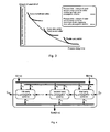
- Fig. 3 solid lines represent trade-off design spaces for a relationship of delay time-amount of used circuits of an adder, which is attained when a conventional adder structure is used.
- Delay time-amount of used circuits curves showing trade-off characteristics are formed depending on the kind of adder, and curvatures of the delay time-amount of used circuit curves can be determined by a degree of optimization applied to each adder.
- Each of delay time-amount of used circuits curves has an ideal banana-shaped inverse-proportional plot.
- the delay time-amount of used circuits curves do not have the ideal banana-shaped inverse-proportional plot if each of the delay time-amount of used circuit curves forms a single delay time-amount of used circuit curve.
- the delay time-amount of used circuit curves have a non-ideal stepped trade-off curve from an overall point of view. Since the delay time and the amount of used circuits do not have an accurate inverse-proportional relationship in such a non-ideal trade-off curve, even when restrictions on the delay time of adder are alleviated, the amount of used circuits cannot be reduced, which results in ineffective optimization of the adder design. Accordingly, there is a need for a method for obtaining an ideal and effective trade-off curve, as indicated by a dotted line in Fig. 3 , in optimization of the relationship of the delay time and the amount of used circuits.
- BEHROOZ PARHAMI "COMPUTER ARITHMETIC" 2000, OXFORD UNIVERSITY PRESS , NEW YORK , XP002354483, pages 108-120 illustrates a carry select adder made of a plurality of carry look ahead blocks.
- EP-A-0 590 251 discloses another high speed adder made of a plurality of groups of sub-adders being connected in series in the carry path, all being of different carry look ahead scheme.
- the present invention has been made in view of the problems of the conventional method, and it is an object of the present invention to provide an adder with optimized design costs.
- a mixed-type adder including I sub adders, (where, I is a positive number larger than 1), wherein an overall bit width of the mixed-type adder is divided into I bit groups of different bit width which are respectively allocated to the I sub adders, the I sub adders having different carry propagation schemes said carry propagation scheme being selected among the carry look ahead adder scheme, the carry skip adder scheme and the ripple carry adder scheme, and connected in series through a carry signal.
- Each of the sub adders composing the mixed-type adder could be a mixed-type binary adder or a mixed-type adder having a different digital representation.
- the mixed-type adder could use an adder intellectual property (IP) having bit width parameters adjusted such that the sum of width of I bits is the overall bit width.
- IP adder intellectual property
- FIG. 4 is a block diagram of a structure of a mixed-type binary adder of a multi carry propagation scheme according to a preferred embodiment of the present invention.
- a mixed-type binary adder of a multi carry propagation scheme has a structure wherein a plurality binary adders of a single carry propagation scheme are connected to each other by means of carry signals.
- An n-bit adder having a structure where a plurality ('I' in the figure) of sub adders designed according to different carry propagation schemes are connected in series receives two numbers A and B, each having n bits, and a carry input signal C in and calculates a sum output signal Sum, which represents a sum of the two numbers, and a carry output signal C out .
- the overall bit width of an adder to be designed is divided into a plurality of bit groups, n 1 , n 2 , ..., n I , to which particular carry propagation schemes are applied.
- Fig. 4 shows a carry propagation scheme applied to each sub adder and a bit width assigned to each sub adder.
- Fig. 5 is a schematic block diagram of a mixed-type adder according to a more detailed embodiment of the present invention.
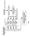
- the mixed-type binary adder of the multi carry propagation scheme as shown in Fig. 5 has a structure where three sub adders, i.e., a ripple carry adder, a carry skip adder, and a carry lookahead adder, are connected in series by means of a carry signal.
- the sub adders employable for implementing the mixed-type adder according to the present invention are not limited to this.
- the carry lookahead adder has an n 1 bit width
- the carry skip adder has an n 2 bit width
- the ripple lookahead adder has an n 3 bit width.
- n 1 + n 2 + n 3 n.
- the structure of the mixed-type binary adder of the multi carry propagation scheme according to the present invention can be designed using various adder intellectual properties (IP) in an IP library.
- Fig. 6 is a diagram showing a design flow for the mixed-type binary adder of the multi carry propagation scheme using the adder IPs in the IP library.
- the mixed-type binary adder of the multi carry propagation scheme according to the present invention can be configured using the IP library by sequentially connecting adder codes (soft IPs prepared using design languages such as VHDL or Verilog), which are generated after adjusting bit width parameters of the binary adders of various single carry propagation schemes present in the existing IP library, by means of the carry signal.
- adder codes soft IPs prepared using design languages such as VHDL or Verilog
- a first method is to design the structure of the mixed-type binary adder such that the amount of used circuits is minimized under given restrictions on delay time. That is, the amount of used circuits is minimized by positioning a process time of an adder on a particular time interval.
- Such a design is used when an adder circuit optimized for a preset cycle time is designed after a cycle time of a system to be designed is fixed.
- a process time of the mixed-type binary adder employing the multi carry propagation scheme can be predicted with the sum of add process times of a plurality of sub adders employing respective single carry propagation schemes and composing the mixed-type binary adder employing the multi carry propagation scheme.
- the amount of used circuits can also be predicted with the sum of the amount of used circuits of a plurality of sub adders employing respective single carry propagation schemes and composing the mixed-type binary adder employing the multi carry propagation scheme.
- T is expressed by the sum of process times T i (i is a subscript used to distinguish among 'I' different carry propagation schemes and has range values of 1 to I) of sub adders employing 'I' carry propagation schemes.
- amount of used circuits A of the mixed-type binary adder employing 'I' multi carry propagation schemes is expressed by the sum of the amount of used circuits A i of sub adders employing 'I' carry propagation schemes.
- T and A can be expressed as follows.
- a second method is to design the structure of the mixed-type binary adder such that the delay time is minimized under restrictions on the amount of used circuits that the minimal value of the amount of used circuits is 1b and the maximal value of the amount of used circuits is ub.
- the minimization of the delay time is expressed as follows.
- the minimization of the amount of used circuits under the restrictions on the delay time and the minimization of the delay time under the restrictions on the amount of used circuits can be implemented through simulation annealing, a heuristic algorithm such as a genetic algorithm, and linear programming .
- a design curve for the relationship between the delay time and the amount of used circuits is prepared by linearly combining the ripple carry adder, the carry skip adder and the carry lookahead adder.
- the ripple carry adder is very slow its operational speed although the amount of used circuits thereof is small, and the carry lookahead adder is very fast in its operational speed although the amount of used circuits thereof is large.
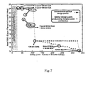
- Fig. 7 is a diagram showing a curve for providing a trade-off between the amount of used circuits and the process time of a 128 bits mixed-type binary adder, which is provided to show a merit of the adder according to the present invention.
- a horizontal axis represents the process time in the unit of propagation time of a fanout-4 inverter and a vertical axis represents the amount of used circuits in the unit of amount of used circuits of the fanout-4 inverter.
- Points indicated by '+' correspond to a design plotted by the dotted line in Fig. 3 , showing optimization designs created according to the present invention.
- Points indicated by ' " ' correspond to the designs plotted by the solid lines in Fig.
- a set of optimal designs indicated by (2) includes design created according to the present invention.
- the set of optimal designs indicated by 2 according to the present invention has the amount of used circuits smaller than that of a set of designs indicated by 1, which is created according to the existing design schemes.
- the mixed-type binary adder has the small amount of used circuits, compared to the existing design schemes.
Landscapes
- Physics & Mathematics (AREA)
- General Physics & Mathematics (AREA)
- Engineering & Computer Science (AREA)
- Computational Mathematics (AREA)
- Mathematical Analysis (AREA)
- Pure & Applied Mathematics (AREA)
- Theoretical Computer Science (AREA)
- Computing Systems (AREA)
- Mathematical Optimization (AREA)
- General Engineering & Computer Science (AREA)
- Design And Manufacture Of Integrated Circuits (AREA)
Description
- The present invention relates to a digital integrated circuit for performing an arithmetic operation, particularly, an adder, and more particularly to an adder with optimized design costs.
- A binary adding operation, which is most frequently used in digital systems, plays an essential role in designing general-purpose processors, special-purpose processors such as digital signal processors, and almost all application-specific integrated circuits (ASIC). Moreover, since an adder, which is a basic element for performing large-scale, complicated operations, such as multiplication, division, and floating-point operations, is used in various design units such as a memory address generator or a program counter, it is an important design issue to develop binary adders with optimal design costs.
- Numerous studies on various kinds of carry propagation schemes, which are a main design factor of the digital system, taking into consideration operation speed of circuits, amount of silicon used, and power consumption according to design goals, have been conducted. Until high performance adders were developed, early digital systems used a ripple carry adder of the simplest form.
Fig. 1 is a block diagram of the ripple carry adder.Equations 1 and 2 are equations for signals si and ci using signal bits xi and yi shown inFig. 1 .

- In the above equations, a symbol '+' represents a binary OR operation, and a symbol '·' represents a binary AND operation. A symbol "' is a unary operator for performing a binary NOT operation. Although the ripple carry adder can perform an add operation using a small quantity of silicon, it is very slow in performing the add operation since carry propagation in the adder is linear.
- For a higher speed adder, there are many cases where a carry prediction circuit is used to accelerate carry generation and propagation, or a carry propagation path for faster carry propagation is implemented with a multi-layered binary tree structure. A high speed adder commonly used includes a carry skip adder, a carry select adder, a carry lookahead adder, etc. In such adders, the amount of silicon circuits used has been increased in correspondence with increased speed of the add operation.
- When an adder is implemented with a multi-layered structure, various carry propagation schemes are applicable to different layers. As suggested in "Carry-Lookahead/Carry-Select Binary Adder,
US Patent - 5,508,952, Apr. 16, 1996 " and "Adder Which Employs Both Carry Look-Ahead and Carry Select Techniques,US Patent - 5,898,596 Apr. 27, 1999 ", a mixed-type adder, which includes a carry generation layer employing a carry lookahead scheme for high speed carry propagation and a sum generation layer employing a carry select scheme for calculating a sum quickly through carry prediction, has been used for high speed add operations.Fig. 2 is a diagram illustrating a structure of a mixed-type adder employing both the carry lookahead scheme and the carry select scheme. - In conventional adder designs, a single carry propagation scheme has been mainly used, and many different optimization techniques including an optimization at a transistor level, application of an asynchronous design scheme, an optimization of a bit width employing the carry prediction scheme, etc., have been applied to adders employing the signal carry propagation scheme. However, as a mixed-type adder employing a multi carry propagation scheme, there is merely an adder employing only two schemes, the carry prediction scheme and the carry select scheme, applied to different layers. Such a design scheme is restricted in its application range in that the number of combinable carry propagation schemes is few and an applicable adder must have a multi-layered structure.
- In
Fig. 3 , solid lines represent trade-off design spaces for a relationship of delay time-amount of used circuits of an adder, which is attained when a conventional adder structure is used. Delay time-amount of used circuits curves showing trade-off characteristics are formed depending on the kind of adder, and curvatures of the delay time-amount of used circuit curves can be determined by a degree of optimization applied to each adder. Each of delay time-amount of used circuits curves has an ideal banana-shaped inverse-proportional plot. However, when trade-off characteristics for the adder design with no restriction on a particular adder structure are calculated, the delay time-amount of used circuits curves do not have the ideal banana-shaped inverse-proportional plot if each of the delay time-amount of used circuit curves forms a single delay time-amount of used circuit curve. - The delay time-amount of used circuit curves have a non-ideal stepped trade-off curve from an overall point of view. Since the delay time and the amount of used circuits do not have an accurate inverse-proportional relationship in such a non-ideal trade-off curve, even when restrictions on the delay time of adder are alleviated, the amount of used circuits cannot be reduced, which results in ineffective optimization of the adder design. Accordingly, there is a need for a method for obtaining an ideal and effective trade-off curve, as indicated by a dotted line in
Fig. 3 , in optimization of the relationship of the delay time and the amount of used circuits. - The disclosure BEHROOZ PARHAMI: "COMPUTER ARITHMETIC" 2000, OXFORD UNIVERSITY PRESS , NEW YORK , XP002354483, pages 108-120 illustrates a carry select adder made of a plurality of carry look ahead blocks.
EP-A-0 590 251 discloses another high speed adder made of a plurality of groups of sub-adders being connected in series in the carry path, all being of different carry look ahead scheme. - The present invention has been made in view of the problems of the conventional method, and it is an object of the present invention to provide an adder with optimized design costs.
- It is another object of the present invention to provide an optimized adder not present in an exiting IP library by adjusting bit width parameters of a plurality of single carry propagation scheme IPs and integrating these IPs.
- It is yet another object of the present invention to provide an adder optimized such that an optimal design space has a delay time-amount of used circuits curve plotted by a dotted line in
Fig. 3 . - It is yet another object of the present invention to provide a mixed-type binary adder of a multi carry propagation scheme with an optimal design space.
- In accordance with an aspect of the present invention, the above and other objects can be accomplished by the provision of a mixed-type adder including I sub adders, (where, I is a positive number larger than 1), wherein an overall bit width of the mixed-type adder is divided into I bit groups of different bit width which are respectively allocated to the I sub adders, the I sub adders having different carry propagation schemes said carry propagation scheme being selected among the carry look ahead adder scheme, the carry skip adder scheme and the ripple carry adder scheme, and connected in series through a carry signal.
- Each of the sub adders composing the mixed-type adder could be a mixed-type binary adder or a mixed-type adder having a different digital representation.
- The mixed-type adder could use an adder intellectual property (IP) having bit width parameters adjusted such that the sum of width of I bits is the overall bit width.
- The mixed-type adder could satisfy the following condition to minimize the amount of used circuits (A):


- The mixed-type adder could satisfy the following condition to minimize an add operation delay time (T):


- Further embodiments of the invention are specified in the appended dependent claims.
- The above and other objects, features and other advantages of the present invention will be more clearly understood from the following detailed description taken in conjunction with the accompanying drawings, in which:
-
Fig. 1 is a block diagram of a conventional ripple carry adder; -
Fig. 2 is a diagram showing a structure of conventional two carry propagation schemes -
Fig. 3 is a graph showing a design space created according to a conventional adder design scheme and a design space created according to the present invention; -
Fig. 4 is a block diagram of a mixed-type binary adder employing a multi carry propagation scheme according to the present invention; -
Fig. 5 is a schematic block diagram of an adder according to a preferred embodiment of the present invention; -
Fig. 6 is a flow chart illustrating a design of a mixed-type binary adder employing a multi carry propagation scheme using an adder IP of an IP library; and -
Fig. 7 is a diagram showing a curve for providing a trade-off between the amount of used circuits and the process time of a 128 bits mixed-type binary adder, as an experimental example of the present invention. - Hereinafter, preferred embodiments of the present invention will be described in detail with reference to the accompanying drawings.
-
Fig. 4 is a block diagram of a structure of a mixed-type binary adder of a multi carry propagation scheme according to a preferred embodiment of the present invention. A mixed-type binary adder of a multi carry propagation scheme has a structure wherein a plurality binary adders of a single carry propagation scheme are connected to each other by means of carry signals. An n-bit adder having a structure where a plurality ('I' in the figure) of sub adders designed according to different carry propagation schemes are connected in series receives two numbers A and B, each having n bits, and a carry input signal Cin and calculates a sum output signal Sum, which represents a sum of the two numbers, and a carry output signal Cout. - In the structure of the mixed-type binary adder according to the present invention, the overall bit width of an adder to be designed is divided into a plurality of bit groups, n1, n2, ..., nI, to which particular carry propagation schemes are applied.
Fig. 4 shows a carry propagation scheme applied to each sub adder and a bit width assigned to each sub adder. With such a bit level, by mixing carry propagation schemes having different design costs, an adder structure giving a sufficient satisfaction to given design restriction conditions can be created. -
Fig. 5 is a schematic block diagram of a mixed-type adder according to a more detailed embodiment of the present invention. The mixed-type binary adder of the multi carry propagation scheme as shown inFig. 5 has a structure where three sub adders, i.e., a ripple carry adder, a carry skip adder, and a carry lookahead adder, are connected in series by means of a carry signal. Of course, the sub adders employable for implementing the mixed-type adder according to the present invention are not limited to this. - As shown in
Fig. 5 , the carry lookahead adder has an n1 bit width, the carry skip adder has an n2 bit width, and the ripple lookahead adder has an n3 bit width. Here, it is obvious that n1 + n2 + n3 = n. If a bit width ni of a sub adder is 0, the sub adder is implemented by a single wire for propagating a carry signal of an ni-1-th sub adder to an ni+1-th sub adder. - In addition, preferably, the structure of the mixed-type binary adder of the multi carry propagation scheme according to the present invention can be designed using various adder intellectual properties (IP) in an IP library.
Fig. 6 is a diagram showing a design flow for the mixed-type binary adder of the multi carry propagation scheme using the adder IPs in the IP library. The mixed-type binary adder of the multi carry propagation scheme according to the present invention can be configured using the IP library by sequentially connecting adder codes (soft IPs prepared using design languages such as VHDL or Verilog), which are generated after adjusting bit width parameters of the binary adders of various single carry propagation schemes present in the existing IP library, by means of the carry signal. In this case, the sum of bit widths of the sub adders of the single carry propagation schemes, which are generated from the existing IP library, must be equal to a bit width of a mixed-type binary adder to be designed. - As shown in
Fig. 4 , if 'I' carry propagation schemes are used for the mixed-type binary adder of the n-bit multi carry propagation scheme, by adjusting each bit width parameter such that the sum of bit widths of I adder IPs having respective carry propagation schemes becomes n, the adder IPs can be optimally generated according to given design conditions. - The optimization of the structure of the mixed-type binary adder employing the multi carry propagation scheme according to the present invention can be attained according to two methods as follows.
- A first method is to design the structure of the mixed-type binary adder such that the amount of used circuits is minimized under given restrictions on delay time. That is, the amount of used circuits is minimized by positioning a process time of an adder on a particular time interval. Such a design is used when an adder circuit optimized for a preset cycle time is designed after a cycle time of a system to be designed is fixed.
- A process time of the mixed-type binary adder employing the multi carry propagation scheme can be predicted with the sum of add process times of a plurality of sub adders employing respective single carry propagation schemes and composing the mixed-type binary adder employing the multi carry propagation scheme. The amount of used circuits can also be predicted with the sum of the amount of used circuits of a plurality of sub adders employing respective single carry propagation schemes and composing the mixed-type binary adder employing the multi carry propagation scheme.
- Accordingly, assuming that an add process delay time of the mixed-type binary adder employing 'I' multi carry propagation schemes is T, T is expressed by the sum of process times Ti (i is a subscript used to distinguish among 'I' different carry propagation schemes and has range values of 1 to I) of sub adders employing 'I' carry propagation schemes. Similarly, the amount of used circuits A of the mixed-type binary adder employing 'I' multi carry propagation schemes is expressed by the sum of the amount of used circuits Ai of sub adders employing 'I' carry propagation schemes.
- Accordingly, T and A can be expressed as follows.


- When the mixed binary adder employing the n-bit multi carry propagation schemes is designed, assuming that a bit width of the adder employing 'I' carry propagation schemes is ni,

- Consequently, when the add process time is positioned within a given delay time interval [1b, ub] according to delay time restriction, an equation for minimizing the amount of used circuit A can be expressed as follows.
- A is minimized when the following three conditions are satisfied.


- A second method is to design the structure of the mixed-type binary adder such that the delay time is minimized under restrictions on the amount of used circuits that the minimal value of the amount of used circuits is 1b and the maximal value of the amount of used circuits is ub. In an exchange between A and T, the minimization of the delay time is expressed as follows.
- T is minimized when the following three conditions are satisfied.


- In the above equations,


- The minimization of the amount of used circuits under the restrictions on the delay time and the minimization of the delay time under the restrictions on the amount of used circuits can be implemented through simulation annealing, a heuristic algorithm such as a genetic algorithm, and linear programming .
- Hereinafter, the present invention will be described by way of an experimental example.
- As an optimal experimental example, a design curve for the relationship between the delay time and the amount of used circuits is prepared by linearly combining the ripple carry adder, the carry skip adder and the carry lookahead adder. The ripple carry adder is very slow its operational speed although the amount of used circuits thereof is small, and the carry lookahead adder is very fast in its operational speed although the amount of used circuits thereof is large. The carry skip adder is positioned between the ripple carry adder and the carry lookahead adder in the operational speed and the amount of used circuits.
Equations -
Fig. 7 is a diagram showing a curve for providing a trade-off between the amount of used circuits and the process time of a 128 bits mixed-type binary adder, which is provided to show a merit of the adder according to the present invention. In the figure, a horizontal axis represents the process time in the unit of propagation time of a fanout-4 inverter and a vertical axis represents the amount of used circuits in the unit of amount of used circuits of the fanout-4 inverter. Points indicated by '+' correspond to a design plotted by the dotted line inFig. 3 , showing optimization designs created according to the present invention. Points indicated by ' " ' correspond to the designs plotted by the solid lines inFig. 3 , showing designs created according to existing design schemes. The optimal design points indicated by '+' are generated through a combination of the ripple carry adder, the carry skip adder and the carry lookahead adder for implementing an optimal adder design as shown inFig. 7 . InFig. 7 , a set of optimal designs indicated by (2) includes design created according to the present invention. Under the same restrictions on the process time, the set of optimal designs indicated by ② according to the present invention has the amount of used circuits smaller than that of a set of designs indicated by ①, which is created according to the existing design schemes. Similarly, within a range of 140 to 240 (in the unit of propagation time of the fanout-4 inverter) of the process time, it can be seen that the mixed-type binary adder has the small amount of used circuits, compared to the existing design schemes. - As apparent from the above description, by using the structure of the mixed-type binary adder employing the multi carry propagation scheme and the optimization method thereof according to the present invention, an adder having the optimal amount of used circuits under given restrictions on the process delay time or the fastest process delay time under given restrictions on the amount of used circuits can be implemented.
- Accordingly, by supporting a majority of a digital system design with adders having an optimal performance for low design costs, it is possible to provide a system design efficient for the system performance and the amount of used circuits.
Claims (7)
- A mixed-type adder including I sub adders where I is a positive number larger than one,
the mixed-type adder is a n-bit adder which comprises I sub adders, characterized in that each such sub adder having a different bit width (n1, n2, .... nI) and a different carry propagation scheme, said carry propagation scheme being selected among the carry look ahead adder scheme, the carry-strip adder scheme and the ripple carry adder scheme, that the sub adders are connected in series by means of a carry-signal and that the overall bit width of the n-bit adder is divided into I bit groups, which are allocated to the I sub adders. - Mixed-type adder as set forth in claim 1, wherein at least each of the sub adders is a mixed-type binary adder with a different carry propagation scheme.
- Mixed-type adder as set forth in claim 1, wherein one sub adder is configured as ripple-carry propagation adder (RCA).
- Mixed-type adder as set forth in claim 1, wherein one sub adder is configured as carry-skip adder (CSKA).
- Mixed-type adder as set forth in claim 1, wherein one sub adder is configured as carry-lookahead adder (CLA).
- Mixed-type adder as set forth in claim 1, wherein one sub adder is configured as carry-select adder (CSA).
- Mixed-type adder as set forth in claim 1, wherein the sub adders comprise a carry-lookahead adder (CLA), a carry-skip adder (CSKA) and a ripple-carry adder (RCA), connected in series by means of a carry-signal.
Applications Claiming Priority (1)
| Application Number | Priority Date | Filing Date | Title |
|---|---|---|---|
| KR1020040085014A KR100714316B1 (en) | 2004-10-22 | 2004-10-22 | Mixed-type Adder Comprising Multiple Sub-adders, Each of Which Has Different Carry Propagation Scheme |
Publications (2)
| Publication Number | Publication Date |
|---|---|
| EP1650647A1 EP1650647A1 (en) | 2006-04-26 |
| EP1650647B1 true EP1650647B1 (en) | 2009-08-05 |
Family
ID=35276668
Family Applications (1)
| Application Number | Title | Priority Date | Filing Date |
|---|---|---|---|
| EP05011528A Expired - Lifetime EP1650647B1 (en) | 2004-10-22 | 2005-05-27 | Hybrid adder comprising multiple sub-adders, each of which uses a different carry propagation scheme |
Country Status (3)
| Country | Link |
|---|---|
| US (1) | US7562107B2 (en) |
| EP (1) | EP1650647B1 (en) |
| KR (1) | KR100714316B1 (en) |
Citations (2)
| Publication number | Priority date | Publication date | Assignee | Title |
|---|---|---|---|---|
| EP0450755A2 (en) * | 1990-04-02 | 1991-10-09 | Advanced Micro Devices, Inc. | Radix 4 carry lookahead trees |
| EP0590251A2 (en) * | 1992-09-22 | 1994-04-06 | Motorola, Inc. | High-speed adder |
Family Cites Families (5)
| Publication number | Priority date | Publication date | Assignee | Title |
|---|---|---|---|---|
| US5508952A (en) * | 1993-10-19 | 1996-04-16 | Kantabutra; Vitit | Carry-lookahead/carry-select binary adder |
| US5898596A (en) * | 1996-01-24 | 1999-04-27 | Synopsys, Inc. | Adder which employs both carry look-ahead and carry select techniques |
| US7016932B2 (en) * | 2000-10-26 | 2006-03-21 | Idaho State University | Adders and adder bit blocks having an internal propagation characteristic independent of a carry input to the bit block and methods for using the same |
| US6832235B1 (en) * | 2001-02-16 | 2004-12-14 | Texas Instruments Incorporated | Multiple block adder using carry increment adder |
| JP3746285B2 (en) * | 2003-12-18 | 2006-02-15 | 日本テキサス・インスツルメンツ株式会社 | Adder circuit |
-
2004
- 2004-10-22 KR KR1020040085014A patent/KR100714316B1/en not_active Expired - Fee Related
-
2005
- 2005-05-19 US US11/134,615 patent/US7562107B2/en not_active Expired - Fee Related
- 2005-05-27 EP EP05011528A patent/EP1650647B1/en not_active Expired - Lifetime
Patent Citations (2)
| Publication number | Priority date | Publication date | Assignee | Title |
|---|---|---|---|---|
| EP0450755A2 (en) * | 1990-04-02 | 1991-10-09 | Advanced Micro Devices, Inc. | Radix 4 carry lookahead trees |
| EP0590251A2 (en) * | 1992-09-22 | 1994-04-06 | Motorola, Inc. | High-speed adder |
Also Published As
| Publication number | Publication date |
|---|---|
| EP1650647A1 (en) | 2006-04-26 |
| US7562107B2 (en) | 2009-07-14 |
| KR100714316B1 (en) | 2007-05-02 |
| US20060089961A1 (en) | 2006-04-27 |
| KR20060035494A (en) | 2006-04-26 |
Similar Documents
| Publication | Publication Date | Title |
|---|---|---|
| EP0448367B1 (en) | High speed digital parallel multiplier | |
| Phatak et al. | Hybrid signed-digit number systems: A unified framework for redundant number representations with bounded carry propagation chains | |
| Vazquez et al. | Improved design of high-performance parallel decimal multipliers | |
| US6571268B1 (en) | Multiplier accumulator circuits | |
| Sutherland et al. | Logical effort: Designing for speed on the back of an envelope | |
| CN1191519C (en) | Fast regular multiplier architecture | |
| Low et al. | A new approach to the design of efficient residue generators for arbitrary moduli | |
| Zimmermann et al. | Optimized synthesis of sum-of-products | |
| US5122982A (en) | Carry generation method and apparatus | |
| US5432728A (en) | Process for performing numerical computations, and arithmetic unit for implementing this process | |
| Dimitrakopoulos et al. | New architectures for modulo 2n-1 adders | |
| US20040010536A1 (en) | Apparatus for multiplication of data in two's complement and unsigned magnitude formats | |
| US7174015B1 (en) | Methods and apparatus for variable radix scalable modular multiplication | |
| JPH09501528A (en) | Structure and method for reducing the number of carry lookahead adder stages in a high speed arithmetic unit | |
| US7016932B2 (en) | Adders and adder bit blocks having an internal propagation characteristic independent of a carry input to the bit block and methods for using the same | |
| Lo | A fast binary adder with conditional carry generation | |
| Patel et al. | Fast Modulo 2^{n}-(2^{n-2}+ 1) Addition: A New Class of Adder for RNS | |
| US7562107B2 (en) | Mixed-type adder comprising multiple sub-adders having different carry propagation schemes | |
| US7461107B2 (en) | Converter circuit for converting 1-redundant representation of an integer | |
| CN100392584C (en) | Carry save adder and its system | |
| Nithya et al. | Design of Delay Efficient Hybrid Adder for High Speed Applications | |
| US6988120B2 (en) | Arithmetic unit and method thereof | |
| US7266578B2 (en) | Method and hardware for computing reciprocal square root and program for the same | |
| Au et al. | Unified Radix-4 Multiplier for GF (p) and GF (2^ n) | |
| Abraham et al. | An ASIC design of an optimized multiplication using twin precision |
Legal Events
| Date | Code | Title | Description |
|---|---|---|---|
| PUAI | Public reference made under article 153(3) epc to a published international application that has entered the european phase |
Free format text: ORIGINAL CODE: 0009012 |
|
| AK | Designated contracting states |
Kind code of ref document: A1 Designated state(s): AT BE BG CH CY CZ DE DK EE ES FI FR GB GR HU IE IS IT LI LT LU MC NL PL PT RO SE SI SK TR |
|
| AX | Request for extension of the european patent |
Extension state: AL BA HR LV MK YU |
|
| 17P | Request for examination filed |
Effective date: 20061026 |
|
| 17Q | First examination report despatched |
Effective date: 20061204 |
|
| AKX | Designation fees paid |
Designated state(s): AT BE BG CH CY CZ DE DK EE ES FI FR GB GR HU IE IS IT LI LT LU MC NL PL PT RO SE SI SK TR |
|
| GRAP | Despatch of communication of intention to grant a patent |
Free format text: ORIGINAL CODE: EPIDOSNIGR1 |
|
| GRAS | Grant fee paid |
Free format text: ORIGINAL CODE: EPIDOSNIGR3 |
|
| GRAA | (expected) grant |
Free format text: ORIGINAL CODE: 0009210 |
|
| AK | Designated contracting states |
Kind code of ref document: B1 Designated state(s): GB |
|
| REG | Reference to a national code |
Ref country code: GB Ref legal event code: FG4D |
|
| PLBE | No opposition filed within time limit |
Free format text: ORIGINAL CODE: 0009261 |
|
| STAA | Information on the status of an ep patent application or granted ep patent |
Free format text: STATUS: NO OPPOSITION FILED WITHIN TIME LIMIT |
|
| 26N | No opposition filed |
Effective date: 20100507 |
|
| PGFP | Annual fee paid to national office [announced via postgrant information from national office to epo] |
Ref country code: GB Payment date: 20140326 Year of fee payment: 10 |
|
| GBPC | Gb: european patent ceased through non-payment of renewal fee |
Effective date: 20150527 |
|
| PG25 | Lapsed in a contracting state [announced via postgrant information from national office to epo] |
Ref country code: GB Free format text: LAPSE BECAUSE OF NON-PAYMENT OF DUE FEES Effective date: 20150527 |