EP1648029A2 - Contact device for power semiconductor moduls and disc-shaped semiconductor cells - Google Patents
Contact device for power semiconductor moduls and disc-shaped semiconductor cells Download PDFInfo
- Publication number
- EP1648029A2 EP1648029A2 EP20050017563 EP05017563A EP1648029A2 EP 1648029 A2 EP1648029 A2 EP 1648029A2 EP 20050017563 EP20050017563 EP 20050017563 EP 05017563 A EP05017563 A EP 05017563A EP 1648029 A2 EP1648029 A2 EP 1648029A2
- Authority
- EP
- European Patent Office
- Prior art keywords
- contact
- power semiconductor
- spring
- contact device
- connection
- Prior art date
- Legal status (The legal status is an assumption and is not a legal conclusion. Google has not performed a legal analysis and makes no representation as to the accuracy of the status listed.)
- Granted
Links
- 239000004065 semiconductor Substances 0.000 title claims description 60
- 229910052751 metal Inorganic materials 0.000 claims abstract description 28
- 239000002184 metal Substances 0.000 claims abstract description 28
- 229910000679 solder Inorganic materials 0.000 claims description 2
- 239000007769 metal material Substances 0.000 claims 1
- 239000004033 plastic Substances 0.000 description 15
- 238000000465 moulding Methods 0.000 description 10
- 238000004519 manufacturing process Methods 0.000 description 5
- 238000005516 engineering process Methods 0.000 description 2
- 239000011810 insulating material Substances 0.000 description 2
- 238000002955 isolation Methods 0.000 description 2
- 238000000034 method Methods 0.000 description 2
- 238000005476 soldering Methods 0.000 description 2
- ZOKXTWBITQBERF-UHFFFAOYSA-N Molybdenum Chemical compound [Mo] ZOKXTWBITQBERF-UHFFFAOYSA-N 0.000 description 1
- 238000004026 adhesive bonding Methods 0.000 description 1
- 239000000919 ceramic Substances 0.000 description 1
- 230000000977 initiatory effect Effects 0.000 description 1
- 238000009434 installation Methods 0.000 description 1
- 238000009413 insulation Methods 0.000 description 1
- 229910052750 molybdenum Inorganic materials 0.000 description 1
- 239000011733 molybdenum Substances 0.000 description 1
- 230000008646 thermal stress Effects 0.000 description 1
- 229920001169 thermoplastic Polymers 0.000 description 1
- 229920001187 thermosetting polymer Polymers 0.000 description 1
- 239000004416 thermosoftening plastic Substances 0.000 description 1
- 238000003466 welding Methods 0.000 description 1
Images


Classifications
-
- H—ELECTRICITY
- H01—ELECTRIC ELEMENTS
- H01L—SEMICONDUCTOR DEVICES NOT COVERED BY CLASS H10
- H01L24/00—Arrangements for connecting or disconnecting semiconductor or solid-state bodies; Methods or apparatus related thereto
- H01L24/71—Means for bonding not being attached to, or not being formed on, the surface to be connected
- H01L24/72—Detachable connecting means consisting of mechanical auxiliary parts connecting the device, e.g. pressure contacts using springs or clips
-
- H—ELECTRICITY
- H01—ELECTRIC ELEMENTS
- H01L—SEMICONDUCTOR DEVICES NOT COVERED BY CLASS H10
- H01L2924/00—Indexing scheme for arrangements or methods for connecting or disconnecting semiconductor or solid-state bodies as covered by H01L24/00
- H01L2924/01—Chemical elements
- H01L2924/01006—Carbon [C]
-
- H—ELECTRICITY
- H01—ELECTRIC ELEMENTS
- H01L—SEMICONDUCTOR DEVICES NOT COVERED BY CLASS H10
- H01L2924/00—Indexing scheme for arrangements or methods for connecting or disconnecting semiconductor or solid-state bodies as covered by H01L24/00
- H01L2924/01—Chemical elements
- H01L2924/0102—Calcium [Ca]
-
- H—ELECTRICITY
- H01—ELECTRIC ELEMENTS
- H01L—SEMICONDUCTOR DEVICES NOT COVERED BY CLASS H10
- H01L2924/00—Indexing scheme for arrangements or methods for connecting or disconnecting semiconductor or solid-state bodies as covered by H01L24/00
- H01L2924/01—Chemical elements
- H01L2924/01033—Arsenic [As]
-
- H—ELECTRICITY
- H01—ELECTRIC ELEMENTS
- H01L—SEMICONDUCTOR DEVICES NOT COVERED BY CLASS H10
- H01L2924/00—Indexing scheme for arrangements or methods for connecting or disconnecting semiconductor or solid-state bodies as covered by H01L24/00
- H01L2924/01—Chemical elements
- H01L2924/01042—Molybdenum [Mo]
-
- H—ELECTRICITY
- H01—ELECTRIC ELEMENTS
- H01L—SEMICONDUCTOR DEVICES NOT COVERED BY CLASS H10
- H01L2924/00—Indexing scheme for arrangements or methods for connecting or disconnecting semiconductor or solid-state bodies as covered by H01L24/00
- H01L2924/01—Chemical elements
- H01L2924/01082—Lead [Pb]
-
- H—ELECTRICITY
- H01—ELECTRIC ELEMENTS
- H01L—SEMICONDUCTOR DEVICES NOT COVERED BY CLASS H10
- H01L2924/00—Indexing scheme for arrangements or methods for connecting or disconnecting semiconductor or solid-state bodies as covered by H01L24/00
- H01L2924/10—Details of semiconductor or other solid state devices to be connected
- H01L2924/11—Device type
- H01L2924/13—Discrete devices, e.g. 3 terminal devices
- H01L2924/1301—Thyristor
- H01L2924/13034—Silicon Controlled Rectifier [SCR]
-
- H—ELECTRICITY
- H01—ELECTRIC ELEMENTS
- H01L—SEMICONDUCTOR DEVICES NOT COVERED BY CLASS H10
- H01L2924/00—Indexing scheme for arrangements or methods for connecting or disconnecting semiconductor or solid-state bodies as covered by H01L24/00
- H01L2924/19—Details of hybrid assemblies other than the semiconductor or other solid state devices to be connected
- H01L2924/1901—Structure
- H01L2924/1904—Component type
- H01L2924/19043—Component type being a resistor
-
- H—ELECTRICITY
- H01—ELECTRIC ELEMENTS
- H01L—SEMICONDUCTOR DEVICES NOT COVERED BY CLASS H10
- H01L2924/00—Indexing scheme for arrangements or methods for connecting or disconnecting semiconductor or solid-state bodies as covered by H01L24/00
- H01L2924/30—Technical effects
- H01L2924/301—Electrical effects
- H01L2924/30105—Capacitance
-
- H—ELECTRICITY
- H01—ELECTRIC ELEMENTS
- H01L—SEMICONDUCTOR DEVICES NOT COVERED BY CLASS H10
- H01L2924/00—Indexing scheme for arrangements or methods for connecting or disconnecting semiconductor or solid-state bodies as covered by H01L24/00
- H01L2924/30—Technical effects
- H01L2924/35—Mechanical effects
- H01L2924/351—Thermal stress
Definitions
- a contact device for the control connection of power semiconductor components in disk cells and power semiconductor modules is described.
- Such contact devices are part of disc cells as they are known by way of example from Heumann, "Basics of Power Electronics", Teubner Verlag, 6th edition, ISBN 3-519-06110-4, page 37 and preferably pressure-contacted power semiconductor modules as exemplified in DE 196 51 632 A1 are known.
- Pressure-contacted power semiconductor modules such as those according to DE 196 51 632 A1 are suitable for very high power requirements in terms of current carrying capacity and reliability. Therefore, the control connection plays an equally important role here as the power connections.
- Pressure contact connections of the power terminals are well known from the production of semiconductor modules as a connection technique and proven many times. In contrast, there are a variety of variants with different levels of manufacturing complexity and not directly associated with different levels of reliability for the contact connection of control terminals.
- the invention has for its object to present a contact device of the control terminal of power semiconductor devices in disc cells and power semiconductor modules, which is universally applicable, ensures a permanently secure electrical contact and a simple assembly is accessible.
- the basic idea of the invention is based on a power semiconductor module, preferably in pressure contact with one or more power semiconductor components or a disk cell.
- a disk cell typically only one power semiconductor device is arranged, but there are special forms with a plurality of power semiconductor devices in a housing.
- the invention relates to power semiconductor modules or disk cells with at least one controlled power semiconductor device, such as a thyristor or a transistor. These have a control terminal, which is acted upon from outside the power semiconductor module or the disk cell with a control signal.
- a controlled power semiconductor device such as a thyristor or a transistor.
- the semiconductor devices in power semiconductor modules and disc cells are connected on both sides with a flat metal body, the coefficient of thermal expansion between the coefficient of thermal expansion of the semiconductor device and the coefficient of thermal expansion of a subsequent contact means of the power terminals is to reduce the thermal stress for the semiconductor device.
- the connection of the semiconductor component with the flat metal bodies which preferably consist of molybdenum, can be realized by different methods, for example by soldering, gluing or pressure contacting of the two partners.
- the sheet metal body typically has a thickness of the order of a few tenths to a few millimeters.
- the contact device according to the invention for contacting the control terminal of the at least one power semiconductor component is assigned to the main surface and the control connection carrying main surface a molded body, for example, the above-mentioned sheet metal body.
- This shaped body has in the area above the control terminal on a recess and this recess in turn has an abutment.
- the contact device itself consists of a contact spring with a pin-like extension at that end of the spring, which contacts the control terminal. Furthermore, it has a connection formed directly or via a metal mold part with a connection cable to the external connection at the other end of the spring.
- the contact spring and the optional metal molded part are arranged in an insulating sleeve, said insulating sleeve having at least one locking lug which forms a snap-locking connection together with the abutment of the molded body.
- Fig. 1 shows an embodiment of a disc cell according to the prior art.
- FIG. 2 shows a section through an embodiment of a pressure-contacted power semiconductor module according to the prior art.
- FIG 3 shows a contact device according to the invention in a power semiconductor module.
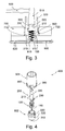
- FIG. 4 shows a three-dimensional exploded view of a contact device according to the invention.
- FIG. 5 shows a three-dimensional exploded view of a power semiconductor module with a contact device according to the invention.
- Fig. 1 shows a partial section through a disc cell (950) according to the prior art.
- This has an insulating body (954), preferably made of ceramic.
- This Isolierstoff Ari (954) forms the housing of the disc cell (950), their upper and lower cover (956, 952) are formed as metal moldings.
- a power semiconductor device (600) is arranged inside the disc cell (950).
- the one metal shaped body (956) has a recess (958).
- the gate contact is arranged.
- This is designed as a resilient wire element (962) with an insulating sheath. The insulation covers only the part of the Wire element (962), which can come into contact with the metal moldings (956).
- the first end of the wire element (962) is arranged in a recess of the insulating material body (956) provided with a metal sleeve (964) and thus electrically conductively connected thereto.
- the second end (960) of the wire element (962) rests on the gate of the power semiconductor device (600).
- the arrangement in the metal sleeve (964) and the shape of the wire element (962) results in a spring action with an introduction of force to the second end (960) of the wire element (962) in the direction of the power semiconductor component (600).
- a disadvantage of this embodiment of the disc cell (950) is that the metal shaped body (956) must have a radially outwardly running recess (958) for receiving the wire element (962). This is not cost effective to produce, nor is the assembly of the contact device can be automated.
- FIG. 2 shows a section through an embodiment of a pressure-contacted power semiconductor module (900) according to the prior art. Shown here is a metallic base plate (902), a plastic housing (908) and a plastic lid (910). On the base plate (902), a first metal shaped body (904) is subsequently arranged on an insulating layer, on which is arranged a power semiconductor component (600) and via this a second metallic molded body (908). This second metallic molded body (908) is pressurized by means of a pressure contact device (906) and thus presses the semiconductor component (600) against the first molded body (904) and this against the base plate (902). Thus, a secure electrical contact of the semiconductor device (600) to the two moldings (904, 908) and in addition a thermal contact with the base plate (902) is ensured. The two metallic moldings (904, 908) thus serve to make contact with the main connections.
- the control terminal (610) of the power semiconductor component (600) is contacted by means of a contact device.
- This contact device consists of a metallic wire element (914) which is fixed in a holding device (912) of the housing. Starting from this holding device (912), an electrically insulated wire connection (916) to an external connection is provided.
- the second metallic molded body (908) has a recess (920), in the course of which the wire element (914) is arranged and contacts the control terminal (610) there.
- the wire element (914) and its holding device (912) are designed such that the wire element (914) builds a spring force directed toward the power semiconductor device (600).
- the control terminal of the power semiconductor module (900) is designed in pressure contact technology.
- a disadvantage of this configuration of the contact device is that the pressure introduction to the power semiconductor component (600) does not occur radially symmetrically through the recess (920) in the second molded body (908).
- Another disadvantage is that the contact devices are designed differently for different power classes of the power semiconductor module (900) and, consequently, different diameters of the power semiconductor component (600). The installation effort of the contact device is also here contrary to a cost-effective production.
- a further disadvantage of the configurations of the contact devices for disc cells according to FIG. 1 and power semiconductor modules according to FIG. 2 is that the spring arm thus extends the lateral extent between the holder (964, 912) and the contact point to the control terminal (610) of the power semiconductor component (600). is very big. Under this embodiment of the resilient wire element (962, 914) suffers the contact reliability, since the homogeneity of the spring force on the production of a variety of disc cells or power semiconductor modules is given only with considerable effort.
- FIG. 3 shows a contact device according to the invention in a power semiconductor module.
- a power semiconductor device (600) with a control terminal (610) arranged centrally on the first main surface and a first and a second power connection (620) arranged on the two opposite major surfaces of the power semiconductor device (600).
- a metallic molded body (700) formed from the sandwich of two partial molded bodies is arranged. This shaped body (700) has a round central recess (710) which has an edge (720).
- the contact device itself consists of an insulating sleeve (300), consisting of a thermoplastic or preferably duroplastic plastic, a spring element (100) and a plug formed as a metal molding (200).
- the plastic sleeve (300) is used for electrical isolation of the control signal from the power connection, which is formed by the metallic molded body (700).
- the plastic sleeve (300) has two Latching lugs (360) on. These locking lugs (360) form with the serving as abutment edge (720) of the metallic molding (700) a snap-locking connection.
- a simple mounting of the contact device in the metallic molded body (700) is possible.
- the plastic sleeve (300) designed as a barrel spring contact spring (100) is arranged inside the plastic sleeve (300) designed as a barrel spring contact spring (100) is arranged. This has on its side facing the power semiconductor component (600) side facing a centrally arranged to the spring axis pin-like extension (110) with differently shaped end. This can be exemplified dull, convex or arc, as shown, be formed.
- the extension (110) penetrates the plastic sleeve (300), wherein it is formed in such a way that the spring element (100) is secured against falling out in the direction of the control connection (610).
- the extension (110) serves to make contact with the control connection (610) of the power semiconductor component (600).
- the resilient portion of the contact spring (100) is used over the life of the disc cell or the power semiconductor module constant pressure introduction and thus secure contacting of the control terminal (610).
- the metal mold part (200) which is likewise arranged in the interior of the plastic sleeve (300), serves for electrically connecting the contact spring (100) to the external control connection of the pane cell or power semiconductor component.
- the metal mold part (200) on a first pin (210) which serves to guide the metal molding (200) and extends into the inner region of the contact spring (100).
- two further pins (230) are arranged perpendicular to the first pin (210), which form a stop for the contact spring (100) and thus serve to build up pressure.
- the metal shaped part (200) For connection to a connecting cable (500), which has a plug sleeve (510), the metal shaped part (200) has a second pin (220), which is designed as a plug. Thus, the connection to an external terminal is formed.
- the contact device such that the plastic sleeve (300) is formed such that it itself has an abutment for the spring element and the power semiconductor device facing away from the spring end by means of a soldering or welding connection directly to the connection cable (500) is.
- FIG. 4 shows a three-dimensional exploded view of a contact device (400) according to the invention. Shown here are the plastic sleeve (300), the contact spring (100) and the metal mold part (200).
- the plastic sleeve (300) is in this case formed in two pieces.
- a first partial sleeve (302) forms the part of the plastic sleeve (300) which faces the power semiconductor component (600). It is designed in such a way that the contact spring (100) provided with a blunt end is secured against falling out in the direction of the control connection (610) and for this purpose has a recess (310) which is approximately 0.2 mm larger than the diameter of the pin-like extension (110) of the contact spring.
- the first partial sleeve (302) has a latching edge (320) and two recesses (330) at the upper edge, whose functions are described below.
- the second partial sleeve (304) has four further locking lugs (350) on the lugs are arranged facing inwards and find their abutment in the locking edge (320) of the first partial sleeve (302).
- both the contact spring (100) and the metal molded part (200) already written above are fixed inside the plastic sleeve (300).
- the contact spring (100) is arranged, wherein the pin-like extension (110) extends through the under recess (310) and thus fixes the contact spring (100) downwards.
- the metal shaped part (200) projects into the interior of the contact spring (100) with a first pin (210).
- the two further pins (230) formed at right angles to the first pin (210) are arranged in the recesses (330) of the first partial sleeve (302) and fixed there by connecting the two partial sleeves (302, 304). This results in a mounting unit formed from the contact spring (100), the metal mold part (200) and the two parts (302, 304) of the plastic sleeve (300).
- the contact device (400) is here an assembly unit during assembly of the power semiconductor module (800).
- the respective contact devices (400) are used for this purpose in the associated molded body (700) and engage at their latching edges (720).
- These moldings (700) are formed from a thermoset plastic, since they are not used for pressure initiation via the pressure contact device (808) but not the electrical connection, since the load connections (812) are designed here as metallic connecting lugs.
- the electrical connection between the contact device (400) to the outside is in turn formed by means of a cable (500) with plug-in sleeve (510) connected thereto.
- the plug-in sleeve (510) is arranged on the second pin (220, see Fig. 3) of the contact device (400) designed as a plug.
Abstract
Description
Es wird eine Kontakteinrichtung für den Steueranschluss von Leistungshalbleiterbauelementen in Scheibenzellen und Leistungshalbleitermodulen beschrieben. Derartige Kontakteinrichtungen sind Teil von Scheibenzellen wie sie beispielhaft bekannt sind aus Heumann, "Grundlagen der Leistungselektronik", Teubner Verlag, 6. Auflage, ISBN 3-519-06110-4, Seite 37 und von vorzugsweise druckkontaktierten Leistungshalbleitermodulen wie sie beispielhaft aus der DE 196 51 632 A1 bekannt sind.A contact device for the control connection of power semiconductor components in disk cells and power semiconductor modules is described. Such contact devices are part of disc cells as they are known by way of example from Heumann, "Basics of Power Electronics", Teubner Verlag, 6th edition, ISBN 3-519-06110-4, page 37 and preferably pressure-contacted power semiconductor modules as exemplified in DE 196 51 632 A1 are known.
Druckkontaktierte Leistungshalbleitermodule wie beispielhaft diejenigen gemäß der DE 196 51 632 A1 sind für sehr hohe Leistungsanforderungen hinsichtlich Stromtragfähigkeit und Zuverlässigkeit geeignet. Daher kommt auch dem Steueranschluss hier eine ebenso bedeutende Rolle zu wie den Leistungsanschlüssen. Druckkontaktverbindungen der Leistungsanschlüsse sind aus der Herstellung von Halbleitermodulen als Verbindungstechnik hinlänglich bekannt und vielfach bewährt. Demgegenüber gibt es für die Kontaktverbindung von Steueranschlüssen eine Vielzahl von Varianten mit unterschiedlich hohem Fertigungsaufwand und nicht direkt damit einhergehend unterschiedlich hoher Zuverlässigkeit.Pressure-contacted power semiconductor modules such as those according to DE 196 51 632 A1 are suitable for very high power requirements in terms of current carrying capacity and reliability. Therefore, the control connection plays an equally important role here as the power connections. Pressure contact connections of the power terminals are well known from the production of semiconductor modules as a connection technique and proven many times. In contrast, there are a variety of variants with different levels of manufacturing complexity and not directly associated with different levels of reliability for the contact connection of control terminals.
Bekannt sind Lötverbindungen zwischen dem Steueranschluss des Leistungshalbleiterbauelements. Ebenso sind verschiedene Arten von federbelasteten Druckkontaktierungen bekannt, denen gemeinsam ist, dass sie eine komplexe, häufig nur manuell mögliche, Herstellung bedingen und / oder deren Zuverlässigkeit ungenügend ist.Are known solder joints between the control terminal of the power semiconductor device. Likewise, various types of spring-loaded pressure contacts are known, which have in common that they require a complex, often only manually possible, production and / or their reliability is insufficient.
Der Erfindung liegt die Aufgabe zugrunde eine Kontakteinrichtung des Steueranschlusses von Leistungshalbleiterbauelementen in Scheibenzellen und Leistungshalbleitermodulen vorzustellen, die universell einsetzbar ist, einen dauerhaft sicheren elektrischen Kontakt gewährleistet und einer einfachen Montage zugänglich ist.The invention has for its object to present a contact device of the control terminal of power semiconductor devices in disc cells and power semiconductor modules, which is universally applicable, ensures a permanently secure electrical contact and a simple assembly is accessible.
Die Aufgabe wird erfindungsgemäß gelöst, durch eine Kontakteinrichtung mit den Merkmalen des Anspruchs 1. Bevorzugte Ausführungsformen sind in den Unteransprüchen beschrieben.The object is achieved by a contact device with the features of claim 1. Preferred embodiments are described in the subclaims.
Der Grundgedanke der Erfindung geht aus von einem Leistungshalbleitermodul, vorzugsweise in Druckkontaktierung mit einem oder mehreren Leistungshalbleiterbauelementen oder einer Scheibenzelle. In einer Scheibenzelle ist typischerweise nur ein Leistungshalbleiterbauelement angeordnet, allerdings gibt es Sonderformen mit einer Mehrzahl von Leistungshalbleiterbauelementen in einem Gehäuse.The basic idea of the invention is based on a power semiconductor module, preferably in pressure contact with one or more power semiconductor components or a disk cell. In a disk cell, typically only one power semiconductor device is arranged, but there are special forms with a plurality of power semiconductor devices in a housing.
Die Erfindung bezieht sich auf Leistungshalbleitermodule oder auf Scheibenzellen mit mindestens einem gesteuerten Leistungshalbleiterbauelement, wie einem Thyristor oder einem Transistor. Diese weisen einen Steueranschluss auf, der von außerhalb des Leistungshalbleitermoduls oder der Scheibenzelle mit einem Steuersignal beaufschlagt wird.The invention relates to power semiconductor modules or disk cells with at least one controlled power semiconductor device, such as a thyristor or a transistor. These have a control terminal, which is acted upon from outside the power semiconductor module or the disk cell with a control signal.
Häufig werden die Halbleiterbauelemente in Leistungshalbleitermodulen und Scheibenzellen beidseitig mit je einem flächigen Metallkörper verbunden, dessen Wärmeausdehnungskoeffizient zwischen dem Wärmeausdehnungskoeffizienten des Halbleiterbauelements und dem Wärmeausdehnungskoeffizienten einer anschließenden Kontakteinrichtung der Leistungsanschlüsse liegt, um den thermischen Stress für das Halbleiterbauelement zu verringern. Die Verbindung des Halbleiterbauelements mit den flächigen Metallkörpern, die vorzugsweise aus Molybdän bestehen, kann durch unterschiedliche Verfahren realisiert werden, beispielhaft durch Verlöten, Verkleben oder Druckkontaktierung der beiden Partner. Der flächige Metallkörper weist typischerweise eine Dicke in der Größenordnung von einigen zehntel bis einigen Millimetern auf.Frequently, the semiconductor devices in power semiconductor modules and disc cells are connected on both sides with a flat metal body, the coefficient of thermal expansion between the coefficient of thermal expansion of the semiconductor device and the coefficient of thermal expansion of a subsequent contact means of the power terminals is to reduce the thermal stress for the semiconductor device. The connection of the semiconductor component with the flat metal bodies, which preferably consist of molybdenum, can be realized by different methods, for example by soldering, gluing or pressure contacting of the two partners. The sheet metal body typically has a thickness of the order of a few tenths to a few millimeters.
Der erfindungsgemäßen Kontakteinrichtung zur Kontaktierung des Steueranschlusses des mindestens einen Leistungshalbleiterbauelements ist auf der den Haupt- und den Steueranschluss tragenden Hauptfläche ein Formkörper, beispielhaft den oben genannten flächigen Metallkörper, zugeordnet. Dieser Formkörper weist im Bereich oberhalb des Steueranschlusses eine Ausnehmung auf und diese Ausnehmung weist wiederum ein Widerlager auf.The contact device according to the invention for contacting the control terminal of the at least one power semiconductor component is assigned to the main surface and the control connection carrying main surface a molded body, for example, the above-mentioned sheet metal body. This shaped body has in the area above the control terminal on a recess and this recess in turn has an abutment.
Die Kontakteinrichtung selbst besteht aus einer Kontaktfeder mit einem stiftartigen Fortsatz an demjenigen Federende, der den Steueranschluss kontaktiert. Weiterhin weist sie eine direkt oder über ein Metallformteil gebildete Verbindung mit einem Anschlusskabel zur externen Verbindung am anderen Federende auf. Die Kontaktfeder und das optionale Metallformteil sind in einer Isolierstoffhülse angeordnet, wobei diese Isolierstoffhülse mindestens eine Rastnase aufweist die zusammen mit dem Widerlager des Formkörpers eine Schnapp- Rast- Verbindung bildet.The contact device itself consists of a contact spring with a pin-like extension at that end of the spring, which contacts the control terminal. Furthermore, it has a connection formed directly or via a metal mold part with a connection cable to the external connection at the other end of the spring. The contact spring and the optional metal molded part are arranged in an insulating sleeve, said insulating sleeve having at least one locking lug which forms a snap-locking connection together with the abutment of the molded body.
Der erfinderische Gedanke wird anhand der Ausführungsbeispiele in den Fig. 1 bis 5 näher erläutert.The inventive idea is explained in more detail with reference to the embodiments in FIGS. 1 to 5.
Fig. 1 zeigt eine Ausgestaltung einer Scheibenzelle nach dem Stand der Technik.Fig. 1 shows an embodiment of a disc cell according to the prior art.
Fig. 2 zeigt einen Schnitt durch eine Ausgestaltung eines druckkontaktierten Leistungshalbleiermoduls nach dem Stand der Technik.2 shows a section through an embodiment of a pressure-contacted power semiconductor module according to the prior art.
Fig. 3 zeigt eine erfindungsgemäße Kontakteinrichtung in einem Leistungshalbleitermodul.3 shows a contact device according to the invention in a power semiconductor module.
Fig. 4 zeigt eine dreidimensionale Explosionsdarstellung einer erfindungsgemäßen Kontakteinrichtung.4 shows a three-dimensional exploded view of a contact device according to the invention.
Fig. 5 zeigt eine dreidimensionale Explosionsdarstellung eines Leistungshalbleitermoduls mit einer erfindungsgemäßen Kontakteinrichtung.5 shows a three-dimensional exploded view of a power semiconductor module with a contact device according to the invention.
Fig. 1 zeigt einen Teilschnitt durch eine Scheibenzelle (950) gemäß dem Stand der Technik. Diese weist einen Isolierstoffkörper (954) vorzugsweise aus Keramik auf. Dieser Isolierstoffkörper (954) bildet das Gehäuse der Scheibenzelle (950), ihre obere und untere Abdeckung (956, 952) sind als Metallformkörper ausgebildet. Im Inneren der Scheibenzelle (950) ist ein Leistungshalbleiterbauelement (600) angeordnet.Fig. 1 shows a partial section through a disc cell (950) according to the prior art. This has an insulating body (954), preferably made of ceramic. This Isolierstoffkörper (954) forms the housing of the disc cell (950), their upper and lower cover (956, 952) are formed as metal moldings. Inside the disc cell (950), a power semiconductor device (600) is arranged.
In dieser Ausgestaltung der Scheibenzelle (950) weist der eine Metallformkörper (956) eine Ausnehmung (958) auf. In dieser Ausnehmung (958) ist die Gatekontakteinrichung angeordnet. Diese ist als federndes Drahtelement (962) mit einer isolierenden Umhüllung ausgebildet. Die Isolierung überdeckt ausschließlich den Teil des Drahtelements (962), der mit dem Metallformkörper (956) in Kontakt kommen kann. Das erste Ende des Drahtelements (962) ist in einer mit einer Metallhülse (964) versehenen Ausnehmung des Isolierstoffkörpers (956) angeordnet und mit dieser somit elektrisch leitend verbunden. Das zweite Ende (960) des Drahtelements (962) liegt auf dem Gateanschluss des Leistungshalbleiterbauelements (600) auf. Durch die Anordnung in der Metallhülse (964) und die Form des Drahtelements (962) ergibt sich eine Federwirkung mit einer Krafteinleitung auf das zweite Ende (960) des Drahtelements (962) in Richtung des Leistungshalbleiterbauelements (600).In this embodiment of the disc cell (950), the one metal shaped body (956) has a recess (958). In this recess (958), the gate contact is arranged. This is designed as a resilient wire element (962) with an insulating sheath. The insulation covers only the part of the Wire element (962), which can come into contact with the metal moldings (956). The first end of the wire element (962) is arranged in a recess of the insulating material body (956) provided with a metal sleeve (964) and thus electrically conductively connected thereto. The second end (960) of the wire element (962) rests on the gate of the power semiconductor device (600). The arrangement in the metal sleeve (964) and the shape of the wire element (962) results in a spring action with an introduction of force to the second end (960) of the wire element (962) in the direction of the power semiconductor component (600).
Nachteilig an dieser Ausgestaltung der Scheibenzelle (950) ist, dass der Metallformkörper (956) eine radial nach außen laufende Ausnehmung (958) zur Aufnahme des Drahtelements (962) aufweisen muss. Diese ist nicht kosteneffizient herstellbar, ebenso wenig ist die Montage der Kontakteinrichtung automatisierbar.A disadvantage of this embodiment of the disc cell (950) is that the metal shaped body (956) must have a radially outwardly running recess (958) for receiving the wire element (962). This is not cost effective to produce, nor is the assembly of the contact device can be automated.
Fig. 2 zeigt einen Schnitt durch eine Ausgestaltung eines druckkontaktierten Leistungshalbleitermoduls (900) nach dem Stand der Technik. Dargestellt ist hierbei eine metallische Grundplatte (902), eine Kunststoffgehäuse (908) und ein Kunststoffdeckel (910). Auf der Grundplatte (902) ist nachfolgend einer Isolierschicht ein erster Metallformkörper (904) angeordnet, auf diesem ist ein Leistungshalbleiterbauelement (600) und hierüber ein zweiter metallischer Formkörper (908) angeordnet. Dieser zweite metallische Formkörper (908) wird mittels einer Druckkontakteinrichtung (906) mit Druck beaufschlagt und drückt somit das Halbleiterbauelement (600) gegen den ersten Formkörper (904) und diesen gegen die Grundplatte (902). Somit ist ein sicherer elektrischer Kontakt des Halbleiterbauelements (600) zu den beiden Formkörper (904, 908) und zusätzlich ein thermischer Kontakt zur Grundplatte (902) sichergestellt. Die beiden metallischen Formkörper (904, 908) dienen somit der Kontaktierung der Hauptanschlüsse.2 shows a section through an embodiment of a pressure-contacted power semiconductor module (900) according to the prior art. Shown here is a metallic base plate (902), a plastic housing (908) and a plastic lid (910). On the base plate (902), a first metal shaped body (904) is subsequently arranged on an insulating layer, on which is arranged a power semiconductor component (600) and via this a second metallic molded body (908). This second metallic molded body (908) is pressurized by means of a pressure contact device (906) and thus presses the semiconductor component (600) against the first molded body (904) and this against the base plate (902). Thus, a secure electrical contact of the semiconductor device (600) to the two moldings (904, 908) and in addition a thermal contact with the base plate (902) is ensured. The two metallic moldings (904, 908) thus serve to make contact with the main connections.
Der Steueranschluss (610) des Leistungshalbleiterbauelements (600) wird mittels einer Kontakteinrichtung kontaktiert. Diese Kontakteinrichtung besteht aus einem metallischen Drahtelement (914), der in einer Halteeinrichtung (912) des Gehäuses fixiert ist. Von dieser Halteeinrichtung (912) ausgehend ist eine elektrisch isolierte Drahtverbindung (916) zu einem äußeren Anschluss vorgesehen. Der zweite metallische Formkörper (908) weist eine Aussparung (920) auf, in deren Verlauf das Drahtelement (914) angeordnet ist und dort den Steueranschluss (610) kontaktiert. Das Drahtelement (914)sowie dessen Halteeinrichtung (912) sind derart ausgestaltet, dass das Drahtelement (914) eine Federkraft aufbaut, die auf das Leistungshalbleiterbauelement (600) hin gerichtet ist. Somit ist auch der Steueranschluss des Leistungshalbleitermoduls (900) in Druckkontakttechnik ausgeführt.The control terminal (610) of the power semiconductor component (600) is contacted by means of a contact device. This contact device consists of a metallic wire element (914) which is fixed in a holding device (912) of the housing. Starting from this holding device (912), an electrically insulated wire connection (916) to an external connection is provided. The second metallic molded body (908) has a recess (920), in the course of which the wire element (914) is arranged and contacts the control terminal (610) there. The wire element (914) and its holding device (912) are designed such that the wire element (914) builds a spring force directed toward the power semiconductor device (600). Thus, the control terminal of the power semiconductor module (900) is designed in pressure contact technology.
Nachteilig an dieser Ausgestaltung der Kontakteinrichtung ist allerdings, dass durch die Ausnehmung (920) im zweiten Formkörper (908) die Druckeinleitung auf das Leistungshalbleiterbauelement (600) nicht radialsymmetrisch erfolgt. Weiterhin nachteilig ist, dass für verschiedene Leistungsklassen des Leistungshalbleitermoduls (900) und damit einhergehend unterschiedliche Durchmesser des Leistungshalbleiterbauelements (600) die Kontakteinrichtungen unterschiedlich ausgebildet sind. Der Montageaufwand der Kontakteinrichtung steht hier ebenfalls einer kostengünstigen Fertigung entgegen.However, a disadvantage of this configuration of the contact device is that the pressure introduction to the power semiconductor component (600) does not occur radially symmetrically through the recess (920) in the second molded body (908). Another disadvantage is that the contact devices are designed differently for different power classes of the power semiconductor module (900) and, consequently, different diameters of the power semiconductor component (600). The installation effort of the contact device is also here contrary to a cost-effective production.
Nachteilig an den Ausgestaltungen der Kontakteinrichtungen für Scheibenzellen nach Fig. 1 und Leistungshalbleitermodulen nach Fig. 2 ist weiterhin, dass der Federarm also die laterale Ausdehnung zwischen der Halterung (964, 912) und der Kontaktstelle also dem Steueranschluss (610) des Leistungshalbleiterbauelements (600) sehr groß ist. Unter dieser Ausgestaltung des federnden Drahtelements (962, 914) leidet die Kontaktsicherheit, da die Homogenität der Federkraft über die Produktion einer Vielzahl von Scheibenzellen bzw. Leistungshalbleitermodulen nur mit erheblichem Aufwand gegeben ist.A further disadvantage of the configurations of the contact devices for disc cells according to FIG. 1 and power semiconductor modules according to FIG. 2 is that the spring arm thus extends the lateral extent between the holder (964, 912) and the contact point to the control terminal (610) of the power semiconductor component (600). is very big. Under this embodiment of the resilient wire element (962, 914) suffers the contact reliability, since the homogeneity of the spring force on the production of a variety of disc cells or power semiconductor modules is given only with considerable effort.
Fig. 3 zeigt eine erfindungsgemäße Kontakteinrichtung in einem Leistungshalbleitermodul. Dargestellt ist ein Leistungshalbleiterbauelement (600) mit einem Steueranschluss (610) zentral auf dessen erster Hauptfläche angeordnet sowie einem ersten und einem zweiten Leistungsanschluss (620) angeordnet auf den beiden gegenüberliegenden Hauptflächen des Leistungshalbleiterbauelements (600). Über der ersten Hauptfläche des Leistungshalbleiterbauelements (600) ist ein metallischer Formkörper (700), gebildet aus dem Sandwich zweier Teilformkörper angeordnet. Dieser Formkörper (700) weist eine runde zentrale Ausnehmung (710) auf, die eine Kante (720) aufweist.3 shows a contact device according to the invention in a power semiconductor module. Shown is a power semiconductor device (600) with a control terminal (610) arranged centrally on the first main surface and a first and a second power connection (620) arranged on the two opposite major surfaces of the power semiconductor device (600). Over the first main surface of the power semiconductor component (600), a metallic molded body (700) formed from the sandwich of two partial molded bodies is arranged. This shaped body (700) has a round central recess (710) which has an edge (720).
Die Kontakteinrichtung selbst besteht aus einer Isolierstoffhülse (300), bestehend aus einem thermo- oder vorzugsweise duroplasten Kunststoff, einem Federelement (100) und einem als Stecker ausgebildeten Metallformteil (200). Die Kunststoffhülse (300) dient der elektrischen Isolation des Steuersignals vom Leistungsanschluss, der durch den metallischen Formkörper (700) gebildet wird. Die Kunststoffhülse (300) weist zwei Rastnasen (360) auf. Diese Rastnasen (360) bilden mit der als Widerlager dienenden Kante (720) des metallischen Formkörpers (700) eine Schnapp- Rast- Verbindung. Somit ist eine einfache Montage der Kontakteinrichtung in dem metallischen Formkörper (700) möglich.The contact device itself consists of an insulating sleeve (300), consisting of a thermoplastic or preferably duroplastic plastic, a spring element (100) and a plug formed as a metal molding (200). The plastic sleeve (300) is used for electrical isolation of the control signal from the power connection, which is formed by the metallic molded body (700). The plastic sleeve (300) has two Latching lugs (360) on. These locking lugs (360) form with the serving as abutment edge (720) of the metallic molding (700) a snap-locking connection. Thus, a simple mounting of the contact device in the metallic molded body (700) is possible.
Im Inneren der Kunststoffhülse (300) ist die als Tonnenfeder ausgebildete Kontaktfeder (100) angeordnet. Dieses weist an ihrer dem Leistungshalbleiterbauelement (600) zugewandten Seite einen zentral zur Federachse angeordneten stiftartigen Fortsatz (110) mit unterschiedlich gestaltetem Ende auf. Diese kann beispielhaft stumpf, ballig oder als Bogen, wie dargestellt, ausgebildet sein. Der Fortsatz (110) durchdringt die Kunststoffhülse (300), wobei diese derart ausgebildet ist, dass das Federelement (100) in Richtung des Steueranschlusses (610) gegen Herausfallen gesichert ist. Der Fortsatz (110) dient der Kontaktierung des Steueranschlusses (610) des Leistungshalbleiterbauelements (600). Der federnde Abschnitt der Kontaktfeder (100) dient der über die Lebensdauer der Scheibenzelle bzw. des Leistungshalbleitermoduls konstanten Druckeinleitung und damit sicheren Kontaktierung des Steueranschlusses (610).Inside the plastic sleeve (300) designed as a barrel spring contact spring (100) is arranged. This has on its side facing the power semiconductor component (600) side facing a centrally arranged to the spring axis pin-like extension (110) with differently shaped end. This can be exemplified dull, convex or arc, as shown, be formed. The extension (110) penetrates the plastic sleeve (300), wherein it is formed in such a way that the spring element (100) is secured against falling out in the direction of the control connection (610). The extension (110) serves to make contact with the control connection (610) of the power semiconductor component (600). The resilient portion of the contact spring (100) is used over the life of the disc cell or the power semiconductor module constant pressure introduction and thus secure contacting of the control terminal (610).
Das ebenfalls im Inneren der Kunststoffhülse (300) angeordnete Metallformteil (200) dient der elektrischen Verbindung der Kontaktfeder (100) mit dem externen Steueranschluss der Scheibenzelle bzw. des Leistungshalbleiterbauelements. Hierzu weist das Metallformteil (200) einen ersten Zapfen (210) auf, der zur Führung des Metallformteils (200) dient und in den Innenbereich der Kontaktfeder (100) hineinreicht. Weiterhin sind zwei weitere Zapfen (230) rechtwinkelig zum ersten Zapfen (210) angeordnet, die einen Anschlag für die Kontaktfeder (100) bilden und somit zum Druckaufbau dienen.The metal mold part (200), which is likewise arranged in the interior of the plastic sleeve (300), serves for electrically connecting the contact spring (100) to the external control connection of the pane cell or power semiconductor component. For this purpose, the metal mold part (200) on a first pin (210) which serves to guide the metal molding (200) and extends into the inner region of the contact spring (100). Furthermore, two further pins (230) are arranged perpendicular to the first pin (210), which form a stop for the contact spring (100) and thus serve to build up pressure.
Zur Verbindung mit einem Anschlusskabel (500), das eine Steckerhülse (510) aufweist, weist das Metallformteil (200) einen zweiten Zapfen (220) auf, der als Stecker ausgebildet ist. Somit wird die Verbindung zu einem externen Anschluss gebildet.For connection to a connecting cable (500), which has a plug sleeve (510), the metal shaped part (200) has a second pin (220), which is designed as a plug. Thus, the connection to an external terminal is formed.
Alternativ und kostengünstiger ist eine Ausgestaltung der Kontakteinrichtung derart, dass die Kunststoffhülse (300) derart ausgebildet ist, dass sie selbst ein Widerlager für das Federelement aufweist und das dem Leistungshalbleiterbauelement abgewandte Federende mittels einer Löt-, oder Schweißverbindung direkt mit dem Anschlusskabel (500) verbunden ist.Alternatively and cost is an embodiment of the contact device such that the plastic sleeve (300) is formed such that it itself has an abutment for the spring element and the power semiconductor device facing away from the spring end by means of a soldering or welding connection directly to the connection cable (500) is.
Fig. 4 zeigt eine dreidimensionale Explosionsdarstellung einer erfindungsgemäßen Kontakteinrichtung (400). Dargestellt sind hier die Kunststoffhülse (300), die Kontaktfeder (100) und das Metallformteil (200). Die Kunststoffhülse (300) ist hierbei zweistückig ausgebildet. Eine erste Teilhülse (302) bildet den Teil der Kunststoffhülse (300), der dem Leistungshalbleiterbauelement (600) zugewandt ist. Sie ist derart ausgebildet dass die mit einem stumpfen Ende versehene Kontaktfeder (100) in Richtung des Steueranschlusse (610) gegen Herausfallen gesichert ist und weist hierzu eine Ausnehmung (310) auf, die ca. 0,2mm größer ist als der Durchmesser des stiftartigen Fortsatzes (110) der Kontaktfeder. Weiterhin weist die erste Teilhülse (302) eine Rastkante (320) sowie zwei Ausnehmungen (330) am oberen Rand auf, deren Funktionen unten beschrieben werden.4 shows a three-dimensional exploded view of a contact device (400) according to the invention. Shown here are the plastic sleeve (300), the contact spring (100) and the metal mold part (200). The plastic sleeve (300) is in this case formed in two pieces. A first partial sleeve (302) forms the part of the plastic sleeve (300) which faces the power semiconductor component (600). It is designed in such a way that the contact spring (100) provided with a blunt end is secured against falling out in the direction of the control connection (610) and for this purpose has a recess (310) which is approximately 0.2 mm larger than the diameter of the pin-like extension (110) of the contact spring. Furthermore, the first partial sleeve (302) has a latching edge (320) and two recesses (330) at the upper edge, whose functions are described below.
Ebenso dargestellt ist eine zweite Teilhülse (304) mit vier Rastnasen (360), wobei die Nasen nach außen gewandt angeordnet sind, zur Schnapp- Rast- Verbindung mit dem metallischen Formteil (siehe Fig. 3, 700) an dessen zugeordnetem Widerlager (vgl. Fig. 2, 710). Weiterhin weist die zweite Teilhülse (304) vier weitere Rastnasen (350) auf deren Nasen nach innen gewandt angeordnet sind und ihr Widerlager in der Rastkante (320) der ersten Teilhülse (302) finden. Mittels dieser zweiten Schnapp- Rast- Verbindung werden die beiden Teilhülsen (302, 304) aneinander fixiert.Also shown is a second sub-sleeve (304) with four locking lugs (360), wherein the lugs are arranged facing outward, the snap-locking connection with the metallic molding (see Fig. 3, 700) at its associated abutment (see. Fig. 2, 710). Furthermore, the second partial sleeve (304) has four further locking lugs (350) on the lugs are arranged facing inwards and find their abutment in the locking edge (320) of the first partial sleeve (302). By means of this second snap-locking connection, the two sub-sleeves (302, 304) are fixed to each other.
Bei der genannten Fixierung der beiden Teilhülsen (302, 304) zu einer Kunststoffhülse (300) wird weiterhin sowohl die Kontaktfeder (100) als auch das bereits oben geschriebene Metallformteil (200) im Inneren der Kunststoffhülse (300) fixiert. Hierzu dienen die beiden Ausnehmungen (330) am oberen Rand der ersten Teilhülse (302). In dieser ersten Teilhülse (302) ist die Kontaktfeder (100) angeordnet, wobei der stiftartige Fortsatz (110) durch die unter Ausnehmung (310) hindurchreicht und somit die Kontaktfeder (100) nach unten fixiert. Am oberen Federende ragt das Metallformteil (200) mit einem ersten Zapfen (210) ins Innere der Kontaktfeder (100) hinein. Die beiden rechtwinkelig zu dem ersten Zapfen (210) ausgebildeten weiteren Zapfen (230) werden in den Ausnehmungen (330) der ersten Teilhülse (302) angeordnet und durch das Verbinden der beiden Teilhülsen (302, 304) dort fixiert. Somit ergibt sich eine Montageeinheit gebildet aus der Kontaktfeder (100), dem Metallformteil (200) und die beiden Teilen (302, 304) der Kunststoffhülse (300).In the above-mentioned fixation of the two sub-sleeves (302, 304) to form a plastic sleeve (300), both the contact spring (100) and the metal molded part (200) already written above are fixed inside the plastic sleeve (300). For this purpose, the two recesses (330) at the upper edge of the first partial sleeve (302). In this first partial sleeve (302), the contact spring (100) is arranged, wherein the pin-like extension (110) extends through the under recess (310) and thus fixes the contact spring (100) downwards. At the upper end of the spring, the metal shaped part (200) projects into the interior of the contact spring (100) with a first pin (210). The two further pins (230) formed at right angles to the first pin (210) are arranged in the recesses (330) of the first partial sleeve (302) and fixed there by connecting the two partial sleeves (302, 304). This results in a mounting unit formed from the contact spring (100), the metal mold part (200) and the two parts (302, 304) of the plastic sleeve (300).
Fig. 5 zeigt eine dreidimensionale Explosionsdarstellung eines Leistungshalbleitermoduls (800) mit einer erfindungsgemäßen Kontakteinrichtung (400). Dargestellt ist ein Leistungshalbleitermodul (800) mit zwei Thyrisoren (600) aufgebaut in Druckkontakttechnik. Auf einer Grundplatte (802) sind in geeigneter Weise angeordnet:
- Isolationsmaterial zur elektrischen Isolation der Strom führenden Teile des Leistungshalbleitermoduls (800) von der Grundplatte (802);
- die beiden Thyristoren (600) mit geeigneten elektrischen Verbindungselementen (812);
- zwei Formkörper (700) zur Aufnahme der Kontakteinrichtung und zur Einleitung des Drucks aus
- einer Druckkontakteinrichtung (808) vergleichbar derer in Fig. 2 beschriebenen und
- ein Gehäuse (804) mit Deckel (810).
- Insulating material for electrically insulating the current carrying parts of the power semiconductor module (800) from the base plate (802);
- the two thyristors (600) with suitable electrical connection elements (812);
- two moldings (700) for receiving the contact device and to initiate the pressure
- a pressure contact device (808) comparable to those described in Fig. 2 and
- a housing (804) with cover (810).
Die erfindungsgemäße Kontakteinrichtung (400) ist hier eine Montageeinheit beim Zusammenbau des Leistungshalbleitermoduls (800). Die jeweiligen Kontakteinrichtungen (400) werden hierzu in die zugeordneten Formkörper (700) eingesetzt und rasten an deren Rastkanten (720) ein. Diese Formkörper (700) sind aus einem duroplasten Kunststoff gebildet, da sie nur der Druckeinleitung über die Druckkontakteinrichtung (808) nicht aber der elektrischen Verbindung dienen, da die Lastanschlüsse (812) sind hier als metallische Anschlusslaschen ausgeführt. Die elektrische Verbindung zwischen der Kontakteinrichtung (400) nach außen wird wiederum mittels eines Kabels (500) mit damit verbundener Steckhülse (510) gebildet. Hierzu ist die Steckhülse (510) auf dem als Stecker ausgebildeten zweiten Zapfen (220, vgl. Fig. 3) der Kontakteinrichtung (400) angeordnet.The contact device (400) according to the invention is here an assembly unit during assembly of the power semiconductor module (800). The respective contact devices (400) are used for this purpose in the associated molded body (700) and engage at their latching edges (720). These moldings (700) are formed from a thermoset plastic, since they are not used for pressure initiation via the pressure contact device (808) but not the electrical connection, since the load connections (812) are designed here as metallic connecting lugs. The electrical connection between the contact device (400) to the outside is in turn formed by means of a cable (500) with plug-in sleeve (510) connected thereto. For this purpose, the plug-in sleeve (510) is arranged on the second pin (220, see Fig. 3) of the contact device (400) designed as a plug.
Claims (9)
wobei die Kontakteinrichtung (400) besteht
aus einer Kontaktfeder (100) mit einem stiftartigen Fortsatz (110) an demjenigen Federende, der den Steueranschluss (610) kontaktiert, und mit einer direkt oder über ein Metallformteil (200) gebildeten Verbindung mit einem Anschlusskabel (500) zur externen Verbindung am anderen Federende und
aus einer Isolierstoffhülse (300) mit darin angeordneter Kontaktfeder (100), wobei diese Isolierstoffhülse (300) mindestens eine Rastnase (360) aufweist die zusammen mit dem Widerlager (720) des Formkörpers (700) eine Schnapp- Rast- Verbindung bildet.Contact device (400) for contacting the control terminal (610) of a power semiconductor device (600) in a power semiconductor module (800) or a disk cell wherein above the power semiconductor device (600) a molded body (700) is arranged, in the region of the control terminal (610) has a recess (710) and this recess (710) has an abutment (720),
wherein the contact means (400) consists
of a contact spring (100) with a pin-like extension (110) at that spring end which contacts the control terminal (610) and with a connection formed directly or via a metal mold part (200) to a connection cable (500) for external connection at the other spring end and
of an insulating sleeve (300) with arranged therein contact spring (100), said insulating sleeve (300) has at least one latching lug (360) which forms a snap-locking connection together with the abutment (720) of the shaped body (700).
wobei die Isolierstoffhülse (300) zweistückig ausgebildet ist und die beiden Teile (302, 304) über eine Schnapp- Rast- Verbindung zueinander angeordnet sind.Contact device according to claim 1,
wherein the insulating sleeve (300) is formed in two pieces and the two parts (302, 304) via a snap-locking connection to each other are arranged.
wobei die Kontaktfeder (100) im Wesentlichen als Tonnenfeder ausgebildet ist.Contact device according to claim 1,
wherein the contact spring (100) is formed substantially as a barrel spring.
wobei das Metallformteil (200) einen ersten Zapfen (210) aufweist, der in den Innenbereich der Kontaktfeder (100) hineinreicht und einen zweiten Zapfen (220) aufweist, der als Stecker ausgebildet ist und mit dem Anschlusskabel (500), das eine Steckerhülse (510) aufweist, mittels einer daraus gebildeten Steckverbindung verbunden ist.Contact device according to claim 2 and 3,
wherein the metal mold part (200) has a first pin (210) which extends into the inner region of the contact spring (100) and has a second pin (220) which is designed as a plug and with the connecting cable (500) which has a plug sleeve ( 510) is connected by means of a plug connection formed therefrom.
wobei das Metallformteil (200) weitere Zapfen (230) rechtwinkelig zu dem ersten (210) und zweiten Zapfen (220) angeordnet aufweist, die mittels der beiden Teile (301, 302) der Isolierstoffhülse (300) angeordnet sind und das Metallformteil (200) hierdurch im Inneren der Isolierstoffhülse (300) gehalten wird.Contact device according to claim 4,
wherein the metal mold part (200) has further pins (230) arranged at right angles to the first (210) and second pin (220), which are arranged by means of the two parts (301, 302) of the insulating sleeve (300) and the metal mold part (200). thereby held inside the insulating sleeve (300).
wobei der zweite, dem Steueranschluss (610) zugewandete Teil (310) der Isolierstoffhülse (300) derart ausgebildet ist, dass die Kontaktfeder (100) in Richtung des Steueranschlusse (610) gegen Herausfallen gesichert ist.Contact device according to claim 2,
wherein the second, the control terminal (610) facing part (310) of the insulating sleeve (300) is formed such that the contact spring (100) in the direction of the control terminal (610) is secured against falling out.
wobei die Kontaktfeder (100), das Metallformteil (200) und die beiden Teile (302, 304) der Isolierstoffhülse (300) eine Montageeinheit bilden.Contact device according to claim 5 and 6,
wherein the contact spring (100), the metal mold part (200) and the two parts (302, 304) of the insulating sleeve (300) form a mounting unit.
wobei die Kontaktfeder (100) mittels einer Schweiß- oder Lötverbindung mit dem Anschlusskabel (500) verbunden ist.Contact device according to claim,
wherein the contact spring (100) is connected to the connection cable (500) by means of a weld or solder connection.
wobei der Formkörper (700) einstückig oder mehrstückig ausgebildet ist, aus einem metallischen Werkstoff besteht und einen Hauptanschluss (620) des Leistungshalbleiterbauelements (600) elektrisch kontaktiert.Contact device according to claim 1,
wherein the molded body (700) is integrally or multi-piece, consists of a metallic material and a main terminal (620) of the power semiconductor device (600) electrically contacted.
Priority Applications (1)
| Application Number | Priority Date | Filing Date | Title |
|---|---|---|---|
| PL05017563T PL1648029T3 (en) | 2004-10-16 | 2005-08-12 | Contact device for power semiconductor modules and disc-shaped semiconductor cells |
Applications Claiming Priority (1)
| Application Number | Priority Date | Filing Date | Title |
|---|---|---|---|
| DE200410050588 DE102004050588B4 (en) | 2004-10-16 | 2004-10-16 | Arrangement with a power semiconductor component and with a contact device |
Publications (3)
| Publication Number | Publication Date |
|---|---|
| EP1648029A2 true EP1648029A2 (en) | 2006-04-19 |
| EP1648029A3 EP1648029A3 (en) | 2006-09-13 |
| EP1648029B1 EP1648029B1 (en) | 2008-07-02 |
Family
ID=35502719
Family Applications (1)
| Application Number | Title | Priority Date | Filing Date |
|---|---|---|---|
| EP20050017563 Active EP1648029B1 (en) | 2004-10-16 | 2005-08-12 | Contact device for power semiconductor modules and disc-shaped semiconductor cells |
Country Status (9)
| Country | Link |
|---|---|
| US (1) | US7396261B2 (en) |
| EP (1) | EP1648029B1 (en) |
| JP (1) | JP5392966B2 (en) |
| CN (1) | CN100442493C (en) |
| AT (1) | ATE400061T1 (en) |
| DE (2) | DE102004050588B4 (en) |
| DK (1) | DK1648029T3 (en) |
| ES (1) | ES2309627T3 (en) |
| PL (1) | PL1648029T3 (en) |
Cited By (5)
| Publication number | Priority date | Publication date | Assignee | Title |
|---|---|---|---|---|
| DE102006006421A1 (en) * | 2006-02-13 | 2007-08-23 | Semikron Elektronik Gmbh & Co. Kg | Power semiconductor module has substrate with insulating material body, where connection element is formed as contact spring with two contact mechanism and springy section |
| EP1933380A2 (en) * | 2006-12-13 | 2008-06-18 | SEMIKRON Elektronik GmbH & Co. KG | Power semiconductor module with contact springs |
| DE102007010883A1 (en) * | 2007-03-06 | 2008-09-18 | Infineon Technologies Ag | Power semiconductor device and method for its production |
| EP1933379A3 (en) * | 2006-12-13 | 2009-01-14 | SEMIKRON Elektronik GmbH & Co. KG | Power semiconductor module with contact springs |
| WO2013157616A1 (en) * | 2012-04-19 | 2013-10-24 | Yazaki Corporation | Substrate connector |
Families Citing this family (15)
| Publication number | Priority date | Publication date | Assignee | Title |
|---|---|---|---|---|
| US7640267B2 (en) * | 2002-11-20 | 2009-12-29 | Radar Networks, Inc. | Methods and systems for managing entities in a computing device using semantic objects |
| DE102004058946B4 (en) * | 2004-12-08 | 2009-06-18 | Semikron Elektronik Gmbh & Co. Kg | Power semiconductor module with auxiliary connection |
| DE102005055713B4 (en) * | 2005-11-23 | 2011-11-17 | Semikron Elektronik Gmbh & Co. Kg | Power semiconductor module with connection elements |
| DE102006034964B3 (en) | 2006-07-28 | 2007-09-06 | Semikron Elektronik Gmbh & Co. Kg | Arrangement has power semiconductor element in power semiconductor module or disc cell, where shaped body is arranged with one cut above element, where contact device is for auxiliary or control connection contact of element |
| CN201000993Y (en) * | 2006-12-18 | 2008-01-02 | 富士康(昆山)电脑接插件有限公司 | Electrical connector |
| JP4900165B2 (en) * | 2007-09-27 | 2012-03-21 | 三菱電機株式会社 | Power semiconductor module |
| DE102008058189A1 (en) | 2008-11-20 | 2010-07-22 | Semikron Elektronik Gmbh & Co. Kg | Moisture-proof power semiconductor module with centering device |
| DE102009022659B4 (en) | 2009-05-26 | 2012-01-19 | Semikron Elektronik Gmbh & Co. Kg | Contact device for a power semiconductor module |
| DE102009024421B3 (en) * | 2009-06-09 | 2010-07-08 | Semikron Elektronik Gmbh & Co. Kg | Control terminal contact device for a power semiconductor component |
| DE102010035980B4 (en) * | 2010-09-01 | 2014-03-20 | Semikron Elektronik Gmbh & Co. Kg | Connection device for a power semiconductor module |
| US20140115891A1 (en) * | 2012-10-25 | 2014-05-01 | Po-Kai Hsu | Connector terminal preparation method |
| US8651900B1 (en) * | 2012-10-25 | 2014-02-18 | Po-Kai Hsu | Connector terminal |
| JP6877251B2 (en) * | 2017-06-09 | 2021-05-26 | 三菱電機株式会社 | Semiconductor devices for electric power |
| CN111681995B (en) * | 2020-04-29 | 2022-09-09 | 株洲中车时代半导体有限公司 | Thyristor element, thyristor element assembly structure and soft starter |
| US20230116532A1 (en) * | 2021-10-13 | 2023-04-13 | Eaton Intelligent Power Limited | Connector packages for fastenerless circuit coupling |
Citations (9)
| Publication number | Priority date | Publication date | Assignee | Title |
|---|---|---|---|---|
| GB1031233A (en) * | 1963-06-24 | 1966-06-02 | Standard Telephones Cables Ltd | Electrical semi-conductor device |
| GB1078342A (en) * | 1965-02-23 | 1967-08-09 | Westinghouse Brake & Signal | Semi-conductor device and manufacture thereof |
| DE1564567A1 (en) * | 1966-04-16 | 1969-09-25 | Siemens Ag | Semiconductor device |
| US4263607A (en) * | 1979-03-06 | 1981-04-21 | Alsthom-Atlantique | Snap fit support housing for a semiconductor power wafer |
| DE4227063A1 (en) * | 1992-08-15 | 1994-02-17 | Abb Research Ltd | High-performance semiconductor component that can be switched off |
| DE19651632A1 (en) * | 1996-12-12 | 1998-06-18 | Semikron Elektronik Gmbh | Power semiconductor module with pressure contacted power semiconductor element for current rectifiers |
| DE10017319A1 (en) * | 2000-04-10 | 2001-10-25 | 2 E Rolf Hiller Gmbh | Electrical connector for electronic circuit board, has plug with pins that engage conductor tracks on circuit board |
| EP1291914A1 (en) * | 2001-09-10 | 2003-03-12 | ABB Schweiz AG | Pressure-contactable power semiconductor module |
| DE10231219C1 (en) * | 2002-07-11 | 2003-05-22 | Semikron Elektronik Gmbh | Semiconductor relay has ceramic substrate carrying semiconductor elements, 2-part housing enclosing connection elements, heat sink base and control device |
Family Cites Families (12)
| Publication number | Priority date | Publication date | Assignee | Title |
|---|---|---|---|---|
| US3448352A (en) * | 1966-07-26 | 1969-06-03 | Westinghouse Electric Corp | Multiple electrical contact assembly for compression bonded electrical devices |
| US3457988A (en) * | 1967-05-15 | 1969-07-29 | Westinghouse Electric Corp | Integral heat sink for semiconductor devices |
| US3513361A (en) * | 1968-05-09 | 1970-05-19 | Westinghouse Electric Corp | Flat package electrical device |
| DE9113930U1 (en) * | 1991-11-08 | 1992-02-13 | Aerzener Maschinenfabrik Gmbh, 3258 Aerzen, De | |
| JP3000809B2 (en) * | 1993-01-08 | 2000-01-17 | 富士電機株式会社 | Semiconductor device |
| US5631959A (en) * | 1995-05-01 | 1997-05-20 | Lucent Technologies Inc. | Method and apparatus for protecting circuitry accessible through metallic contacts from static discharge damage |
| DE19651623A1 (en) * | 1996-12-12 | 1998-06-18 | Zunhammer Sebastian Dipl Ing F | Vehicle for transporting liquid manure |
| CN1257209A (en) * | 1998-11-17 | 2000-06-21 | 埃皮技术公司 | Small interval contactor |
| US6155846A (en) * | 2000-01-03 | 2000-12-05 | Motorola, Inc. | Electrical contactor assembly |
| CN2660716Y (en) * | 2003-09-23 | 2004-12-01 | 富士康(昆山)电脑接插件有限公司 | Electrical connector |
| TW200536211A (en) * | 2004-04-16 | 2005-11-01 | Advanced Connection Tech Inc | Electric connector |
| CN200941348Y (en) * | 2006-08-18 | 2007-08-29 | 富士康(昆山)电脑接插件有限公司 | Switch |
-
2004
- 2004-10-16 DE DE200410050588 patent/DE102004050588B4/en active Active
-
2005
- 2005-08-12 EP EP20050017563 patent/EP1648029B1/en active Active
- 2005-08-12 PL PL05017563T patent/PL1648029T3/en unknown
- 2005-08-12 DK DK05017563T patent/DK1648029T3/en active
- 2005-08-12 ES ES05017563T patent/ES2309627T3/en active Active
- 2005-08-12 DE DE200550004565 patent/DE502005004565D1/en active Active
- 2005-08-12 AT AT05017563T patent/ATE400061T1/en active
- 2005-08-22 JP JP2005239709A patent/JP5392966B2/en active Active
- 2005-10-14 CN CNB2005101136635A patent/CN100442493C/en active Active
- 2005-10-17 US US11/252,338 patent/US7396261B2/en active Active
Patent Citations (9)
| Publication number | Priority date | Publication date | Assignee | Title |
|---|---|---|---|---|
| GB1031233A (en) * | 1963-06-24 | 1966-06-02 | Standard Telephones Cables Ltd | Electrical semi-conductor device |
| GB1078342A (en) * | 1965-02-23 | 1967-08-09 | Westinghouse Brake & Signal | Semi-conductor device and manufacture thereof |
| DE1564567A1 (en) * | 1966-04-16 | 1969-09-25 | Siemens Ag | Semiconductor device |
| US4263607A (en) * | 1979-03-06 | 1981-04-21 | Alsthom-Atlantique | Snap fit support housing for a semiconductor power wafer |
| DE4227063A1 (en) * | 1992-08-15 | 1994-02-17 | Abb Research Ltd | High-performance semiconductor component that can be switched off |
| DE19651632A1 (en) * | 1996-12-12 | 1998-06-18 | Semikron Elektronik Gmbh | Power semiconductor module with pressure contacted power semiconductor element for current rectifiers |
| DE10017319A1 (en) * | 2000-04-10 | 2001-10-25 | 2 E Rolf Hiller Gmbh | Electrical connector for electronic circuit board, has plug with pins that engage conductor tracks on circuit board |
| EP1291914A1 (en) * | 2001-09-10 | 2003-03-12 | ABB Schweiz AG | Pressure-contactable power semiconductor module |
| DE10231219C1 (en) * | 2002-07-11 | 2003-05-22 | Semikron Elektronik Gmbh | Semiconductor relay has ceramic substrate carrying semiconductor elements, 2-part housing enclosing connection elements, heat sink base and control device |
Cited By (8)
| Publication number | Priority date | Publication date | Assignee | Title |
|---|---|---|---|---|
| DE102006006421A1 (en) * | 2006-02-13 | 2007-08-23 | Semikron Elektronik Gmbh & Co. Kg | Power semiconductor module has substrate with insulating material body, where connection element is formed as contact spring with two contact mechanism and springy section |
| DE102006006421B4 (en) * | 2006-02-13 | 2014-09-11 | Semikron Elektronik Gmbh & Co. Kg | The power semiconductor module |
| EP1933380A2 (en) * | 2006-12-13 | 2008-06-18 | SEMIKRON Elektronik GmbH & Co. KG | Power semiconductor module with contact springs |
| EP1933379A3 (en) * | 2006-12-13 | 2009-01-14 | SEMIKRON Elektronik GmbH & Co. KG | Power semiconductor module with contact springs |
| EP1933380A3 (en) * | 2006-12-13 | 2009-01-28 | SEMIKRON Elektronik GmbH & Co. KG | Power semiconductor module with contact springs |
| DE102007010883A1 (en) * | 2007-03-06 | 2008-09-18 | Infineon Technologies Ag | Power semiconductor device and method for its production |
| WO2013157616A1 (en) * | 2012-04-19 | 2013-10-24 | Yazaki Corporation | Substrate connector |
| US9270044B2 (en) | 2012-04-19 | 2016-02-23 | Yazaki Corporation | Substrate connector |
Also Published As
| Publication number | Publication date |
|---|---|
| JP5392966B2 (en) | 2014-01-22 |
| DE502005004565D1 (en) | 2008-08-14 |
| US7396261B2 (en) | 2008-07-08 |
| CN100442493C (en) | 2008-12-10 |
| US20060154527A1 (en) | 2006-07-13 |
| JP2006114883A (en) | 2006-04-27 |
| ATE400061T1 (en) | 2008-07-15 |
| EP1648029B1 (en) | 2008-07-02 |
| PL1648029T3 (en) | 2008-12-31 |
| DE102004050588B4 (en) | 2009-05-20 |
| CN1763940A (en) | 2006-04-26 |
| EP1648029A3 (en) | 2006-09-13 |
| ES2309627T3 (en) | 2008-12-16 |
| DK1648029T3 (en) | 2008-10-20 |
| DE102004050588A1 (en) | 2006-04-20 |
Similar Documents
| Publication | Publication Date | Title |
|---|---|---|
| EP1648029B1 (en) | Contact device for power semiconductor modules and disc-shaped semiconductor cells | |
| DE102009037257B4 (en) | Power semiconductor module with circuit carrier and load connection element and manufacturing method thereof | |
| EP1844526B1 (en) | Arrangement for generating an electrical flow of current through carbon fibers | |
| DE102009055882A1 (en) | Power semiconductor device | |
| EP1883108B1 (en) | Arangement with a power semiconductor device and a contact device | |
| EP1791178B1 (en) | Pressure contact type power semiconductor module | |
| EP2532051B1 (en) | Contact-making and connection arrangement on the basis of film conductors introduced in a housing | |
| DE102008057832A1 (en) | Power semiconductor module with preloaded auxiliary contact spring | |
| EP3262717A1 (en) | Plug-type connection for an electrical connection | |
| DE202015106042U1 (en) | circuit board | |
| EP3770959A1 (en) | Connection method for power modules with intermediate circuit busbar | |
| DE102017125505A1 (en) | Socket for printed circuit boards | |
| EP2305010B1 (en) | Electrical circuit arrangement | |
| EP3017511B1 (en) | Connecting device for connecting electrical lines to electrical contacts | |
| DE102010012331A1 (en) | Circuit configuration i.e. capacitor module, for e.g. electrolytic capacitor, for storing electrical power in electrical drive of circuit board, has spacing holder assembly longer than electrical components in extending direction | |
| EP3292592B1 (en) | Battery terminal and method for producing a battery terminal | |
| EP2343780A1 (en) | Semiconductor circuit assembly | |
| DE102016209604A1 (en) | Press-fit terminal, semiconductor device, power conversion device and method of making a press-fit terminal | |
| WO2013017473A2 (en) | Electronics arrangement | |
| DE10129840B4 (en) | Electric device | |
| EP3499563A1 (en) | Semiconductor power module and method for assembling a semiconductor power module in a force-fitting manner | |
| EP2425498B1 (en) | Interconnect system for a printed circuit board | |
| EP3192155A1 (en) | Electric motor having smd components and associated connection component | |
| EP3039950A1 (en) | Novel connection of a flexible circuit board to a control unit housing | |
| WO2022242987A1 (en) | Electric arrangement with a choke coil |
Legal Events
| Date | Code | Title | Description |
|---|---|---|---|
| PUAI | Public reference made under article 153(3) epc to a published international application that has entered the european phase |
Free format text: ORIGINAL CODE: 0009012 |
|
| AK | Designated contracting states |
Kind code of ref document: A2 Designated state(s): AT BE BG CH CY CZ DE DK EE ES FI FR GB GR HU IE IS IT LI LT LU LV MC NL PL PT RO SE SI SK TR |
|
| AX | Request for extension of the european patent |
Extension state: AL BA HR MK YU |
|
| PUAL | Search report despatched |
Free format text: ORIGINAL CODE: 0009013 |
|
| AK | Designated contracting states |
Kind code of ref document: A3 Designated state(s): AT BE BG CH CY CZ DE DK EE ES FI FR GB GR HU IE IS IT LI LT LU LV MC NL PL PT RO SE SI SK TR |
|
| AX | Request for extension of the european patent |
Extension state: AL BA HR MK YU |
|
| 17P | Request for examination filed |
Effective date: 20060821 |
|
| 17Q | First examination report despatched |
Effective date: 20061103 |
|
| AKX | Designation fees paid |
Designated state(s): AT BE BG CH CY CZ DE DK EE ES FI FR GB GR HU IE IS IT LI LT LU LV MC NL PL PT RO SE SI SK TR |
|
| GRAP | Despatch of communication of intention to grant a patent |
Free format text: ORIGINAL CODE: EPIDOSNIGR1 |
|
| RTI1 | Title (correction) |
Free format text: CONTACT DEVICE FOR POWER SEMICONDUCTOR MODULES AND DISC-SHAPED SEMICONDUCTOR CELLS |
|
| GRAS | Grant fee paid |
Free format text: ORIGINAL CODE: EPIDOSNIGR3 |
|
| GRAA | (expected) grant |
Free format text: ORIGINAL CODE: 0009210 |
|
| AK | Designated contracting states |
Kind code of ref document: B1 Designated state(s): AT BE BG CH CY CZ DE DK EE ES FI FR GB GR HU IE IS IT LI LT LU LV MC NL PL PT RO SE SI SK TR |
|
| REG | Reference to a national code |
Ref country code: GB Ref legal event code: FG4D Free format text: NOT ENGLISH |
|
| REG | Reference to a national code |
Ref country code: CH Ref legal event code: EP |
|
| REF | Corresponds to: |
Ref document number: 502005004565 Country of ref document: DE Date of ref document: 20080814 Kind code of ref document: P |
|
| REG | Reference to a national code |
Ref country code: CH Ref legal event code: NV Representative=s name: BRAUNPAT BRAUN EDER AG |
|
| REG | Reference to a national code |
Ref country code: IE Ref legal event code: FG4D Free format text: LANGUAGE OF EP DOCUMENT: GERMAN |
|
| REG | Reference to a national code |
Ref country code: SE Ref legal event code: TRGR |
|
| PG25 | Lapsed in a contracting state [announced via postgrant information from national office to epo] |
Ref country code: SI Free format text: LAPSE BECAUSE OF FAILURE TO SUBMIT A TRANSLATION OF THE DESCRIPTION OR TO PAY THE FEE WITHIN THE PRESCRIBED TIME-LIMIT Effective date: 20080702 |
|
| REG | Reference to a national code |
Ref country code: ES Ref legal event code: FG2A Ref document number: 2309627 Country of ref document: ES Kind code of ref document: T3 |
|
| REG | Reference to a national code |
Ref country code: PL Ref legal event code: T3 |
|
| PG25 | Lapsed in a contracting state [announced via postgrant information from national office to epo] |
Ref country code: PT Free format text: LAPSE BECAUSE OF FAILURE TO SUBMIT A TRANSLATION OF THE DESCRIPTION OR TO PAY THE FEE WITHIN THE PRESCRIBED TIME-LIMIT Effective date: 20081202 Ref country code: LT Free format text: LAPSE BECAUSE OF FAILURE TO SUBMIT A TRANSLATION OF THE DESCRIPTION OR TO PAY THE FEE WITHIN THE PRESCRIBED TIME-LIMIT Effective date: 20080702 Ref country code: IS Free format text: LAPSE BECAUSE OF FAILURE TO SUBMIT A TRANSLATION OF THE DESCRIPTION OR TO PAY THE FEE WITHIN THE PRESCRIBED TIME-LIMIT Effective date: 20081102 |
|
| REG | Reference to a national code |
Ref country code: IE Ref legal event code: FD4D |
|
| PG25 | Lapsed in a contracting state [announced via postgrant information from national office to epo] |
Ref country code: LV Free format text: LAPSE BECAUSE OF FAILURE TO SUBMIT A TRANSLATION OF THE DESCRIPTION OR TO PAY THE FEE WITHIN THE PRESCRIBED TIME-LIMIT Effective date: 20080702 Ref country code: BG Free format text: LAPSE BECAUSE OF FAILURE TO SUBMIT A TRANSLATION OF THE DESCRIPTION OR TO PAY THE FEE WITHIN THE PRESCRIBED TIME-LIMIT Effective date: 20081002 |
|
| PG25 | Lapsed in a contracting state [announced via postgrant information from national office to epo] |
Ref country code: MC Free format text: LAPSE BECAUSE OF NON-PAYMENT OF DUE FEES Effective date: 20080831 |
|
| PG25 | Lapsed in a contracting state [announced via postgrant information from national office to epo] |
Ref country code: IE Free format text: LAPSE BECAUSE OF FAILURE TO SUBMIT A TRANSLATION OF THE DESCRIPTION OR TO PAY THE FEE WITHIN THE PRESCRIBED TIME-LIMIT Effective date: 20080702 Ref country code: EE Free format text: LAPSE BECAUSE OF FAILURE TO SUBMIT A TRANSLATION OF THE DESCRIPTION OR TO PAY THE FEE WITHIN THE PRESCRIBED TIME-LIMIT Effective date: 20080702 |
|
| PLBE | No opposition filed within time limit |
Free format text: ORIGINAL CODE: 0009261 |
|
| STAA | Information on the status of an ep patent application or granted ep patent |
Free format text: STATUS: NO OPPOSITION FILED WITHIN TIME LIMIT |
|
| PG25 | Lapsed in a contracting state [announced via postgrant information from national office to epo] |
Ref country code: CZ Free format text: LAPSE BECAUSE OF FAILURE TO SUBMIT A TRANSLATION OF THE DESCRIPTION OR TO PAY THE FEE WITHIN THE PRESCRIBED TIME-LIMIT Effective date: 20080702 Ref country code: RO Free format text: LAPSE BECAUSE OF FAILURE TO SUBMIT A TRANSLATION OF THE DESCRIPTION OR TO PAY THE FEE WITHIN THE PRESCRIBED TIME-LIMIT Effective date: 20080702 |
|
| 26N | No opposition filed |
Effective date: 20090403 |
|
| PG25 | Lapsed in a contracting state [announced via postgrant information from national office to epo] |
Ref country code: CY Free format text: LAPSE BECAUSE OF FAILURE TO SUBMIT A TRANSLATION OF THE DESCRIPTION OR TO PAY THE FEE WITHIN THE PRESCRIBED TIME-LIMIT Effective date: 20080702 Ref country code: LU Free format text: LAPSE BECAUSE OF NON-PAYMENT OF DUE FEES Effective date: 20080812 Ref country code: HU Free format text: LAPSE BECAUSE OF FAILURE TO SUBMIT A TRANSLATION OF THE DESCRIPTION OR TO PAY THE FEE WITHIN THE PRESCRIBED TIME-LIMIT Effective date: 20090103 |
|
| PG25 | Lapsed in a contracting state [announced via postgrant information from national office to epo] |
Ref country code: TR Free format text: LAPSE BECAUSE OF FAILURE TO SUBMIT A TRANSLATION OF THE DESCRIPTION OR TO PAY THE FEE WITHIN THE PRESCRIBED TIME-LIMIT Effective date: 20080702 |
|
| PG25 | Lapsed in a contracting state [announced via postgrant information from national office to epo] |
Ref country code: GR Free format text: LAPSE BECAUSE OF FAILURE TO SUBMIT A TRANSLATION OF THE DESCRIPTION OR TO PAY THE FEE WITHIN THE PRESCRIBED TIME-LIMIT Effective date: 20081003 |
|
| BERE | Be: lapsed |
Owner name: SEMIKRON ELEKTRONIK G.M.B.H. & CO. KG Effective date: 20110831 |
|
| REG | Reference to a national code |
Ref country code: FR Ref legal event code: PLFP Year of fee payment: 12 |
|
| PG25 | Lapsed in a contracting state [announced via postgrant information from national office to epo] |
Ref country code: BE Free format text: THE PATENT HAS BEEN ANNULLED BY A DECISION OF A NATIONAL AUTHORITY Effective date: 20110831 |
|
| PGFP | Annual fee paid to national office [announced via postgrant information from national office to epo] |
Ref country code: NL Payment date: 20160824 Year of fee payment: 12 |
|
| PGFP | Annual fee paid to national office [announced via postgrant information from national office to epo] |
Ref country code: DK Payment date: 20160824 Year of fee payment: 12 Ref country code: FI Payment date: 20160822 Year of fee payment: 12 |
|
| PGFP | Annual fee paid to national office [announced via postgrant information from national office to epo] |
Ref country code: PL Payment date: 20160808 Year of fee payment: 12 Ref country code: SK Payment date: 20160803 Year of fee payment: 12 Ref country code: SE Payment date: 20160823 Year of fee payment: 12 Ref country code: AT Payment date: 20160822 Year of fee payment: 12 |
|
| PGFP | Annual fee paid to national office [announced via postgrant information from national office to epo] |
Ref country code: BE Payment date: 20160824 Year of fee payment: 12 |
|
| REG | Reference to a national code |
Ref country code: FR Ref legal event code: PLFP Year of fee payment: 13 |
|
| REG | Reference to a national code |
Ref country code: DK Ref legal event code: EBP Effective date: 20170831 |
|
| REG | Reference to a national code |
Ref country code: NL Ref legal event code: MM Effective date: 20170901 |
|
| REG | Reference to a national code |
Ref country code: AT Ref legal event code: MM01 Ref document number: 400061 Country of ref document: AT Kind code of ref document: T Effective date: 20170812 |
|
| PG25 | Lapsed in a contracting state [announced via postgrant information from national office to epo] |
Ref country code: FI Free format text: LAPSE BECAUSE OF NON-PAYMENT OF DUE FEES Effective date: 20170812 Ref country code: SE Free format text: LAPSE BECAUSE OF NON-PAYMENT OF DUE FEES Effective date: 20170813 |
|
| REG | Reference to a national code |
Ref country code: SK Ref legal event code: MM4A Ref document number: E 4375 Country of ref document: SK Effective date: 20170812 |
|
| REG | Reference to a national code |
Ref country code: CH Ref legal event code: PCAR Free format text: NEW ADDRESS: HOLEESTRASSE 87, 4054 BASEL (CH) |
|
| PG25 | Lapsed in a contracting state [announced via postgrant information from national office to epo] |
Ref country code: SK Free format text: LAPSE BECAUSE OF NON-PAYMENT OF DUE FEES Effective date: 20170812 Ref country code: AT Free format text: LAPSE BECAUSE OF NON-PAYMENT OF DUE FEES Effective date: 20170812 |
|
| REG | Reference to a national code |
Ref country code: BE Ref legal event code: MM Effective date: 20170831 |
|
| PG25 | Lapsed in a contracting state [announced via postgrant information from national office to epo] |
Ref country code: NL Free format text: LAPSE BECAUSE OF NON-PAYMENT OF DUE FEES Effective date: 20170901 |
|
| PG25 | Lapsed in a contracting state [announced via postgrant information from national office to epo] |
Ref country code: DK Free format text: LAPSE BECAUSE OF NON-PAYMENT OF DUE FEES Effective date: 20170831 |
|
| REG | Reference to a national code |
Ref country code: FR Ref legal event code: PLFP Year of fee payment: 14 |
|
| PG25 | Lapsed in a contracting state [announced via postgrant information from national office to epo] |
Ref country code: BE Free format text: LAPSE BECAUSE OF NON-PAYMENT OF DUE FEES Effective date: 20170831 |
|
| PG25 | Lapsed in a contracting state [announced via postgrant information from national office to epo] |
Ref country code: PL Free format text: LAPSE BECAUSE OF NON-PAYMENT OF DUE FEES Effective date: 20170812 |
|
| PGFP | Annual fee paid to national office [announced via postgrant information from national office to epo] |
Ref country code: IT Payment date: 20230831 Year of fee payment: 19 Ref country code: GB Payment date: 20230824 Year of fee payment: 19 Ref country code: ES Payment date: 20230918 Year of fee payment: 19 Ref country code: CH Payment date: 20230902 Year of fee payment: 19 |
|
| PGFP | Annual fee paid to national office [announced via postgrant information from national office to epo] |
Ref country code: FR Payment date: 20230821 Year of fee payment: 19 Ref country code: DE Payment date: 20230831 Year of fee payment: 19 |