EP1647849A1 - Resonator, light emitting device, and wavelength conversion device - Google Patents
Resonator, light emitting device, and wavelength conversion device Download PDFInfo
- Publication number
- EP1647849A1 EP1647849A1 EP05256188A EP05256188A EP1647849A1 EP 1647849 A1 EP1647849 A1 EP 1647849A1 EP 05256188 A EP05256188 A EP 05256188A EP 05256188 A EP05256188 A EP 05256188A EP 1647849 A1 EP1647849 A1 EP 1647849A1
- Authority
- EP
- European Patent Office
- Prior art keywords
- columnar structures
- layer
- layers
- resonator
- structures
- Prior art date
- Legal status (The legal status is an assumption and is not a legal conclusion. Google has not performed a legal analysis and makes no representation as to the accuracy of the status listed.)
- Granted
Links
- 238000006243 chemical reaction Methods 0.000 title claims description 6
- 230000007547 defect Effects 0.000 claims abstract description 160
- 239000004038 photonic crystal Substances 0.000 claims abstract description 31
- 239000000463 material Substances 0.000 claims description 14
- 230000005284 excitation Effects 0.000 claims 1
- 230000000737 periodic effect Effects 0.000 description 31
- 230000003287 optical effect Effects 0.000 description 13
- 230000000694 effects Effects 0.000 description 8
- 239000007787 solid Substances 0.000 description 7
- 238000004364 calculation method Methods 0.000 description 6
- 238000000034 method Methods 0.000 description 6
- 238000012067 mathematical method Methods 0.000 description 4
- 238000001228 spectrum Methods 0.000 description 4
- 230000001747 exhibiting effect Effects 0.000 description 3
- 239000004065 semiconductor Substances 0.000 description 3
- VYPSYNLAJGMNEJ-UHFFFAOYSA-N Silicium dioxide Chemical compound O=[Si]=O VYPSYNLAJGMNEJ-UHFFFAOYSA-N 0.000 description 2
- GWEVSGVZZGPLCZ-UHFFFAOYSA-N Titan oxide Chemical compound O=[Ti]=O GWEVSGVZZGPLCZ-UHFFFAOYSA-N 0.000 description 2
- 230000005540 biological transmission Effects 0.000 description 2
- 238000013461 design Methods 0.000 description 2
- 239000003989 dielectric material Substances 0.000 description 2
- 230000005672 electromagnetic field Effects 0.000 description 2
- 230000012447 hatching Effects 0.000 description 2
- 238000002347 injection Methods 0.000 description 2
- 239000007924 injection Substances 0.000 description 2
- 238000004519 manufacturing process Methods 0.000 description 2
- 238000005259 measurement Methods 0.000 description 2
- 229920003229 poly(methyl methacrylate) Polymers 0.000 description 2
- 239000004926 polymethyl methacrylate Substances 0.000 description 2
- -1 AlGaInP Inorganic materials 0.000 description 1
- 229910002704 AlGaN Inorganic materials 0.000 description 1
- 229910000980 Aluminium gallium arsenide Inorganic materials 0.000 description 1
- 229910001218 Gallium arsenide Inorganic materials 0.000 description 1
- 229910003327 LiNbO3 Inorganic materials 0.000 description 1
- 229910012463 LiTaO3 Inorganic materials 0.000 description 1
- 238000013459 approach Methods 0.000 description 1
- 229910002113 barium titanate Inorganic materials 0.000 description 1
- 230000015572 biosynthetic process Effects 0.000 description 1
- 229910052681 coesite Inorganic materials 0.000 description 1
- 150000001875 compounds Chemical class 0.000 description 1
- 229910052906 cristobalite Inorganic materials 0.000 description 1
- 239000013078 crystal Substances 0.000 description 1
- 239000000835 fiber Substances 0.000 description 1
- 239000007789 gas Substances 0.000 description 1
- 229910052751 metal Inorganic materials 0.000 description 1
- 239000002184 metal Substances 0.000 description 1
- 150000002739 metals Chemical class 0.000 description 1
- 238000012986 modification Methods 0.000 description 1
- 230000004048 modification Effects 0.000 description 1
- 230000009022 nonlinear effect Effects 0.000 description 1
- 239000011368 organic material Substances 0.000 description 1
- 229920000642 polymer Polymers 0.000 description 1
- 239000002096 quantum dot Substances 0.000 description 1
- 238000012552 review Methods 0.000 description 1
- SBIBMFFZSBJNJF-UHFFFAOYSA-N selenium;zinc Chemical compound [Se]=[Zn] SBIBMFFZSBJNJF-UHFFFAOYSA-N 0.000 description 1
- 239000000377 silicon dioxide Substances 0.000 description 1
- 230000002269 spontaneous effect Effects 0.000 description 1
- 229910052682 stishovite Inorganic materials 0.000 description 1
- 229910052905 tridymite Inorganic materials 0.000 description 1
- 230000000007 visual effect Effects 0.000 description 1
- XLOMVQKBTHCTTD-UHFFFAOYSA-N zinc oxide Inorganic materials [Zn]=O XLOMVQKBTHCTTD-UHFFFAOYSA-N 0.000 description 1
Images






Classifications
-
- H—ELECTRICITY
- H01—ELECTRIC ELEMENTS
- H01S—DEVICES USING THE PROCESS OF LIGHT AMPLIFICATION BY STIMULATED EMISSION OF RADIATION [LASER] TO AMPLIFY OR GENERATE LIGHT; DEVICES USING STIMULATED EMISSION OF ELECTROMAGNETIC RADIATION IN WAVE RANGES OTHER THAN OPTICAL
- H01S5/00—Semiconductor lasers
- H01S5/10—Construction or shape of the optical resonator, e.g. extended or external cavity, coupled cavities, bent-guide, varying width, thickness or composition of the active region
-
- B—PERFORMING OPERATIONS; TRANSPORTING
- B82—NANOTECHNOLOGY
- B82Y—SPECIFIC USES OR APPLICATIONS OF NANOSTRUCTURES; MEASUREMENT OR ANALYSIS OF NANOSTRUCTURES; MANUFACTURE OR TREATMENT OF NANOSTRUCTURES
- B82Y20/00—Nanooptics, e.g. quantum optics or photonic crystals
-
- G—PHYSICS
- G02—OPTICS
- G02B—OPTICAL ELEMENTS, SYSTEMS OR APPARATUS
- G02B6/00—Light guides; Structural details of arrangements comprising light guides and other optical elements, e.g. couplings
- G02B6/10—Light guides; Structural details of arrangements comprising light guides and other optical elements, e.g. couplings of the optical waveguide type
- G02B6/12—Light guides; Structural details of arrangements comprising light guides and other optical elements, e.g. couplings of the optical waveguide type of the integrated circuit kind
- G02B6/122—Basic optical elements, e.g. light-guiding paths
- G02B6/1225—Basic optical elements, e.g. light-guiding paths comprising photonic band-gap structures or photonic lattices
Definitions
- the present invention relates to a resonator using a three-dimensional photonic crystal, more particularly, though not exclusively, the present invention relates to a resonator formed from a defect in a photonic crystal.
- Yablonovitch has proposed an idea of controlling the transmission and reflection characteristics of electromagnetic waves by structures smaller than or equal to a wavelength in Physical Review Letters, Vol. 58, p. 2059, 1987.
- This document has taught that the transmission and reflection characteristics of electromagnetic waves can be controlled by periodically arranging structures smaller than or equal to a wavelength.
- a photonic crystal can be such a unit of periodically arranged structures, and suggests that a reflection mirror exhibiting no optical loss, namely, a reflectance of about 100%, can be achieved in a specific wavelength region. This region is referred to as a photonic band gap, likened to an energy gap of a semiconductor.
- a three-dimensional microscopic periodic structure can produce a photonic band gap for all the light entering from any direction (hereinafter referred to as complete photonic band gap).
- the complete photonic band gap can have various applications (e.g., light emitting devices, control of spontaneous emission).
- Woodpile structures in which columnar structures are periodically stacked in a layered manner have been discussed in, for example, U.S. patent No. 5,335,240 and Japanese Patent Laid-Open No. 2004-6567.
- Japanese Patent Laid-Open No. 2004-6567 has also discussed a resonator using a woodpile structure having a defect inside. The defect is formed in a rectangular solid shape with the same thickness as that of the columnar structure, and is present among the columnar structures.
- a resonator produced by a defect formed in a photonic crystal has plural resonance modes.
- Resonators used in light emitting devices or wavelength selection filters have designed confinement effects and satisfy resonance requirements for a designed resonant wavelength.
- the periodicity around the defect of the periodic structure can be increased to increase the reflectance.
- Japanese Patent Laid-Open No. 2004-6567 has also discussed another approach in which the difference in resonant wavelength between adjacent resonance modes is controlled by varying the lengths of two sides other than the thickness of rectangular solid defect, and by shifting the position of the defect with respect to the columnar structures.
- the shift of the position of the defect makes the periodic structure asymmetrical, so that the energy distribution of the electromagnetic field in the resonator is also made asymmetrical. If the resonator is used in a laser, such asymmetry causes a large deflection of the orientation of the emitted light and may result in a critical problem.
- the maximum of the shift in the position of the defect is 1/4 of the period of columnar structure arrangement, making the choices of designed resonant wavelength limited.
- an exemplary embodiment is directed to a resonator resonating in a single mode with a symmetrical energy distribution of an electromagnetic field.
- At least one exemplary embodiment is directed to a resonator, which can be by a point defect formed in a three-dimensional photonic crystal.
- the three-dimensional photonic crystal can include a first layer to a fourth layer.
- the first layer includes a plurality of columnar structures spaced apart by a first predetermined interval.
- the second layer includes a plurality of columnar structures spaced apart by a second predetermined interval, the columnar structures of the second layer extending in a direction different from that of the columnar structures in the first layer.
- the third layer includes a plurality of columnar structures spaced apart by a third predetermined interval, the columnar structures of the third layer extending in about the same direction as that of the columnar structures in the first layer.
- the fourth layer includes a plurality of columnar structures spaced apart by a fourth predetermined interval, the columnar structures extending in substantially the same direction as that of the columnar structures in the second layer.
- the first to fourth layers can be stacked such that the columnar structures of the first layer are shifted by about half of the regular interval in the direction substantially perpendicular to the direction of the extension of the columnar structures of the first and third layers, and such that the columnar structures of the second layer are shifted by about half of the regular interval in the direction perpendicular to the direction of the extension of the columnar structures of the fourth layer.
- the point defect can have a thickness different from each thickness of the four layers.
- Fig. 1 illustrates a schematic illustration of a resonator using a three-dimensional photonic crystal according to a first exemplary embodiment.
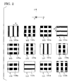
- Fig. 2 illustrates schematic xy sectional views of layers of the resonator shown in Fig. 1.
- Fig. 3 illustrates an enlarged view of a region around a point defect of the resonator shown in Fig. 1.
- Fig. 4 illustrates a graph showing a photonic band structure according to the first exemplary embodiment.
- Fig. 5 illustrates a graph showing the relationship between the defect mode frequencies and the length Dx, in the x-axis direction, of the point defect according to the first exemplary embodiment.
- Fig. 6 illustrates a graph showing the relationship between the defect mode frequencies and the length Dy, in the y-axis direction, of the point defect according to the first exemplary embodiment.
- Fig. 7 illustrates a graph showing the relationship between the defect mode frequencies and the thickness Dz of the point defect according to the first exemplary embodiment.
- Fig. 8 illustrates a spectrum of defect mode frequency according to the first exemplary embodiment.
- Fig. 9 illustrates a defect mode pattern of an xy section according to the first exemplary embodiment.
- Figs. 10A and 10B illustrate schematic representations of point defect arrangements.
- Fig. 11 illustrates a schematic representation of a resonator using a three-dimensional photonic crystal according to a second exemplary embodiment.
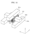
- Fig. 12 illustrates an enlarged view of a region around a point defect of the resonator shown in Fig. 11.
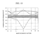
- Fig. 13 illustrates a graph showing a photonic band structure according to the second exemplary embodiment.
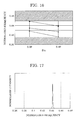
- Fig. 14 illustrates a graph showing the relationship between the defect mode frequencies and the length Dx, in the x-axis direction, of the point defect according to the second exemplary embodiment.
- Fig. 15 illustrates a graph showing the relationship between the defect mode frequencies and the length Dy, in the y-axis direction, of the point defect according to the second exemplary embodiment.
- Fig. 16 illustrates a graph showing the relationship between the defect mode frequencies and the thickness Dz of the point defect according to the second exemplary embodiment.
- Fig. 17 illustrates a spectrum of a defect mode according to the second exemplary embodiment.
- Fig. 18 illustrates a defect mode pattern of a xy section according to the second exemplary embodiment.
- Fig. 19 illustrates a schematic representation of a laser device.
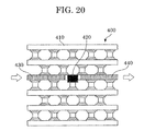
- Fig. 20 illustrates a schematic representation of a wavelength conversion device.
- columnar structures of a woodpile is one non-limiting example of a columnar structure, other non-limiting examples include non-columnar structures, nonuniform cross-sectional structures, other structures used in photonic crystals as known by one of ordinary skill in the relevant arts and equivalents.
- the actual size of structures may not be discussed however any size from micrometer (centimeter to meters) to nanometer and below sized photonic crystal structures are intended to lie within the scope of exemplary embodiments (e.g., photonic structures with characteristic sizes of individual molecules, nanometer size, micro size, centimeter, and meter sizes).
- exemplary embodiments are not limited to visual optical systems; photonic crystal structures can be constructed for use with infrared and other wavelength systems.
- an infrared light detector e.g., a detector measuring infrared markings.
- Fig. 1 illustrates a schematic representation of a resonator using a three-dimensional photonic crystal according to a first exemplary embodiment.
- the resonator 10 is produced by (i.e., includes) a point defect 120 formed in a periodic structure 100 or three-dimensional photonic crystal.
- the periodic structure 100 has a period comprising 12 layers in xy planes from a first layer 101 to a twelfth layer 112.
- Fig. 2 illustrates the xy sections of the 12 layers.
- the first layer 101 and the seventh layer 107 each contain a plurality of columnar structures 101a or 107a that are formed of a first medium (e.g., having a high refractive index) and extend in the y-axis direction and are arranged at regular intervals (lattice period) p in the x-axis direction.
- the columnar structures 101a of the first layer 101 are shifted by, for example, P/2 in the X-axis direction with respect to the columnar structures 107a of the seventh layer 107.
- the fourth layer 104 and the tenth layer 110 each contain a plurality of columnar structures 104a or 110a that are formed of a medium (e.g., the first medium) and extend in the x-axis direction and are arranged at regular intervals P in the y-axis direction.
- the columnar structures 104a of the forth layer 104 are shifted by, for example, P/2 in the y-axis direction with respect to the columnar structures 110a of the tenth layer 110.
- the second layer 102 and the third layer 103 which define an additional layer, each contain discrete structures 102a or 103a that are formed of the a medium (e.g., the first medium) and are separately disposed at positions in the xy planes, corresponding to the intersections of the columnar structures 101a of the first layer 101 and the columnar structures 104a of the fourth layer 104.
- the discrete structures 102a and the discrete structures 103a can be symmetrically disposed such as to be rotated at an angle of 90° with respect to each other in the respective xy planes.
- additional layers namely, the fifth layer 105 and sixth layer 106, the eighth layer 108 and ninth layer 109, and the eleventh layer 111 and twelfth layer 112, can each be disposed between the columnar structure-containing layers.
- additional layers e.g., 102, 103 are discussed between each pair of layers (e.g., 101 and 104), other exemplary embodiments can have one additional layer between one pair of layers, and not have subsequent additional layers, thus the discussion herein should not be interpreted to limit the number or arrangement of additional layers in exemplary embodiments.
- the layers (sublayers of the additional layers) 105, 106, 108, 109, 111, and 112 respectively can contain discrete structures 105a, 106a, 108a, 109a, 111a, and 112a that are formed of the a medium (e.g., the first medium) and are separately disposed in positions in the respective xy planes corresponding to the intersections of their adjacent columnar structure-containing layers, in the same manner.
- a medium e.g., the first medium
- An exemplary embodiment can have discrete structures made of a medium different than that from which any of the columnar structures are composed.
- the columnar structures in each layer can be in contact with the discrete structures in the adjacent additional layers.
- the regions other than the columnar structures or discrete plates in each layer are filled with a second medium (e.g., having a low refractive index).
- Parameters, such as the refractive indices of the first and second media, the shapes and intervals of the columnar structures and discrete structures, and the thicknesses of the layers, are optimally set so as to produce a wide complete photonic band gap in a desired frequency region (wavelength region).
- each layer can have columnar structures made of different materials, some can be made of the same, or even columnar structures within a layer can be made of different materials.
- a medium e.g., the first medium
- the second medium has a refractive index of about 1.
- the intervals between the columnar structures are P; each columnar structure-containing layer has a thickness, or length in the z direction, of 0.25 ⁇ P; each discrete-structure-containing layer has a thickness of 0.05 ⁇ P.
- Each columnar structure has a long rectangular solid shape with a height, or length in the z direction, of 0.25 ⁇ P and a width, or length in the x- or y-axis direction, of 0.3 ⁇ P.
- Each discrete structure has a rectangular solid shape with a thickness, or length in the z direction, of 0.05 ⁇ P and an xy cross section of 0.4 ⁇ P by 0.6 ⁇ P.
- Fig. 4 illustrates a photonic band structure of the periodic structure 100 calculated by a mathematical method (e.g., plane wave expansion method).
- the horizontal axis represents the wave number vector, that is, the direction in which electromagnetic waves propagate in the photonic crystal.
- K on the horizontal axis represents a wave number vector parallel to the x-axis direction (or y-axis direction)
- X on the horizontal axis represents a wave number vector in xy planes, forming an angle of 45° with the x axis (or y axis).
- the vertical axis represents the frequency normalized with the lattice period of the periodic structure.
- Fig. 4 shows that light entering from any direction cannot be present in the region indicated by hatching in the normalized frequency range of 0.34 to 0.42; hence, a complete photonic band gap is produced in this frequency range.
- a complete photonic band gap is produced in the wavelength region of 1.19 to 1.47 ⁇ m; when the intervals P are 200 nm, a complete photonic band gap is produced in the wavelength region of 480 to 590 nm.
- Fig. 3 illustrates an enlarged view of a region around the point defect 120.
- the point defect 120 is formed of a medium (e.g., the first medium) in a solid shape (e.g., rectangular) with a thickness Dz, a length Dx in the x-axis direction, and a length Dy in the y-axis direction.
- the point defect 120 facilitates the presence only therein of electromagnetic waves in a part of the wavelength region of the photonic band gap of the periodic structure 100.
- electromagnetic waves can be confined in a very small region, and the point defect 120 can serve as a high-performance resonator exhibiting a high confinement effect.
- defect mode The state in which electromagnetic waves are facilitated to be present in a photonic band gap that is caused by providing the point defect is hereinafter referred to as a defect mode; the frequency of the electromagnetic waves in this state is referred to as a defect mode frequency; and the distribution of electromagnetic energy in a resonator produced by the point defect is referred to as a defect mode pattern.
- Figs. 5 to 7 illustrate how the defect mode frequencies of the resonator 10 shown in Fig. 1 are changed depending on parameters of the shape of the point defect 120, according to the results of calculations by a mathematical method (e.g., the FDTD (Finite Difference Time Domain) method).
- FDTD Finite Difference Time Domain
- the point defect 120 used for the calculations is formed in two layers containing the columnar structures 104a and the discrete structures 103a such that the center coordinates in the x- and y-axis directions of the point defect 120 are the same as the center coordinates in the x- and y-axis directions of one of the discrete structures 103a.
- the hatched frequency regions in Fig. 5 represent frequencies outside the complete photonic band gap.
- the point defect 120 used for the calculations is formed in two layers containing the columnar structures 104a and the discrete structures 103a such that the center coordinates of the point defect 120 in the x- and y-axis directions are the same as the center coordinates in the x- and y-axis directions of one of the discrete structures 103a.
- the point defect 120 used for the calculations is formed such that its center coordinates in the x- and y-axis directions are the same as the center coordinates in the x- and y-axis directions of one of the discrete structures 103a, and such that its minimum coordinate in the z direction is the same as the minimum coordinate in the z direction of the columnar structures 104a.
- the variation in defect mode frequency for the shape of the point defect depends on the dimensional parameters. This suggests that the defect mode frequency can be controlled by varying the shape of the point defect.
- the manner of the changes in defect mode frequency for Dz values is distinguished from the manners of the changes for Dx and Dy values, as shown in Figs. 5 to 7. This distinction facilitates setting the defect mode frequencies with large intervals so that a designed defect mode frequency can be set with reduced influence of the adjacent defect modes.
- the point defect 120 can be formed in a discrete-structure-containing layer and its adjacent columnar structure-containing layer.
- the thickness Dz of the point defect 120 can be related to the sum of the thicknesses of the discrete-structure-containing layer and the columnar structure-containing layer.
- control of the defect mode frequency can be facilitated.
- Fig. 8 illustrates the spectrum of defect mode frequency of a periodic structure 100 formed at 8 periods in the x- and y-axis directions and 4 periods in the z direction with the point defect 120 at the center of the periodic structure
- Fig. 9 illustrates a defect mode pattern of an xy section of the periodic structure.
- the white region indicates a higher energy area and the black region indicates a lower energy area.
- Figs. 8 and 9 show that a highly symmetrical single defect mode can be achieved.
- the Q factor which represents a property of the light confinement of a resonator and is defined as the quotient of energy stored in a resonator divided by energy lost in a unit time from the resonator, of the defect mode shown in Fig. 8 is about 3,800.
- the Q factor is logarithmically increased by increasing the number of the period of the periodic structure 100.
- the Q factor can be increased to about 3 ⁇ 10 8 by setting the number of periods in the x- and y-axis directions at 20P and in the z direction at 16P.
- the number of periods of the periodic structure can be selected from numbers capable of producing a desired confinement effect.
- Designed defect mode frequencies can be obtained by designing the periodic structure under controlled conditions for example by controlling, the refractive indices of the first and second media, the shapes and intervals of the columnar structures and the discrete structures, and the thicknesses of the layers, so that a complete photonic band gap is produced in a frequency region including the designed defect mode frequency.
- controlled conditions can be used to form the point defect in at least one discrete-structure-containing layer at a thickness Dz different from the thickness of the columnar structure-containing layer.
- the designed defect mode frequencies can be achieved at desired intervals, with the symmetry of the defect mode pattern maintained.
- the resulting resonator can be of improved performance and exhibit an improved light confinement effect.
- the center of the point defect when the center of the point defect is positioned on an axis extending in the stacking direction from the center of an intersection of projections of the columnar structures, or on an axis extending in the stacking direction from a position shifted by chosen amount (e.g., P/2) from the center of an intersection of projections of the columnar structures in either of the directions in which the columnar structures are parallely arranged.
- the structural symmetry of the region around the point defect can be enhanced and, accordingly, the symmetry of the defect mode pattern increases, in comparison with the conventional system described in the background.
- the defect mode frequencies can be varied by changing the shape of the defect, facilitating the design of an increased performance resonator with the designed resonator frequency.
- the center of the point defect is positioned on an axis extending in the stacking direction of the layers from the center of an intersection of projections of the columnar structures, or on an axis extending in the stacking direction from a position shifted by a chosen amount (e.g., P/2) from the center of an intersection of projections of the columnar structures in either of the directions in which the columnar structures are parallely arranged.
- the position of the point defect may have an error of, for example, about ⁇ 0.1 ⁇ P with respect to the axis extending in the stacking direction.
- Exemplary embodiments include errors in the positioning of the point defect.
- the point defect can be formed in a discrete-structure-containing layer and its adjacent columnar structure-containing layer.
- the point defect may be formed in at least one discrete-structure-containing layer, as illustrated in Figs. 10A and 10B, depending on a designed frequency.
- the adjacent discrete-structure-containing layers for example, the second layer 102 and the third layer 103, define an additional layer, and the layers from the first layer 101 to the twelfth layer 112 define a unit of the periodic structure 100 (Fig. 1).
- the unit of the point defect structure may be defined by at least three layers including an additional layer and two columnar structure-containing layers.
- the additional layer includes at least one discrete-structure-containing layers.
- a three-dimensional photonic crystal including a first layer, a second layer, and an additional layer may be used for a functional device producing a relatively wide complete photonic band gap.
- the first layer includes a plurality of columnar structures arranged parallel to a first axis at a first predetermined interval.
- the second layer includes a plurality of columnar structures arranged parallel to a second axis at second predetermined intervals. Where in at least one exemplary embodiment the first and second predetermined intervals can be substantially equal. Similarly the third predetermined interval and the fourth predetermined interval can have the same or different value.
- the additional layer includes at least one sublayer containing discrete structures that can be separately arranged in a plane defined by the first and second axes. The first layer and the second layer are separated by the additional layer. The discrete structures can be disposed at positions corresponding to the intersections of projections of the columnar structures.
- the width of the photonic band gap can be increased.
- the reflectance of three-dimensional photonic crystal at a defect mode frequency can be increased, and its directional dependency can be reduced.
- a resonator in accordance with at least one exemplary embodiment can produce a resonator with an increased light confinement effect and/or exhibit high performance with a high Q factor.
- the defect mode frequencies can be controlled in a wide range.
- the manufacturing precision is increased by designing the thickness of the point defect to be substantially equal to the thickness of the additional layer or the sum of the thicknesses of a columnar structure-containing layer and its adjacent discrete-structure-containing layer.
- the shift of the columnar structures of the first layer 101 from the columnar structures of the seventh layer 107 and the shift of the columnar structures of the fourth layer 104 from the columnar structures of the tenth layer 110 can be by a chosen amount (e.g., substantially 1/2 of the interval P between the columnar structures).
- the periodic structure can be formed from at least two media with a high refractive index ratio.
- Exemplary high refractive index media include compound semiconductors such as GaAs, InP, and GaN, Si and other semiconductors, TiO 2 and similar dielectrics, metals, and other similar materials as known by one of ordinary skill in the relevant art and equivalents.
- Exemplary low refractive index media include SiO 2 and similar dielectrics, polymers such as polymethylmethacrylate (PMMA), gases (e.g., air), other similar materials as known by one of ordinary skill in the relevant art and equivalents.
- PMMA polymethylmethacrylate
- gases e.g., air
- the refractive index ratio can be at least 2.
- a high refractive index medium can be used as the first medium
- a low refractive index medium can be used as the second medium.
- medium 1 and medium 2 are not limited to this example, in accordance with the exemplary embodiment, can have a variety of refractive index values.
- the point defect can be formed of the same medium as the columnar structures and the discrete structure, the point defect may be formed of a medium having a different refractive index as well.
- Fig. 11 is a schematic illustration of a resonator according to a second exemplary embodiment.
- the resonator 20 can include a point defect 210 provided in a periodic structure 200.
- the periodic structure 200 can have a period defined by four (4) layers (each substantially parallel to the xy plane) from a first layer 201 to a fourth 204.
- the first layer 201 and the third layer 203 each can contain a plurality of columnar structures 201a or 203a (Fig. 12) that can be formed of a first medium (e.g., having a high refractive index) so as to extend in the x-axis direction and can be arranged at regular intervals (lattice period) P in the y-axis direction.
- a first medium e.g., having a high refractive index
- the columnar structures 201a of the first layer 201 can be shifted, (e.g., P/2 in the y-axis direction) with respect to the columnar structures 203a of the third layer 203.
- the second layer 202 and the fourth layer 204 each contain a plurality of columnar structures (e.g., 202a) that can be formed of the first medium so as to extend in the y-axis direction and are arranged at regular intervals P in the x-axis direction.
- the columnar structures 202a of the second layer 202 are shifted (e.g., P/2 in the x-axis direction) with respect to the columnar structures 204a of the fourth layer 204.
- the regions other than the columnar structures in each layer can be filled with a second medium (e.g., having a low refractive index).
- Conditions such as the refractive indices of the first and second media, the shape and intervals of the columnar structures, and the thicknesses of the layers, can be set so as to produce a wide complete photonic band gap in a designed frequency region (wavelength region).
- the refractive index of the first medium is set at about 3.3
- the refractive index of the second medium is set at about 1.
- the intervals between the columnar structures are P.
- Each columnar structure has a long rectangular solid shape with a height, or length in the z direction, of 0.3 ⁇ P and a width, or length in the x- or y-axis direction, of 0.25 ⁇ P.
- Fig. 13 illustrates the photonic band structure of the periodic structure 200 calculated by a mathematical method (e.g., plane wave expansion method).
- the horizontal axis represents the wave number vector, that is, the direction in which electromagnetic waves propagate in the photonic crystal.
- K on the horizontal axis represents a wave number vector parallel to the x-axis direction (or y-axis direction)
- X on the horizontal axis represents a wave number vector in xy planes, forming an angle of 45° with the x axis (or y axis).
- the vertical axis represents the frequency normalized with the lattice period of the periodic structure.
- Fig. 13 shows that light entering from any direction cannot be present in the region indicated by hatching in the normalized frequency range of 0.39 to 0.46; hence, a complete photonic band gap is produced in this frequency range.
- a complete photonic band gap is produced in the wavelength region of 1.09 to 1.28 ⁇ m; when the intervals P are 250 nm, a complete photonic band gap is produced in the wavelength region of 540 to 640 nm.
- Fig. 12 is an enlarged view of a region around the point defect 210.
- the point defect 210 can be formed of the same medium as the columnar structures, in the example illustrated the point defect is a rectangular solid shape with a thickness Dz1, a length Dx1 in the x-axis direction, and a length Dy1 in the y-axis direction, so as to partially contain one of the columnar structures.
- the point defect 210 facilitates the presence of electromagnetic waves in a part of the wavelength region of the photonic band gap of the periodic structure 200.
- electromagnetic waves can be confined in a very small region, and the point defect 210 can serve as a resonator exhibiting an improved confinement effect.
- Figs. 14 to 16 show how the defect mode frequencies of the resonator 20 shown illustrated Fig. 11 are changed depending on parameters of the shape of the point defect 210, according to the results of calculations by a mathematical method (e.g., the FDTD method).
- a mathematical method e.g., the FDTD method
- the point defect 210 used for the measurements is formed in the layer containing the columnar structures 202a such that the center coordinate in the x-axis direction of the point defect 210 is the same as the center coordinates in the x-axis direction of one of the columnar structures 202a, and such that the center coordinate in the y-axis direction of the point defect 210 is substantially the same as the center coordinate in the y-axis direction of one of the columnar structures 201a.
- the hatched frequency regions in Fig. 14 are outside the complete photonic band gap.
- the point defect 210 used for the calculations is formed in the layer containing the columnar structures 202a such that the center coordinate in the x-axis direction of the point defect is substantially the same as the center coordinate in the x-axis direction of one of the columnar structures 202a, and such that the center coordinate of the defect in the y-axis direction is the same as the center coordinate in the y-axis direction of one of the columnar structures 201a.
- the point defect 210 used for the measurements is formed such its center coordinate in the x-axis direction is the same as the center coordinate in the x-axis direction of one of the columnar structures 202a, such that the center coordinate in the y-axis direction of the point defect 210 is substantially the same as the center coordinate in the y-axis direction of one of the columnar structures 201a, and such that the maximum coordinate in the z direction of the point defect 210 is the same as the maximum coordinate in the z direction of the columnar structure 202a.
- the complete photonic band gap of the second exemplary embodiment can produce a frequency region including a desired defect mode frequency, by controlling conditions of the second exemplary embodiment, such as the refractive indices of the first and second media of the periodic structure, the shape of and interval between the columnar structures, and the thickness of the layers.
- the defect mode frequencies can be controlled in a wider range, and designed defect mode frequencies can be achieved at designed intervals, with the symmetry of the defect mode pattern maintained.
- the columnar structures and the point defect are not necessarily formed of the same medium, as in the first exemplary embodiment.
- the above dimensions for the point defect 210 are intended for illustration only and not as limiting factors.
- FIG. 17 illustrates the spectrum of defect mode frequency of a periodic structure 200 formed at 8 periods in the x- and y-axis directions and 4 periods of the z direction with the point defect 210 at the center of the periodic structure 200
- Fig. 18 illustrates a defect mode pattern of an xy section of the periodic structure. Figs. 17 and 18 show that a highly symmetrical single defect mode pattern has been achieved.
- the point defect of the three-dimensional photonic crystal according to the first or the second exemplary embodiment can be filled with an active medium capable of emitting light, and energy, such as electromagnetic waves or current, when driven by a driver.
- an increased efficient light emitting device e.g., a laser, an LED, other light emitting devices as known by one of ordinary skill in the relevant arts, and equivalents
- a laser e.g., a laser, an LED, other light emitting devices as known by one of ordinary skill in the relevant arts, and equivalents
- the active medium can be selected from, for example, materials having a multi-quantum well structure or multi-quantum dot structure, such as InGaAsP, AlGaAs, AlGaInP, AlGaN, InGaN, ZnSe, and ZnS, organic materials, other multi-quantum well or dot structures as known by one of ordinary skill in the relevant art and equivalents, according to the designed resonant wavelength.
- a multi-quantum well structure or multi-quantum dot structure such as InGaAsP, AlGaAs, AlGaInP, AlGaN, InGaN, ZnSe, and ZnS, organic materials, other multi-quantum well or dot structures as known by one of ordinary skill in the relevant art and equivalents, according to the designed resonant wavelength.
- Fig. 19 illustrates the structure of a laser device having an active portion that emits light by carrier injection, in a point defect.
- the laser device 300 includes a resonator prepared by forming a point defect 320 in a periodic structure 310 according to the first or the second exemplary embodiment, a p-type electrode 331, a p-type carrier conduction path 330, an n-type electrode 341, an n-type carrier conduction path 340, and a waveguide 350.
- the resonator has an active portion inside that emits light by carrier injection.
- the waveguide 350 can be produced by a linear defect that can be formed in the periodic structure 310 so as to disturb the periodicity.
- the wavelength of the waveguide mode can be set so as to increase the combination efficiency with the resonator, in consideration of the resonance mode, by varying the shape and refractive index of the linear defect.
- the linear defect can be formed by changing the shape or refractive index of some of the columnar structures in the periodic structure 310, or by providing an additional columnar structure.
- Holes can be supplied to the resonator through the p-type electrode 331 and the p-type carrier conduction path 330, and electrons can be supplied to the resonator through the n-type electrode 341 and the n-type carrier conduction path 340.
- the holes and electrons can be combined in the resonator to emit light or generate laser light, and the light can be extracted through the waveguide 350.
- the point defect in the three-dimensional photonic crystal according to the first or the second exemplary embodiment may be filled with a nonlinear material, and energy, such as the electromagnetic waves or current, may be supplied to the nonlinear material. Since this structure can confine light with a strong energy in a very narrow region, the resulting nonlinear optical device can produce increased nonlinear optical effects.
- the nonlinear material may be LiNbO 3 , LiTaO 3 , BaTiO 3 , ZnO, BaB 2 O 4 , BiB 3 O 6 , KTiOPO 4 , or other nonlinear material as known by one of ordinary skill in the relevant art or equivalents.
- Fig. 20 illustrates a wavelength conversion device 400 using the nonlinear optical effect.
- the wavelength conversion device 400 includes a resonator prepared by forming a point defect 420 in a periodic structure 410 according to the first or the second exemplary embodiment, an input waveguide 430, and an output waveguide 440.
- the inside of the resonator can be filled with a nonlinear material.
- the input waveguide 430 and the output waveguide 440 can each be produced by a linear defect that can be formed in the periodic structure 410 so as to disturb the periodicity.
- the wavelength of the waveguide mode can be selected according to, for example, the shape and refractive index of the linear defect.
- Light introduced into the input waveguide 430 from the outside e.g., through a lens or a fiber
- the harmonics are extracted through the output waveguide 440.
- the guided wavelength region of the input waveguide 430 can be set so as to include the wavelength of the incident light, not including the wavelength of the converted light
- the guided wavelength region of the output waveguide 440 can be set so as to include the wavelength of the converted light, not including the wavelength of the incident light.
- the wavelength of incident light can be efficiently converted and the converted light can efficiently be extracted.
- Light having a plurality of wavelengths may be used. This light can be converted by use of a nonlinear effect of light other than harmonics, such as sum of light frequencies or difference frequency light, and can then be extracted.
- the three-dimensional photonic crystal optical resonators 10 and 20 according to the first and the second exemplary embodiment can be used as part of wavelength selection filters.
- the wavelength selection filters can output light with a frequency with high selectivity, according to the defect mode.
- optical functional devices can be combined to prepare an optical circuit.
- the size of the optical circuit can be further reduced.
- Exemplary embodiments can use three-dimensional photonic crystals with point defects that can serve as a resonator having designed defect mode frequencies at designed intervals, while maintaining the symmetry of the defect mode patterns.
- the resonator can be of increased performance and exhibits an increased light confinement effect over some conventional systems.
- the laser can oscillate at a desired wavelength with high efficiency.
- the resonator according to the present invention can achieve highly functional optical devices.
- Exemplary embodiments are capable of being used in many devices, for example in light emitting devices and wavelength conversion devices.
- the phrase “layer are orthogonal” is intended to include arrangements where the "layer is substantially orthogonal” and the term “extending in the same direction” is intended to include the arrangements "extending in about the same direction.”
- the intended scope is meant to include the same direction and orthogonal within a variance of the true same direction or orthogonal position (e.g., a few degrees inclination).
- the term “one-half of” is intended to include arrangements of "about one-half” (i.e., one-half within a variance (e.g., 1% of 1 ⁇ 2)).
Landscapes
- Physics & Mathematics (AREA)
- Optics & Photonics (AREA)
- Engineering & Computer Science (AREA)
- General Physics & Mathematics (AREA)
- Chemical & Material Sciences (AREA)
- Nanotechnology (AREA)
- Biophysics (AREA)
- Crystallography & Structural Chemistry (AREA)
- Condensed Matter Physics & Semiconductors (AREA)
- Life Sciences & Earth Sciences (AREA)
- Electromagnetism (AREA)
- Microelectronics & Electronic Packaging (AREA)
- Semiconductor Lasers (AREA)
- Optical Integrated Circuits (AREA)
- Lasers (AREA)
Abstract
Description
- The present invention relates to a resonator using a three-dimensional photonic crystal, more particularly, though not exclusively, the present invention relates to a resonator formed from a defect in a photonic crystal.
- Yablonovitch has proposed an idea of controlling the transmission and reflection characteristics of electromagnetic waves by structures smaller than or equal to a wavelength in Physical Review Letters, Vol. 58, p. 2059, 1987. This document has taught that the transmission and reflection characteristics of electromagnetic waves can be controlled by periodically arranging structures smaller than or equal to a wavelength. A photonic crystal can be such a unit of periodically arranged structures, and suggests that a reflection mirror exhibiting no optical loss, namely, a reflectance of about 100%, can be achieved in a specific wavelength region. This region is referred to as a photonic band gap, likened to an energy gap of a semiconductor. In particular, a three-dimensional microscopic periodic structure can produce a photonic band gap for all the light entering from any direction (hereinafter referred to as complete photonic band gap). The complete photonic band gap can have various applications (e.g., light emitting devices, control of spontaneous emission).
- Woodpile structures in which columnar structures are periodically stacked in a layered manner have been discussed in, for example, U.S. patent No. 5,335,240 and Japanese Patent Laid-Open No. 2004-6567. Japanese Patent Laid-Open No. 2004-6567 has also discussed a resonator using a woodpile structure having a defect inside. The defect is formed in a rectangular solid shape with the same thickness as that of the columnar structure, and is present among the columnar structures. In general, a resonator produced by a defect formed in a photonic crystal has plural resonance modes. Resonators used in light emitting devices or wavelength selection filters have designed confinement effects and satisfy resonance requirements for a designed resonant wavelength. In addition, in order to avoid the influence of other resonance modes having a wavelength close to the designed wavelength, for example, to reduce the effect of mode hopping in a laser, one can provide a large difference between the designed resonant wavelength and the wavelengths of the resonant in the other resonance modes.
- The periodicity around the defect of the periodic structure can be increased to increase the reflectance. Japanese Patent Laid-Open No. 2004-6567 has also discussed another approach in which the difference in resonant wavelength between adjacent resonance modes is controlled by varying the lengths of two sides other than the thickness of rectangular solid defect, and by shifting the position of the defect with respect to the columnar structures. Unfortunately, the shift of the position of the defect makes the periodic structure asymmetrical, so that the energy distribution of the electromagnetic field in the resonator is also made asymmetrical. If the resonator is used in a laser, such asymmetry causes a large deflection of the orientation of the emitted light and may result in a critical problem. In addition, the maximum of the shift in the position of the defect is 1/4 of the period of columnar structure arrangement, making the choices of designed resonant wavelength limited.
- Accordingly, an exemplary embodiment is directed to a resonator resonating in a single mode with a symmetrical energy distribution of an electromagnetic field.
- At least one exemplary embodiment is directed to a resonator, which can be by a point defect formed in a three-dimensional photonic crystal. The three-dimensional photonic crystal can include a first layer to a fourth layer. The first layer includes a plurality of columnar structures spaced apart by a first predetermined interval. The second layer includes a plurality of columnar structures spaced apart by a second predetermined interval, the columnar structures of the second layer extending in a direction different from that of the columnar structures in the first layer. The third layer includes a plurality of columnar structures spaced apart by a third predetermined interval, the columnar structures of the third layer extending in about the same direction as that of the columnar structures in the first layer. The fourth layer includes a plurality of columnar structures spaced apart by a fourth predetermined interval, the columnar structures extending in substantially the same direction as that of the columnar structures in the second layer. The first to fourth layers can be stacked such that the columnar structures of the first layer are shifted by about half of the regular interval in the direction substantially perpendicular to the direction of the extension of the columnar structures of the first and third layers, and such that the columnar structures of the second layer are shifted by about half of the regular interval in the direction perpendicular to the direction of the extension of the columnar structures of the fourth layer. The point defect can have a thickness different from each thickness of the four layers.
- Further features of the present invention will become apparent from the following description of exemplary embodiments with reference to the attached drawings.
- Fig. 1 illustrates a schematic illustration of a resonator using a three-dimensional photonic crystal according to a first exemplary embodiment.
- Fig. 2 illustrates schematic xy sectional views of layers of the resonator shown in Fig. 1.
- Fig. 3 illustrates an enlarged view of a region around a point defect of the resonator shown in Fig. 1.
- Fig. 4 illustrates a graph showing a photonic band structure according to the first exemplary embodiment.
- Fig. 5 illustrates a graph showing the relationship between the defect mode frequencies and the length Dx, in the x-axis direction, of the point defect according to the first exemplary embodiment.
- Fig. 6 illustrates a graph showing the relationship between the defect mode frequencies and the length Dy, in the y-axis direction, of the point defect according to the first exemplary embodiment.
- Fig. 7 illustrates a graph showing the relationship between the defect mode frequencies and the thickness Dz of the point defect according to the first exemplary embodiment.
- Fig. 8 illustrates a spectrum of defect mode frequency according to the first exemplary embodiment.
- Fig. 9 illustrates a defect mode pattern of an xy section according to the first exemplary embodiment.
- Figs. 10A and 10B illustrate schematic representations of point defect arrangements.
- Fig. 11 illustrates a schematic representation of a resonator using a three-dimensional photonic crystal according to a second exemplary embodiment.
- Fig. 12 illustrates an enlarged view of a region around a point defect of the resonator shown in Fig. 11.
- Fig. 13 illustrates a graph showing a photonic band structure according to the second exemplary embodiment.
- Fig. 14 illustrates a graph showing the relationship between the defect mode frequencies and the length Dx, in the x-axis direction, of the point defect according to the second exemplary embodiment.
- Fig. 15 illustrates a graph showing the relationship between the defect mode frequencies and the length Dy, in the y-axis direction, of the point defect according to the second exemplary embodiment.
- Fig. 16 illustrates a graph showing the relationship between the defect mode frequencies and the thickness Dz of the point defect according to the second exemplary embodiment.
- Fig. 17 illustrates a spectrum of a defect mode according to the second exemplary embodiment.
- Fig. 18 illustrates a defect mode pattern of a xy section according to the second exemplary embodiment.
- Fig. 19 illustrates a schematic representation of a laser device.
- Fig. 20 illustrates a schematic representation of a wavelength conversion device.
- The following description of at least one of the possible exemplary embodiment(s) is merely illustrative in nature and is in no way intended to limit the invention, its application, its equivalents, or uses.
- Processes, techniques, apparatus, and materials as known by one of ordinary skill in the art may not be discussed in detail but are intended to be part of the enabling description where appropriate. For example some examples of photonic crystal formation are discussed, equivalents and other photonic crystal configurations and materials used, as known by one of ordinary skill in the relevant arts, are intended to be included in the scope of at least a few exemplary embodiments.
- Additionally, referral is made herein of columnar structures. The columnar structures of a woodpile is one non-limiting example of a columnar structure, other non-limiting examples include non-columnar structures, nonuniform cross-sectional structures, other structures used in photonic crystals as known by one of ordinary skill in the relevant arts and equivalents.
- Additionally, the actual size of structures may not be discussed however any size from micrometer (centimeter to meters) to nanometer and below sized photonic crystal structures are intended to lie within the scope of exemplary embodiments (e.g., photonic structures with characteristic sizes of individual molecules, nanometer size, micro size, centimeter, and meter sizes).
- Additionally, exemplary embodiments are not limited to visual optical systems; photonic crystal structures can be constructed for use with infrared and other wavelength systems. For example an infrared light detector (e.g., a detector measuring infrared markings).
- Fig. 1 illustrates a schematic representation of a resonator using a three-dimensional photonic crystal according to a first exemplary embodiment. The
resonator 10 is produced by (i.e., includes) apoint defect 120 formed in aperiodic structure 100 or three-dimensional photonic crystal. Theperiodic structure 100 has a period comprising 12 layers in xy planes from afirst layer 101 to atwelfth layer 112. Fig. 2 illustrates the xy sections of the 12 layers. Thefirst layer 101 and theseventh layer 107 each contain a plurality ofcolumnar structures columnar structures 101a of thefirst layer 101 are shifted by, for example, P/2 in the X-axis direction with respect to thecolumnar structures 107a of theseventh layer 107. Thefourth layer 104 and thetenth layer 110 each contain a plurality ofcolumnar structures columnar structures 104a of theforth layer 104 are shifted by, for example, P/2 in the y-axis direction with respect to thecolumnar structures 110a of thetenth layer 110. Thesecond layer 102 and thethird layer 103, which define an additional layer, each containdiscrete structures columnar structures 101a of thefirst layer 101 and thecolumnar structures 104a of thefourth layer 104. Thediscrete structures 102a and thediscrete structures 103a can be symmetrically disposed such as to be rotated at an angle of 90° with respect to each other in the respective xy planes. Other additional layers, namely, thefifth layer 105 andsixth layer 106, theeighth layer 108 andninth layer 109, and theeleventh layer 111 andtwelfth layer 112, can each be disposed between the columnar structure-containing layers. Note that although additional layers (e.g., 102, 103) are discussed between each pair of layers (e.g., 101 and 104), other exemplary embodiments can have one additional layer between one pair of layers, and not have subsequent additional layers, thus the discussion herein should not be interpreted to limit the number or arrangement of additional layers in exemplary embodiments. - The layers (sublayers of the additional layers) 105, 106, 108, 109, 111, and 112 respectively can contain
discrete structures - Note that some layers have columnar structures, in the example of
exemplary embodiment 1 discussed, made of the same medium. This is for illustrative purposes only and the columnar structures can be made of different materials. For example, each layer can have columnar structures made of different materials, some can be made of the same, or even columnar structures within a layer can be made of different materials. - Also note that a shift of P/2 is discussed, however various shift values can be used depending upon the design, and the discussion herein should not be interpreted to limit the amount of shifts between layers.
- In the example of a first exemplary embodiment, a medium (e.g., the first medium) has a refractive index of about 3.3, and the second medium has a refractive index of about 1. The intervals between the columnar structures are P; each columnar structure-containing layer has a thickness, or length in the z direction, of 0.25×P; each discrete-structure-containing layer has a thickness of 0.05×P. Each columnar structure has a long rectangular solid shape with a height, or length in the z direction, of 0.25×P and a width, or length in the x- or y-axis direction, of 0.3×P. Each discrete structure has a rectangular solid shape with a thickness, or length in the z direction, of 0.05×P and an xy cross section of 0.4×P by 0.6×P. Fig. 4 illustrates a photonic band structure of the
periodic structure 100 calculated by a mathematical method (e.g., plane wave expansion method). In Fig. 4, the horizontal axis represents the wave number vector, that is, the direction in which electromagnetic waves propagate in the photonic crystal. For example, K on the horizontal axis represents a wave number vector parallel to the x-axis direction (or y-axis direction), and X on the horizontal axis represents a wave number vector in xy planes, forming an angle of 45° with the x axis (or y axis). The vertical axis represents the frequency normalized with the lattice period of the periodic structure. Fig. 4 shows that light entering from any direction cannot be present in the region indicated by hatching in the normalized frequency range of 0.34 to 0.42; hence, a complete photonic band gap is produced in this frequency range. For example, when the intervals P between the columnar structures are 0.5 µm, a complete photonic band gap is produced in the wavelength region of 1.19 to 1.47 µm; when the intervals P are 200 nm, a complete photonic band gap is produced in the wavelength region of 480 to 590 nm. - Note that the rectangular discrete structures illustrated in the example of the first exemplary embodiment are for illustrative, non-limiting, purposes only. In actuality the shape of the discrete structures are not limited in exemplary embodiments.
- Fig. 3 illustrates an enlarged view of a region around the
point defect 120. Thepoint defect 120 is formed of a medium (e.g., the first medium) in a solid shape (e.g., rectangular) with a thickness Dz, a length Dx in the x-axis direction, and a length Dy in the y-axis direction. Thepoint defect 120 facilitates the presence only therein of electromagnetic waves in a part of the wavelength region of the photonic band gap of theperiodic structure 100. Thus, electromagnetic waves can be confined in a very small region, and thepoint defect 120 can serve as a high-performance resonator exhibiting a high confinement effect. The state in which electromagnetic waves are facilitated to be present in a photonic band gap that is caused by providing the point defect is hereinafter referred to as a defect mode; the frequency of the electromagnetic waves in this state is referred to as a defect mode frequency; and the distribution of electromagnetic energy in a resonator produced by the point defect is referred to as a defect mode pattern. - Figs. 5 to 7 illustrate how the defect mode frequencies of the
resonator 10 shown in Fig. 1 are changed depending on parameters of the shape of thepoint defect 120, according to the results of calculations by a mathematical method (e.g., the FDTD (Finite Difference Time Domain) method). Fig. 5 illustrates the relationship between the defect mode frequencies and length Dx when the dimensions of the point defect are Dz = 0.3xP and Dx = Dy. For example, referring to Fig. 3, thepoint defect 120 used for the calculations is formed in two layers containing thecolumnar structures 104a and thediscrete structures 103a such that the center coordinates in the x- and y-axis directions of thepoint defect 120 are the same as the center coordinates in the x- and y-axis directions of one of thediscrete structures 103a. The hatched frequency regions in Fig. 5 represent frequencies outside the complete photonic band gap. Fig. 6 illustrates the relationship between the defect mode frequencies and length Dy when the dimensions of the point defect are Dz = 0.3×P and Dx = 0.8×P. For example, referring to Fig. 3, thepoint defect 120 used for the calculations is formed in two layers containing thecolumnar structures 104a and thediscrete structures 103a such that the center coordinates of thepoint defect 120 in the x- and y-axis directions are the same as the center coordinates in the x- and y-axis directions of one of thediscrete structures 103a. Fig. 7 illustrates the relationship between the defect mode frequencies and length Dz when the dimensions of the point defect are Dx = 0.8×P and Dy = 0.8×P. For example, referring to Fig. 3, thepoint defect 120 used for the calculations is formed such that its center coordinates in the x- and y-axis directions are the same as the center coordinates in the x- and y-axis directions of one of thediscrete structures 103a, and such that its minimum coordinate in the z direction is the same as the minimum coordinate in the z direction of thecolumnar structures 104a. The variation in defect mode frequency for the shape of the point defect depends on the dimensional parameters. This suggests that the defect mode frequency can be controlled by varying the shape of the point defect. The manner of the changes in defect mode frequency for Dz values is distinguished from the manners of the changes for Dx and Dy values, as shown in Figs. 5 to 7. This distinction facilitates setting the defect mode frequencies with large intervals so that a designed defect mode frequency can be set with reduced influence of the adjacent defect modes. - For example, a single defect mode can be produced in the photonic band gap, that is, a single mode can be achieved, by designing the
point defect 120 in Fig. 3 at dimensions of Dx = P, Dy = 0.3×P, and Dz = 0.35×P such that its center coordinates in the x- and y-axis directions are the same as the center coordinates in the x- and y-axis directions of one of thediscrete structures 103a, and such that its minimum coordinate in the z direction is the same as the minimum coordinate in the z direction of thecolumnar structures 104a. In this instance, thepoint defect 120 can be formed in a discrete-structure-containing layer and its adjacent columnar structure-containing layer. In view of the manufacturing process, the thickness Dz of thepoint defect 120 can be related to the sum of the thicknesses of the discrete-structure-containing layer and the columnar structure-containing layer. By forming the point defect in a columnar structure-containing layer and at least one discrete-structure-containing layer (e.g., where the discrete-structure-containing layer has a thickness smaller than that of the columnar structure-containing layer), control of the defect mode frequency can be facilitated. Fig. 8 illustrates the spectrum of defect mode frequency of aperiodic structure 100 formed at 8 periods in the x- and y-axis directions and 4 periods in the z direction with thepoint defect 120 at the center of the periodic structure, while Fig. 9 illustrates a defect mode pattern of an xy section of the periodic structure. In Fig. 9, the white region indicates a higher energy area and the black region indicates a lower energy area. Figs. 8 and 9 show that a highly symmetrical single defect mode can be achieved. - The Q factor, which represents a property of the light confinement of a resonator and is defined as the quotient of energy stored in a resonator divided by energy lost in a unit time from the resonator, of the defect mode shown in Fig. 8 is about 3,800. The Q factor is logarithmically increased by increasing the number of the period of the
periodic structure 100. For example, the Q factor can be increased to about 3×10⁸ by setting the number of periods in the x- and y-axis directions at 20P and in the z direction at 16P. The number of periods of the periodic structure can be selected from numbers capable of producing a desired confinement effect. - Designed defect mode frequencies can be obtained by designing the periodic structure under controlled conditions for example by controlling, the refractive indices of the first and second media, the shapes and intervals of the columnar structures and the discrete structures, and the thicknesses of the layers, so that a complete photonic band gap is produced in a frequency region including the designed defect mode frequency. Where controlled conditions can be used to form the point defect in at least one discrete-structure-containing layer at a thickness Dz different from the thickness of the columnar structure-containing layer. In at least one exemplary embodiment, the designed defect mode frequencies can be achieved at desired intervals, with the symmetry of the defect mode pattern maintained. Thus, the resulting resonator can be of improved performance and exhibit an improved light confinement effect. In particular, when the center of the point defect is positioned on an axis extending in the stacking direction from the center of an intersection of projections of the columnar structures, or on an axis extending in the stacking direction from a position shifted by chosen amount (e.g., P/2) from the center of an intersection of projections of the columnar structures in either of the directions in which the columnar structures are parallely arranged. The structural symmetry of the region around the point defect can be enhanced and, accordingly, the symmetry of the defect mode pattern increases, in comparison with the conventional system described in the background. In further exemplary embodiments, the defect mode frequencies can be varied by changing the shape of the defect, facilitating the design of an increased performance resonator with the designed resonator frequency.
- In the above description, the center of the point defect is positioned on an axis extending in the stacking direction of the layers from the center of an intersection of projections of the columnar structures, or on an axis extending in the stacking direction from a position shifted by a chosen amount (e.g., P/2) from the center of an intersection of projections of the columnar structures in either of the directions in which the columnar structures are parallely arranged. In practice, however, the position of the point defect may have an error of, for example, about ±0.1×P with respect to the axis extending in the stacking direction. Exemplary embodiments include errors in the positioning of the point defect.
- In at least one exemplary embodiment, the point defect can be formed in a discrete-structure-containing layer and its adjacent columnar structure-containing layer. To facilitate control the defect mode frequencies by varying the thickness of the point defect, the point defect may be formed in at least one discrete-structure-containing layer, as illustrated in Figs. 10A and 10B, depending on a designed frequency.
- In at least one exemplary embodiment, the adjacent discrete-structure-containing layers, for example, the
second layer 102 and thethird layer 103, define an additional layer, and the layers from thefirst layer 101 to thetwelfth layer 112 define a unit of the periodic structure 100 (Fig. 1). Alternatively, the unit of the point defect structure may be defined by at least three layers including an additional layer and two columnar structure-containing layers. In this instance, the additional layer includes at least one discrete-structure-containing layers. For example, a three-dimensional photonic crystal including a first layer, a second layer, and an additional layer may be used for a functional device producing a relatively wide complete photonic band gap. The first layer includes a plurality of columnar structures arranged parallel to a first axis at a first predetermined interval. The second layer includes a plurality of columnar structures arranged parallel to a second axis at second predetermined intervals. Where in at least one exemplary embodiment the first and second predetermined intervals can be substantially equal. Similarly the third predetermined interval and the fourth predetermined interval can have the same or different value. The additional layer includes at least one sublayer containing discrete structures that can be separately arranged in a plane defined by the first and second axes. The first layer and the second layer are separated by the additional layer. The discrete structures can be disposed at positions corresponding to the intersections of projections of the columnar structures. By increasing the number of discrete-structure-containing sublayers in the additional layer, the width of the photonic band gap can be increased. By use of an additional layer including at least two discrete-structure-containing sublayers, the reflectance of three-dimensional photonic crystal at a defect mode frequency can be increased, and its directional dependency can be reduced. Thus, a resonator in accordance with at least one exemplary embodiment can produce a resonator with an increased light confinement effect and/or exhibit high performance with a high Q factor. Also, since the three-dimensional photonic crystal can have a wide photonic band gap, the defect mode frequencies can be controlled in a wide range. For example, in at least one exemplary embodiment, the manufacturing precision is increased by designing the thickness of the point defect to be substantially equal to the thickness of the additional layer or the sum of the thicknesses of a columnar structure-containing layer and its adjacent discrete-structure-containing layer. - In exemplary embodiments, the shift of the columnar structures of the
first layer 101 from the columnar structures of theseventh layer 107 and the shift of the columnar structures of thefourth layer 104 from the columnar structures of thetenth layer 110 can be by a chosen amount (e.g., substantially 1/2 of the interval P between the columnar structures). - The periodic structure can be formed from at least two media with a high refractive index ratio. Exemplary high refractive index media include compound semiconductors such as GaAs, InP, and GaN, Si and other semiconductors, TiO2 and similar dielectrics, metals, and other similar materials as known by one of ordinary skill in the relevant art and equivalents. Exemplary low refractive index media include SiO2 and similar dielectrics, polymers such as polymethylmethacrylate (PMMA), gases (e.g., air), other similar materials as known by one of ordinary skill in the relevant art and equivalents. The photonic band gap of a photonic crystal results from the distribution of dielectric constants in the crystal. Combined use of media having an increased dielectric constant ratio leads to a wider complete photonic band gap. In at least one exemplary embodiment, the refractive index ratio can be at least 2. In the above example of the first exemplary embodiment, a high refractive index medium can be used as the first medium, and a low refractive index medium can be used as the second medium. However,
medium 1 and medium 2 are not limited to this example, in accordance with the exemplary embodiment, can have a variety of refractive index values. - Although, in the above example of the first exemplary embodiment, the point defect can be formed of the same medium as the columnar structures and the discrete structure, the point defect may be formed of a medium having a different refractive index as well.
- Second Exemplary Embodiment
- Fig. 11 is a schematic illustration of a resonator according to a second exemplary embodiment. The
resonator 20 can include apoint defect 210 provided in aperiodic structure 200. Theperiodic structure 200 can have a period defined by four (4) layers (each substantially parallel to the xy plane) from afirst layer 201 to a fourth 204. Thefirst layer 201 and thethird layer 203 each can contain a plurality ofcolumnar structures columnar structures 201a of thefirst layer 201 can be shifted, (e.g., P/2 in the y-axis direction) with respect to thecolumnar structures 203a of thethird layer 203. Thesecond layer 202 and thefourth layer 204 each contain a plurality of columnar structures (e.g., 202a) that can be formed of the first medium so as to extend in the y-axis direction and are arranged at regular intervals P in the x-axis direction. Thecolumnar structures 202a of thesecond layer 202 are shifted (e.g., P/2 in the x-axis direction) with respect to the columnar structures 204a of thefourth layer 204. The regions other than the columnar structures in each layer can be filled with a second medium (e.g., having a low refractive index). Conditions, such as the refractive indices of the first and second media, the shape and intervals of the columnar structures, and the thicknesses of the layers, can be set so as to produce a wide complete photonic band gap in a designed frequency region (wavelength region). In the example of the second exemplary embodiment, the refractive index of the first medium is set at about 3.3, and the refractive index of the second medium is set at about 1. The intervals between the columnar structures are P. Each columnar structure has a long rectangular solid shape with a height, or length in the z direction, of 0.3×P and a width, or length in the x- or y-axis direction, of 0.25×P. Fig. 13 illustrates the photonic band structure of theperiodic structure 200 calculated by a mathematical method (e.g., plane wave expansion method). In Fig. 13, the horizontal axis represents the wave number vector, that is, the direction in which electromagnetic waves propagate in the photonic crystal. For example, K on the horizontal axis represents a wave number vector parallel to the x-axis direction (or y-axis direction), and X on the horizontal axis represents a wave number vector in xy planes, forming an angle of 45° with the x axis (or y axis). The vertical axis represents the frequency normalized with the lattice period of the periodic structure. Fig. 13 shows that light entering from any direction cannot be present in the region indicated by hatching in the normalized frequency range of 0.39 to 0.46; hence, a complete photonic band gap is produced in this frequency range. For example, when the intervals P between the columnar structures are 0.5 µm, a complete photonic band gap is produced in the wavelength region of 1.09 to 1.28 µm; when the intervals P are 250 nm, a complete photonic band gap is produced in the wavelength region of 540 to 640 nm. - Fig. 12 is an enlarged view of a region around the
point defect 210. Thepoint defect 210 can be formed of the same medium as the columnar structures, in the example illustrated the point defect is a rectangular solid shape with a thickness Dz1, a length Dx1 in the x-axis direction, and a length Dy1 in the y-axis direction, so as to partially contain one of the columnar structures. Thepoint defect 210 facilitates the presence of electromagnetic waves in a part of the wavelength region of the photonic band gap of theperiodic structure 200. Thus, electromagnetic waves can be confined in a very small region, and thepoint defect 210 can serve as a resonator exhibiting an improved confinement effect. - Figs. 14 to 16 show how the defect mode frequencies of the
resonator 20 shown illustrated Fig. 11 are changed depending on parameters of the shape of thepoint defect 210, according to the results of calculations by a mathematical method (e.g., the FDTD method). Fig. 14 illustrates the relationship between the defect mode frequencies and length Dx1 when the dimensions of the point defect are Dz1 = 0.3×P and Dx1 = Dy1. For example, referring to Fig. 12, thepoint defect 210 used for the measurements is formed in the layer containing thecolumnar structures 202a such that the center coordinate in the x-axis direction of thepoint defect 210 is the same as the center coordinates in the x-axis direction of one of thecolumnar structures 202a, and such that the center coordinate in the y-axis direction of thepoint defect 210 is substantially the same as the center coordinate in the y-axis direction of one of thecolumnar structures 201a. The hatched frequency regions in Fig. 14 are outside the complete photonic band gap. Fig. 15 illustrates the relationship between the defect mode frequencies and length Dy1 when the dimensions of the point defect are Dz1 = 0.3×P and Dx1 = 0.75×P. For example, referring to Fig. 12, thepoint defect 210 used for the calculations is formed in the layer containing thecolumnar structures 202a such that the center coordinate in the x-axis direction of the point defect is substantially the same as the center coordinate in the x-axis direction of one of thecolumnar structures 202a, and such that the center coordinate of the defect in the y-axis direction is the same as the center coordinate in the y-axis direction of one of thecolumnar structures 201a. Fig. 16 illustrates the relationship between the defect mode frequencies and the thickness Dz1 when the dimensions of the point defect are Dx1 = 0.75×P and Dy1 = 0.375xP. For example, referring to Fig. 12, thepoint defect 210 used for the measurements is formed such its center coordinate in the x-axis direction is the same as the center coordinate in the x-axis direction of one of thecolumnar structures 202a, such that the center coordinate in the y-axis direction of thepoint defect 210 is substantially the same as the center coordinate in the y-axis direction of one of thecolumnar structures 201a, and such that the maximum coordinate in the z direction of thepoint defect 210 is the same as the maximum coordinate in the z direction of thecolumnar structure 202a. - As in the first exemplary embodiment, the complete photonic band gap of the second exemplary embodiment can produce a frequency region including a desired defect mode frequency, by controlling conditions of the second exemplary embodiment, such as the refractive indices of the first and second media of the periodic structure, the shape of and interval between the columnar structures, and the thickness of the layers. In particular, by controlling the thickness of the
point defect 210 where the thickness Dz1 of the point defect differs from that of the columnar structures 205, the defect mode frequencies can be controlled in a wider range, and designed defect mode frequencies can be achieved at designed intervals, with the symmetry of the defect mode pattern maintained. The columnar structures and the point defect are not necessarily formed of the same medium, as in the first exemplary embodiment. - For example, a single defect mode can be produced in a photonic band gap, that is, a single mode can be achieved, by forming the
point defect 210 shown in Fig. 12 to dimensions of Dx1 = 0.75×P, Dy1 = 0.375×P, and Dz1 = 0.35×P such that its center coordinate in the x-axis direction is the same as the center coordinate of one of thecolumnar structures 202a, such that the center coordinate in the y-axis direction is the same as the center coordinate of one of thecolumnar structures 201a, and such that its maximum coordinate in the z direction is the same as that of thecolumnar structure 202a. Note that the above dimensions for thepoint defect 210 are intended for illustration only and not as limiting factors. Further exemplary embodiments can have various other dimensions of the point defect. Fig. 17 illustrates the spectrum of defect mode frequency of aperiodic structure 200 formed at 8 periods in the x- and y-axis directions and 4 periods of the z direction with thepoint defect 210 at the center of theperiodic structure 200, and Fig. 18 illustrates a defect mode pattern of an xy section of the periodic structure. Figs. 17 and 18 show that a highly symmetrical single defect mode pattern has been achieved. - An optical-function device including a resonator according to exemplary embodiments will now be described. The point defect of the three-dimensional photonic crystal according to the first or the second exemplary embodiment can be filled with an active medium capable of emitting light, and energy, such as electromagnetic waves or current, when driven by a driver. Thus, an increased efficient light emitting device, (e.g., a laser, an LED, other light emitting devices as known by one of ordinary skill in the relevant arts, and equivalents) can be facilitated. The active medium can be selected from, for example, materials having a multi-quantum well structure or multi-quantum dot structure, such as InGaAsP, AlGaAs, AlGaInP, AlGaN, InGaN, ZnSe, and ZnS, organic materials, other multi-quantum well or dot structures as known by one of ordinary skill in the relevant art and equivalents, according to the designed resonant wavelength. Thus, an increased efficient laser light source can be achieved which can be suitably used for displays, optical communications, THz light, and DVD optical pickups. Fig. 19 illustrates the structure of a laser device having an active portion that emits light by carrier injection, in a point defect. The
laser device 300 includes a resonator prepared by forming apoint defect 320 in aperiodic structure 310 according to the first or the second exemplary embodiment, a p-type electrode 331, a p-typecarrier conduction path 330, an n-type electrode 341, an n-typecarrier conduction path 340, and awaveguide 350. The resonator has an active portion inside that emits light by carrier injection. Thewaveguide 350 can be produced by a linear defect that can be formed in theperiodic structure 310 so as to disturb the periodicity. The wavelength of the waveguide mode can be set so as to increase the combination efficiency with the resonator, in consideration of the resonance mode, by varying the shape and refractive index of the linear defect. The linear defect can be formed by changing the shape or refractive index of some of the columnar structures in theperiodic structure 310, or by providing an additional columnar structure. Holes can be supplied to the resonator through the p-type electrode 331 and the p-typecarrier conduction path 330, and electrons can be supplied to the resonator through the n-type electrode 341 and the n-typecarrier conduction path 340. The holes and electrons can be combined in the resonator to emit light or generate laser light, and the light can be extracted through thewaveguide 350. - The point defect in the three-dimensional photonic crystal according to the first or the second exemplary embodiment may be filled with a nonlinear material, and energy, such as the electromagnetic waves or current, may be supplied to the nonlinear material. Since this structure can confine light with a strong energy in a very narrow region, the resulting nonlinear optical device can produce increased nonlinear optical effects. The nonlinear material may be LiNbO3, LiTaO3, BaTiO3, ZnO, BaB2O4, BiB3O6, KTiOPO4, or other nonlinear material as known by one of ordinary skill in the relevant art or equivalents. Fig. 20 illustrates a
wavelength conversion device 400 using the nonlinear optical effect. Thewavelength conversion device 400 includes a resonator prepared by forming apoint defect 420 in aperiodic structure 410 according to the first or the second exemplary embodiment, aninput waveguide 430, and anoutput waveguide 440. The inside of the resonator can be filled with a nonlinear material. Theinput waveguide 430 and theoutput waveguide 440 can each be produced by a linear defect that can be formed in theperiodic structure 410 so as to disturb the periodicity. The wavelength of the waveguide mode can be selected according to, for example, the shape and refractive index of the linear defect. Light introduced into theinput waveguide 430 from the outside (e.g., through a lens or a fiber) can be converted into second or higher harmonics in the resonator. The harmonics are extracted through theoutput waveguide 440. The guided wavelength region of theinput waveguide 430 can be set so as to include the wavelength of the incident light, not including the wavelength of the converted light, and the guided wavelength region of theoutput waveguide 440 can be set so as to include the wavelength of the converted light, not including the wavelength of the incident light. Thus, the wavelength of incident light can be efficiently converted and the converted light can efficiently be extracted. Light having a plurality of wavelengths may be used. This light can be converted by use of a nonlinear effect of light other than harmonics, such as sum of light frequencies or difference frequency light, and can then be extracted. - The three-dimensional photonic crystal
optical resonators - Furthermore, the above-described optical functional devices can be combined to prepare an optical circuit. By sharing the same periodic structure among the optical functional devices, the size of the optical circuit can be further reduced.
- Exemplary embodiments can use three-dimensional photonic crystals with point defects that can serve as a resonator having designed defect mode frequencies at designed intervals, while maintaining the symmetry of the defect mode patterns. The resonator can be of increased performance and exhibits an increased light confinement effect over some conventional systems. By use of the resonator in a laser, the laser can oscillate at a desired wavelength with high efficiency. The resonator according to the present invention can achieve highly functional optical devices.
- Exemplary embodiments are capable of being used in many devices, for example in light emitting devices and wavelength conversion devices.
- While the present invention has been described with reference to exemplary embodiments, it is to be understood that the invention is not limited to the disclosed embodiments. The scope of the following claims is to be accorded the broadest interpretation so as to encompass all modifications and equivalent structures and functions. For example, in the interest of acting as ones own lexicographer, although the following claims cite terms such as "direction perpendicular", the intended meaning of these terms within the scope of the claims is to include arrangements where the "direction is substantially perpendicular" or "essentially perpendicular." Additionally, the term "plane parallel" is intended to include arrangements where the "plane is essentially parallel." For example the intended scope is perpendicular or parallel within a variance of the true perpendicular or parallel position (e.g., with a few degrees inclination). Likewise the phrase "layer are orthogonal" is intended to include arrangements where the "layer is substantially orthogonal" and the term "extending in the same direction" is intended to include the arrangements "extending in about the same direction." For example the intended scope is meant to include the same direction and orthogonal within a variance of the true same direction or orthogonal position (e.g., a few degrees inclination). Finally the term "one-half of" is intended to include arrangements of "about one-half" (i.e., one-half within a variance (e.g., 1% of ½)).
Claims (14)
- A resonator including a point defect formed in a three-dimensional photonic crystal, the three-dimensional photonic crystal comprising:a first layer including a plurality of columnar structures spaced apart by a first predetermined interval;a second layer including a plurality of columnar structures spaced apart by a second predetermined interval, the columnar structures extending in a direction different from that of the columnar structures in the first layer;a third layer including a plurality of columnar structures spaced apart by a first predetermined interval, the columnar structures extending in the same direction as that of the columnar structures in the first layer; anda fourth layer including a plurality of columnar structures spaced apart by a second predetermined interval, the columnar structures extending in the same direction as that of the columnar structures in the second layer;wherein the first to fourth layers are stacked sequentially, the first layer and the third layer are stacked such that the columnar structures contained in the two layers are mutually shifted by one-half the first predetermined interval in the direction, in the layers, perpendicular to the direction of the extension of the columnar structures,
the second layer and the fourth layer are stacked such that the columnar structures contained in the two layers mutually shift by one-half the second predetermined interval in the direction, in the layers, perpendicular to the direction of the extension of the columnar structures, and wherein the point defect has a thickness different from the each thickness of the four layers. - A resonator including a point defect formed in a three-dimensional photonic crystal, the three-dimensional photonic crystal comprising:a first layer including a plurality of columnar structures spaced apart by a first predetermined interval;a second layer including a plurality of columnar structures spaced apart by a second predetermined interval, the columnar structures extending in a direction different from that of the columnar structures in the first layer;a third layer including a plurality of columnar structures spaced apart by a first predetermined interval, the columnar structures extending in the same direction as that of the columnar structures in the first layer;a fourth layer including a plurality of columnar structures spaced apart by a second predetermined interval, the columnar structures extending in the same direction as that of the columnar structures in the second layer;
and additional layers, each including at least one sublayer containing discrete structures disposed discretely in a plane parallel to each of the four layers, wherein the first to fourth layers are stacked sequentially with the additional layer between the adjacent two layers thereof,the first layer and the third layer are stacked such that the columnar structures contained in the two layers are mutually shifted by one-half the first predetermined interval in the direction, in the layers, perpendicular to the direction of the extension of the columnar structures,the second layer and the fourth layer are stacked such that the columnar structures contained in the two layers mutually shift by one-half the second predetermined interval in a direction perpendicular to the direction of the extension of the columnar structures,discrete structures contained in the additional layers are disposed at the positions corresponding to the intersections of the columnar structures, andwherein the point defect is formed including at least one of the sublayers containing the discrete structures. - The resonator according to Claim 2, wherein each additional layer includes at least two sublayers containing the discrete structures.
- The resonator according to any one of Claims 1 to 3, wherein the columnar structures of the first layer are orthogonal to the columnar structures of the second layer.
- The resonator according to any one of Claims 2 to 4, wherein the point defect is formed only in at least one sublayer containing the discrete structures.
- The resonator according to any one of Claims 2 to 4, wherein the point defect is formed in one of the layers containing the columnar structures and the adjacent sublayer containing the discrete structures.
- The resonator according to any one of Claims 1 to 6, wherein the point defect is of a medium different from the medium of the columnar structures.
- The resonator according to any one of Claims 1 to 6, wherein the point defect is of the same medium as the columnar structures.
- The resonator according to any one of Claims 1 to 8, wherein the point defect is disposed such that the center of the point defect lies on an axis extending in the stacking direction of the layers from the center of an intersection of the columnar structures.
- The resonator according to any one of Claims 1 to 8, wherein the point defect is disposed such that the center of the point defect lies on an axis extending in the stacking direction of the layers from a position shifted by one-half of the predetermined interval in either of the directions in which the columnar structures are arranged in a plane perpendicular to the stacking direction, from the center of an intersection of the columnar structures.
- The resonator according to any one of Claims 1 to 10, wherein the resonator operates in a single mode.
- A light emitting device comprising:the resonator as set forth in any one of Claims 1 to 11; andexcitation means for exciting an active medium that emits light,wherein the resonator contains the active medium.
- A wavelength conversion device comprising the resonator as set forth in an one of Claims 1 to 11, wherein the resonator contains a nonlinear material.
- The resonator according to any one of Claims 1 to 11, wherein the resonator is arranged to serve as a wavelength selection filter.
Applications Claiming Priority (1)
| Application Number | Priority Date | Filing Date | Title |
|---|---|---|---|
| JP2004301374A JP4603847B2 (en) | 2004-10-15 | 2004-10-15 | Resonator, light emitting element, and wavelength conversion element |
Publications (2)
| Publication Number | Publication Date |
|---|---|
| EP1647849A1 true EP1647849A1 (en) | 2006-04-19 |
| EP1647849B1 EP1647849B1 (en) | 2009-07-22 |
Family
ID=35610241
Family Applications (1)
| Application Number | Title | Priority Date | Filing Date |
|---|---|---|---|
| EP05256188A Expired - Lifetime EP1647849B1 (en) | 2004-10-15 | 2005-10-04 | Resonator, light emitting device, and wavelength conversion device |
Country Status (5)
| Country | Link |
|---|---|
| US (1) | US7502541B2 (en) |
| EP (1) | EP1647849B1 (en) |
| JP (1) | JP4603847B2 (en) |
| AT (1) | ATE437379T1 (en) |
| DE (1) | DE602005015526D1 (en) |
Cited By (1)
| Publication number | Priority date | Publication date | Assignee | Title |
|---|---|---|---|---|
| US7209622B2 (en) * | 2005-06-07 | 2007-04-24 | Canon Kabushiki Kaisha | Resonator and light emitting device using the same |
Families Citing this family (8)
| Publication number | Priority date | Publication date | Assignee | Title |
|---|---|---|---|---|
| US7502393B2 (en) * | 2004-12-02 | 2009-03-10 | Canon Kabushiki Kaisha | Light-emitting device having resonator and light source unit including the light-emitting device |
| JP4378352B2 (en) * | 2005-04-28 | 2009-12-02 | キヤノン株式会社 | Method for manufacturing periodic structure |
| JP4769658B2 (en) * | 2006-07-31 | 2011-09-07 | キヤノン株式会社 | Resonator |
| JP4956119B2 (en) * | 2006-09-27 | 2012-06-20 | キヤノン株式会社 | Light emitting device and display device using the same |
| JP5322453B2 (en) * | 2008-02-07 | 2013-10-23 | キヤノン株式会社 | 3D photonic crystal light emitting device |
| JP5173876B2 (en) * | 2008-02-14 | 2013-04-03 | キヤノン株式会社 | Three-dimensional structure and light emitting device |
| CN103855603B (en) * | 2014-03-06 | 2016-09-07 | 北京工业大学 | The method changing semiconductor laser storehouse slow-axis direction optical field distribution |
| US9715158B1 (en) * | 2016-03-31 | 2017-07-25 | International Business Machines Corporation | One-dimensional photonic crystal with pillars having a layer structure |
Citations (1)
| Publication number | Priority date | Publication date | Assignee | Title |
|---|---|---|---|---|
| JP2004004419A (en) * | 2002-03-26 | 2004-01-08 | Japan Science & Technology Corp | 3D photonic crystal optical resonator with waveguide |
Family Cites Families (28)
| Publication number | Priority date | Publication date | Assignee | Title |
|---|---|---|---|---|
| US5406573A (en) * | 1992-12-22 | 1995-04-11 | Iowa State University Research Foundation | Periodic dielectric structure for production of photonic band gap and method for fabricating the same |
| US5335240A (en) | 1992-12-22 | 1994-08-02 | Iowa State University Research Foundation, Inc. | Periodic dielectric structure for production of photonic band gap and devices incorporating the same |
| US5784400A (en) * | 1995-02-28 | 1998-07-21 | Massachusetts Institute Of Technology | Resonant cavities employing two dimensionally periodic dielectric materials |
| US6134043A (en) * | 1998-08-11 | 2000-10-17 | Massachusetts Institute Of Technology | Composite photonic crystals |
| US6358854B1 (en) * | 1999-04-21 | 2002-03-19 | Sandia Corporation | Method to fabricate layered material compositions |
| JP4454770B2 (en) * | 2000-03-16 | 2010-04-21 | 欽生 宮本 | Three-dimensional periodic structure and manufacturing method thereof |
| JP2001281473A (en) * | 2000-03-28 | 2001-10-10 | Toshiba Corp | Photonic crystal and its manufacturing method, optical module and optical system |
| US6392787B1 (en) * | 2000-09-01 | 2002-05-21 | Agere Systems Guardian Corp. | Process for fabricating article comprising photonic band gap material |
| US6555406B1 (en) * | 2001-02-23 | 2003-04-29 | Iowa State University Research Foundation | Fabrication of photonic band gap materials using microtransfer molded templates |
| US6690876B2 (en) * | 2001-06-27 | 2004-02-10 | Agilent Technologies, Inc. | Three-dimensional photonic crystal waveguide apparatus |
| JP2004006567A (en) * | 2002-03-26 | 2004-01-08 | Japan Science & Technology Corp | Point defect three-dimensional photonic crystal optical resonator |
| US6735235B2 (en) * | 2002-05-10 | 2004-05-11 | Agilent Technologies, Inc. | Three-dimensional photonic crystal add-drop filter |
| US6859304B2 (en) * | 2002-08-09 | 2005-02-22 | Energy Conversion Devices, Inc. | Photonic crystals and devices having tunability and switchability |
| JP4569942B2 (en) * | 2002-09-26 | 2010-10-27 | 三菱電機株式会社 | Optical active device |
| JP3998096B2 (en) * | 2002-12-16 | 2007-10-24 | 日本電信電話株式会社 | Electromagnetic wave amplifier and electromagnetic wave oscillator |
| JP4097568B2 (en) * | 2003-06-18 | 2008-06-11 | 日本航空電子工業株式会社 | Optical recording device |
| JP4612844B2 (en) * | 2004-02-23 | 2011-01-12 | キヤノン株式会社 | Three-dimensional periodic structure and functional element having the same |
| JP5188009B2 (en) * | 2004-03-08 | 2013-04-24 | キヤノン株式会社 | Three-dimensional periodic structure and functional element and light emitting element having the same |
| DE602005016330D1 (en) * | 2004-03-30 | 2009-10-15 | Canon Kk | Display device, image viewer, and projection device using the same |
| JP4642527B2 (en) * | 2004-04-12 | 2011-03-02 | キヤノン株式会社 | LAMINATED 3D PHOTONIC CRYSTAL, LIGHT EMITTING ELEMENT AND IMAGE DISPLAY DEVICE |
| JP4560348B2 (en) * | 2004-08-04 | 2010-10-13 | キヤノン株式会社 | Three-dimensional photonic crystal and optical element using the same |
| JP4636916B2 (en) * | 2005-03-25 | 2011-02-23 | キヤノン株式会社 | Method for producing three-dimensional photonic crystal |
| JP4677276B2 (en) * | 2005-05-09 | 2011-04-27 | キヤノン株式会社 | Method for producing three-dimensional photonic crystal |
| JP4681935B2 (en) * | 2005-05-18 | 2011-05-11 | キヤノン株式会社 | Three-dimensional photonic crystal and optical element using the same |
| JP4921038B2 (en) * | 2005-06-07 | 2012-04-18 | キヤノン株式会社 | Resonator and light emitting device using the same |
| JP4637071B2 (en) * | 2005-10-26 | 2011-02-23 | キヤノン株式会社 | Three-dimensional photonic crystal and functional element using the same |
| JP4684861B2 (en) * | 2005-11-14 | 2011-05-18 | キヤノン株式会社 | Waveguide and device having the same |
| JP4689441B2 (en) * | 2005-11-14 | 2011-05-25 | キヤノン株式会社 | Waveguide and device having the same |
-
2004
- 2004-10-15 JP JP2004301374A patent/JP4603847B2/en not_active Expired - Fee Related
-
2005
- 2005-10-04 DE DE602005015526T patent/DE602005015526D1/en not_active Expired - Lifetime
- 2005-10-04 EP EP05256188A patent/EP1647849B1/en not_active Expired - Lifetime
- 2005-10-04 AT AT05256188T patent/ATE437379T1/en not_active IP Right Cessation
- 2005-10-14 US US11/250,747 patent/US7502541B2/en not_active Expired - Fee Related
Patent Citations (1)
| Publication number | Priority date | Publication date | Assignee | Title |
|---|---|---|---|---|
| JP2004004419A (en) * | 2002-03-26 | 2004-01-08 | Japan Science & Technology Corp | 3D photonic crystal optical resonator with waveguide |
Non-Patent Citations (4)
| Title |
|---|
| LUO C ET AL: "ALL-ANGLE NEGATIVE REFRACTION IN A THREE-DIMENSIONALLY PERIODIC PHOTONIC CRYSTAL", APPLIED PHYSICS LETTERS, AIP, AMERICAN INSTITUTE OF PHYSICS, MELVILLE, NY, US, vol. 81, no. 13, 23 September 2002 (2002-09-23), pages 2352 - 2354, XP001142238, ISSN: 0003-6951 * |
| MALDOVAN MARTIN ET AL: "Layer-by-layer diamond-like woodpile structure with a large photonic band gap", APPLIED PHYSICS LETTERS, AIP, AMERICAN INSTITUTE OF PHYSICS, MELVILLE, NY, US, vol. 84, no. 3, 19 January 2004 (2004-01-19), pages 362 - 364, XP012061858, ISSN: 0003-6951 * |
| OGAWA S ET AL: "Control of light emission by 3D photonic crystal", LASERS AND ELECTRO-OPTICS, 2004. (CLEO). CONFERENCE ON SAN FRANCISCO, CA, USA MAY 20-21, 2004, PISCATAWAY, NJ, USA,IEEE, vol. 2, 20 May 2004 (2004-05-20), pages 928 - 929, XP010745054, ISBN: 1-55752-777-6 * |
| PATENT ABSTRACTS OF JAPAN vol. 2003, no. 12 5 December 2003 (2003-12-05) * |
Cited By (1)
| Publication number | Priority date | Publication date | Assignee | Title |
|---|---|---|---|---|
| US7209622B2 (en) * | 2005-06-07 | 2007-04-24 | Canon Kabushiki Kaisha | Resonator and light emitting device using the same |
Also Published As
| Publication number | Publication date |
|---|---|
| DE602005015526D1 (en) | 2009-09-03 |
| US7502541B2 (en) | 2009-03-10 |
| JP4603847B2 (en) | 2010-12-22 |
| ATE437379T1 (en) | 2009-08-15 |
| EP1647849B1 (en) | 2009-07-22 |
| JP2006114739A (en) | 2006-04-27 |
| US20060083477A1 (en) | 2006-04-20 |
Similar Documents
| Publication | Publication Date | Title |
|---|---|---|
| US6993235B2 (en) | Three-dimensional periodic structure and functional element including the same | |
| US7085467B2 (en) | Three-dimensional periodic structure, functional element including the same, and light-emitting device | |
| Noda | Recent progresses and future prospects of two-and three-dimensional photonic crystals | |
| US7587118B2 (en) | Resonator and device having the same | |
| EP1647849B1 (en) | Resonator, light emitting device, and wavelength conversion device | |
| EP1780563B1 (en) | Three-dimensional photonic crystal and optical devices including the same | |
| EP1791008B1 (en) | Three-dimensional photonic crystal and functional device including the same | |
| US7751669B2 (en) | Waveguide and device including the same | |
| EP1892545A1 (en) | Waveguide and light emitting device having the same | |
| US7308181B2 (en) | Method for manufacturing three-dimensional photonic crystal | |
| US7313307B2 (en) | Waveguide and device including the same |
Legal Events
| Date | Code | Title | Description |
|---|---|---|---|
| PUAI | Public reference made under article 153(3) epc to a published international application that has entered the european phase |
Free format text: ORIGINAL CODE: 0009012 |
|
| AK | Designated contracting states |
Kind code of ref document: A1 Designated state(s): AT BE BG CH CY CZ DE DK EE ES FI FR GB GR HU IE IS IT LI LT LU LV MC NL PL PT RO SE SI SK TR |
|
| AX | Request for extension of the european patent |
Extension state: AL BA HR MK YU |
|
| 17P | Request for examination filed |
Effective date: 20061019 |
|
| AKX | Designation fees paid |
Designated state(s): AT BE BG CH CY CZ DE DK EE ES FI FR GB GR HU IE IS IT LI LT LU LV MC NL PL PT RO SE SI SK TR |
|
| 17Q | First examination report despatched |
Effective date: 20061207 |
|
| GRAP | Despatch of communication of intention to grant a patent |
Free format text: ORIGINAL CODE: EPIDOSNIGR1 |
|
| GRAS | Grant fee paid |
Free format text: ORIGINAL CODE: EPIDOSNIGR3 |
|
| GRAA | (expected) grant |
Free format text: ORIGINAL CODE: 0009210 |
|
| AK | Designated contracting states |
Kind code of ref document: B1 Designated state(s): AT BE BG CH CY CZ DE DK EE ES FI FR GB GR HU IE IS IT LI LT LU LV MC NL PL PT RO SE SI SK TR |
|
| REG | Reference to a national code |
Ref country code: GB Ref legal event code: FG4D |
|
| REG | Reference to a national code |
Ref country code: CH Ref legal event code: EP |
|
| REG | Reference to a national code |
Ref country code: IE Ref legal event code: FG4D |
|
| REF | Corresponds to: |
Ref document number: 602005015526 Country of ref document: DE Date of ref document: 20090903 Kind code of ref document: P |
|
| NLV1 | Nl: lapsed or annulled due to failure to fulfill the requirements of art. 29p and 29m of the patents act | ||
| PG25 | Lapsed in a contracting state [announced via postgrant information from national office to epo] |
Ref country code: ES Free format text: LAPSE BECAUSE OF FAILURE TO SUBMIT A TRANSLATION OF THE DESCRIPTION OR TO PAY THE FEE WITHIN THE PRESCRIBED TIME-LIMIT Effective date: 20091102 Ref country code: AT Free format text: LAPSE BECAUSE OF FAILURE TO SUBMIT A TRANSLATION OF THE DESCRIPTION OR TO PAY THE FEE WITHIN THE PRESCRIBED TIME-LIMIT Effective date: 20090722 Ref country code: SE Free format text: LAPSE BECAUSE OF FAILURE TO SUBMIT A TRANSLATION OF THE DESCRIPTION OR TO PAY THE FEE WITHIN THE PRESCRIBED TIME-LIMIT Effective date: 20090722 Ref country code: IS Free format text: LAPSE BECAUSE OF FAILURE TO SUBMIT A TRANSLATION OF THE DESCRIPTION OR TO PAY THE FEE WITHIN THE PRESCRIBED TIME-LIMIT Effective date: 20091122 Ref country code: FI Free format text: LAPSE BECAUSE OF FAILURE TO SUBMIT A TRANSLATION OF THE DESCRIPTION OR TO PAY THE FEE WITHIN THE PRESCRIBED TIME-LIMIT Effective date: 20090722 Ref country code: LT Free format text: LAPSE BECAUSE OF FAILURE TO SUBMIT A TRANSLATION OF THE DESCRIPTION OR TO PAY THE FEE WITHIN THE PRESCRIBED TIME-LIMIT Effective date: 20090722 |
|
| PG25 | Lapsed in a contracting state [announced via postgrant information from national office to epo] |
Ref country code: LV Free format text: LAPSE BECAUSE OF FAILURE TO SUBMIT A TRANSLATION OF THE DESCRIPTION OR TO PAY THE FEE WITHIN THE PRESCRIBED TIME-LIMIT Effective date: 20090722 Ref country code: SI Free format text: LAPSE BECAUSE OF FAILURE TO SUBMIT A TRANSLATION OF THE DESCRIPTION OR TO PAY THE FEE WITHIN THE PRESCRIBED TIME-LIMIT Effective date: 20090722 Ref country code: PL Free format text: LAPSE BECAUSE OF FAILURE TO SUBMIT A TRANSLATION OF THE DESCRIPTION OR TO PAY THE FEE WITHIN THE PRESCRIBED TIME-LIMIT Effective date: 20090722 Ref country code: NL Free format text: LAPSE BECAUSE OF FAILURE TO SUBMIT A TRANSLATION OF THE DESCRIPTION OR TO PAY THE FEE WITHIN THE PRESCRIBED TIME-LIMIT Effective date: 20090722 |
|
| PG25 | Lapsed in a contracting state [announced via postgrant information from national office to epo] |
Ref country code: PT Free format text: LAPSE BECAUSE OF FAILURE TO SUBMIT A TRANSLATION OF THE DESCRIPTION OR TO PAY THE FEE WITHIN THE PRESCRIBED TIME-LIMIT Effective date: 20091122 Ref country code: BG Free format text: LAPSE BECAUSE OF FAILURE TO SUBMIT A TRANSLATION OF THE DESCRIPTION OR TO PAY THE FEE WITHIN THE PRESCRIBED TIME-LIMIT Effective date: 20091022 |
|
| PG25 | Lapsed in a contracting state [announced via postgrant information from national office to epo] |
Ref country code: DK Free format text: LAPSE BECAUSE OF FAILURE TO SUBMIT A TRANSLATION OF THE DESCRIPTION OR TO PAY THE FEE WITHIN THE PRESCRIBED TIME-LIMIT Effective date: 20090722 Ref country code: RO Free format text: LAPSE BECAUSE OF FAILURE TO SUBMIT A TRANSLATION OF THE DESCRIPTION OR TO PAY THE FEE WITHIN THE PRESCRIBED TIME-LIMIT Effective date: 20090722 Ref country code: CZ Free format text: LAPSE BECAUSE OF FAILURE TO SUBMIT A TRANSLATION OF THE DESCRIPTION OR TO PAY THE FEE WITHIN THE PRESCRIBED TIME-LIMIT Effective date: 20090722 Ref country code: EE Free format text: LAPSE BECAUSE OF FAILURE TO SUBMIT A TRANSLATION OF THE DESCRIPTION OR TO PAY THE FEE WITHIN THE PRESCRIBED TIME-LIMIT Effective date: 20090722 |
|
| PLBE | No opposition filed within time limit |
Free format text: ORIGINAL CODE: 0009261 |
|
| STAA | Information on the status of an ep patent application or granted ep patent |
Free format text: STATUS: NO OPPOSITION FILED WITHIN TIME LIMIT |
|
| PG25 | Lapsed in a contracting state [announced via postgrant information from national office to epo] |
Ref country code: SK Free format text: LAPSE BECAUSE OF FAILURE TO SUBMIT A TRANSLATION OF THE DESCRIPTION OR TO PAY THE FEE WITHIN THE PRESCRIBED TIME-LIMIT Effective date: 20090722 Ref country code: MC Free format text: LAPSE BECAUSE OF NON-PAYMENT OF DUE FEES Effective date: 20091031 Ref country code: BE Free format text: LAPSE BECAUSE OF FAILURE TO SUBMIT A TRANSLATION OF THE DESCRIPTION OR TO PAY THE FEE WITHIN THE PRESCRIBED TIME-LIMIT Effective date: 20090722 |
|
| REG | Reference to a national code |
Ref country code: CH Ref legal event code: PL |
|
| 26N | No opposition filed |
Effective date: 20100423 |
|
| PG25 | Lapsed in a contracting state [announced via postgrant information from national office to epo] |
Ref country code: LI Free format text: LAPSE BECAUSE OF NON-PAYMENT OF DUE FEES Effective date: 20091031 Ref country code: IE Free format text: LAPSE BECAUSE OF NON-PAYMENT OF DUE FEES Effective date: 20091004 Ref country code: CH Free format text: LAPSE BECAUSE OF NON-PAYMENT OF DUE FEES Effective date: 20091031 Ref country code: GR Free format text: LAPSE BECAUSE OF FAILURE TO SUBMIT A TRANSLATION OF THE DESCRIPTION OR TO PAY THE FEE WITHIN THE PRESCRIBED TIME-LIMIT Effective date: 20091023 |
|
| PG25 | Lapsed in a contracting state [announced via postgrant information from national office to epo] |
Ref country code: IT Free format text: LAPSE BECAUSE OF FAILURE TO SUBMIT A TRANSLATION OF THE DESCRIPTION OR TO PAY THE FEE WITHIN THE PRESCRIBED TIME-LIMIT Effective date: 20090722 |
|
| PG25 | Lapsed in a contracting state [announced via postgrant information from national office to epo] |
Ref country code: LU Free format text: LAPSE BECAUSE OF NON-PAYMENT OF DUE FEES Effective date: 20091004 |
|
| PG25 | Lapsed in a contracting state [announced via postgrant information from national office to epo] |
Ref country code: HU Free format text: LAPSE BECAUSE OF FAILURE TO SUBMIT A TRANSLATION OF THE DESCRIPTION OR TO PAY THE FEE WITHIN THE PRESCRIBED TIME-LIMIT Effective date: 20100123 |
|
| PG25 | Lapsed in a contracting state [announced via postgrant information from national office to epo] |
Ref country code: TR Free format text: LAPSE BECAUSE OF FAILURE TO SUBMIT A TRANSLATION OF THE DESCRIPTION OR TO PAY THE FEE WITHIN THE PRESCRIBED TIME-LIMIT Effective date: 20090722 |
|
| PG25 | Lapsed in a contracting state [announced via postgrant information from national office to epo] |
Ref country code: CY Free format text: LAPSE BECAUSE OF FAILURE TO SUBMIT A TRANSLATION OF THE DESCRIPTION OR TO PAY THE FEE WITHIN THE PRESCRIBED TIME-LIMIT Effective date: 20090722 |
|
| PGFP | Annual fee paid to national office [announced via postgrant information from national office to epo] |
Ref country code: DE Payment date: 20141031 Year of fee payment: 10 Ref country code: GB Payment date: 20141021 Year of fee payment: 10 Ref country code: FR Payment date: 20141027 Year of fee payment: 10 |
|
| REG | Reference to a national code |
Ref country code: DE Ref legal event code: R119 Ref document number: 602005015526 Country of ref document: DE |
|
| GBPC | Gb: european patent ceased through non-payment of renewal fee |
Effective date: 20151004 |
|
| PG25 | Lapsed in a contracting state [announced via postgrant information from national office to epo] |
Ref country code: GB Free format text: LAPSE BECAUSE OF NON-PAYMENT OF DUE FEES Effective date: 20151004 Ref country code: DE Free format text: LAPSE BECAUSE OF NON-PAYMENT OF DUE FEES Effective date: 20160503 |
|
| REG | Reference to a national code |
Ref country code: FR Ref legal event code: ST Effective date: 20160630 |
|
| PG25 | Lapsed in a contracting state [announced via postgrant information from national office to epo] |
Ref country code: FR Free format text: LAPSE BECAUSE OF NON-PAYMENT OF DUE FEES Effective date: 20151102 |