EP1646064A2 - Plasma display panel - Google Patents
Plasma display panel Download PDFInfo
- Publication number
- EP1646064A2 EP1646064A2 EP05256270A EP05256270A EP1646064A2 EP 1646064 A2 EP1646064 A2 EP 1646064A2 EP 05256270 A EP05256270 A EP 05256270A EP 05256270 A EP05256270 A EP 05256270A EP 1646064 A2 EP1646064 A2 EP 1646064A2
- Authority
- EP
- European Patent Office
- Prior art keywords
- sustaining
- connecting portion
- discharge cell
- scanning
- display panel
- Prior art date
- Legal status (The legal status is an assumption and is not a legal conclusion. Google has not performed a legal analysis and makes no representation as to the accuracy of the status listed.)
- Pending
Links
- OAICVXFJPJFONN-UHFFFAOYSA-N Phosphorus Chemical compound [P] OAICVXFJPJFONN-UHFFFAOYSA-N 0.000 claims abstract description 59
- 230000004888 barrier function Effects 0.000 claims description 17
- 238000000638 solvent extraction Methods 0.000 claims 4
- 210000004027 cell Anatomy 0.000 description 59
- 239000000758 substrate Substances 0.000 description 11
- 239000011521 glass Substances 0.000 description 10
- 239000010410 layer Substances 0.000 description 4
- 238000007599 discharging Methods 0.000 description 3
- CPBQJMYROZQQJC-UHFFFAOYSA-N helium neon Chemical compound [He].[Ne] CPBQJMYROZQQJC-UHFFFAOYSA-N 0.000 description 2
- AFAUWLCCQOEICZ-UHFFFAOYSA-N helium xenon Chemical compound [He].[Xe] AFAUWLCCQOEICZ-UHFFFAOYSA-N 0.000 description 2
- 239000011261 inert gas Substances 0.000 description 2
- 210000000712 G cell Anatomy 0.000 description 1
- 210000003719 b-lymphocyte Anatomy 0.000 description 1
- 238000010304 firing Methods 0.000 description 1
- 239000000463 material Substances 0.000 description 1
- 239000002184 metal Substances 0.000 description 1
- 239000011241 protective layer Substances 0.000 description 1
- 239000005361 soda-lime glass Substances 0.000 description 1
Images
Classifications
-
- H—ELECTRICITY
- H01—ELECTRIC ELEMENTS
- H01J—ELECTRIC DISCHARGE TUBES OR DISCHARGE LAMPS
- H01J11/00—Gas-filled discharge tubes with alternating current induction of the discharge, e.g. alternating current plasma display panels [AC-PDP]; Gas-filled discharge tubes without any main electrode inside the vessel; Gas-filled discharge tubes with at least one main electrode outside the vessel
- H01J11/20—Constructional details
- H01J11/22—Electrodes, e.g. special shape, material or configuration
-
- H—ELECTRICITY
- H01—ELECTRIC ELEMENTS
- H01J—ELECTRIC DISCHARGE TUBES OR DISCHARGE LAMPS
- H01J11/00—Gas-filled discharge tubes with alternating current induction of the discharge, e.g. alternating current plasma display panels [AC-PDP]; Gas-filled discharge tubes without any main electrode inside the vessel; Gas-filled discharge tubes with at least one main electrode outside the vessel
- H01J11/20—Constructional details
- H01J11/22—Electrodes, e.g. special shape, material or configuration
- H01J11/32—Disposition of the electrodes
-
- H—ELECTRICITY
- H01—ELECTRIC ELEMENTS
- H01J—ELECTRIC DISCHARGE TUBES OR DISCHARGE LAMPS
- H01J11/00—Gas-filled discharge tubes with alternating current induction of the discharge, e.g. alternating current plasma display panels [AC-PDP]; Gas-filled discharge tubes without any main electrode inside the vessel; Gas-filled discharge tubes with at least one main electrode outside the vessel
- H01J11/10—AC-PDPs with at least one main electrode being out of contact with the plasma
- H01J11/12—AC-PDPs with at least one main electrode being out of contact with the plasma with main electrodes provided on both sides of the discharge space
-
- H—ELECTRICITY
- H01—ELECTRIC ELEMENTS
- H01J—ELECTRIC DISCHARGE TUBES OR DISCHARGE LAMPS
- H01J11/00—Gas-filled discharge tubes with alternating current induction of the discharge, e.g. alternating current plasma display panels [AC-PDP]; Gas-filled discharge tubes without any main electrode inside the vessel; Gas-filled discharge tubes with at least one main electrode outside the vessel
- H01J11/20—Constructional details
- H01J11/22—Electrodes, e.g. special shape, material or configuration
- H01J11/24—Sustain electrodes or scan electrodes
-
- H—ELECTRICITY
- H01—ELECTRIC ELEMENTS
- H01J—ELECTRIC DISCHARGE TUBES OR DISCHARGE LAMPS
- H01J2211/00—Plasma display panels with alternate current induction of the discharge, e.g. AC-PDPs
- H01J2211/20—Constructional details
- H01J2211/22—Electrodes
- H01J2211/24—Sustain electrodes or scan electrodes
- H01J2211/245—Shape, e.g. cross section or pattern
-
- H—ELECTRICITY
- H01—ELECTRIC ELEMENTS
- H01J—ELECTRIC DISCHARGE TUBES OR DISCHARGE LAMPS
- H01J2211/00—Plasma display panels with alternate current induction of the discharge, e.g. AC-PDPs
- H01J2211/20—Constructional details
- H01J2211/22—Electrodes
- H01J2211/32—Disposition of the electrodes
- H01J2211/326—Disposition of electrodes with respect to cell parameters, e.g. electrodes within the ribs
Definitions
- the present invention relates to a plasma display panel.
- Embodiments relate to a plasma display panel comprising scanning bus electrodes and sustaining bus electrodes formed on R, G and B cells.
- a barrier rib formed between front and rear substrates made of soda-lime glass constitutes one unit cells, Each cell is filled with an inert gas such as helium-xenon (He-Xe), helium-neon (He-Ne), etc., If the inert gas is discharged with a high frequency voltage, vacuum ultraviolet rays are generated. Phosphor formed between the barrier ribs emits light corresponding to images.
- an inert gas such as helium-xenon (He-Xe), helium-neon (He-Ne), etc.
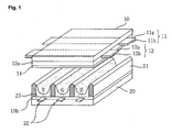
- a known plasma display panel has a front glass substrate 10 and a rear glass substrate 20.
- the front glass substrate 10 and the rear glass substrate 20 are coupled in parallel to each other with a predetermined distance therebetween.
- a sustaining electrode pair 11 and 12 for sustaining the light emission of a discharge cell is formed on the front glass substrate 10.
- the sustaining electrode pair 11 and 12 consists of a scan electrode 11 and sustain electrode 12.
- the scan electrode 11 is supplied with a scan pulse for scanning and a sustain pulse for sustaining discharging.
- the sustain electrode 12 is applied with a sustain pulse alternated with a sustain pulse applied to the scan electrode 11.
- the scan electrode 11 and the sustain electrode 12 are composed of transparent electrodes 11a and 12a made of transparent ITO material and bus electrodes 11 b and 12b made of metal, respectively.
- the sustaining electrode pair 11 and 12 are covered with a dielectric layer 13a.
- a protective layer 14 made of MgO is formed on the upper surface of the dielectric layer 13a so as to facilitate discharging more easily.
- a plurality of address electrodes 22 are arranged on the rear glass substrate 20 alternatively with the sustaining electrode pair 11 and 12.
- a dielectric layer 13b is formed on the address electrodes 22.
- Barrier ribs 21 for forming discharge cells are formed on the dielectric layer 13b.
- a phosphor 23 for emitting visible light is coated between the barrier ribs 21.
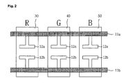
- the bus electrodes 11 a and 11 b are formed at upper and lower parts of a discharge cell 30 coated with R(red) phosphor, a discharge cell 40 coated with G(green) phosphor and a discharge cell 50 coated with B(blue) phosphor.
- the transparent electrodes 12a and 12b are formed in such a manner to be projected from the bus electrodes 11 a and 11 b toward the center of the discharge cell 30 coated with R(red) phosphor, of the discharge cell 40 coated with G(green) phosphor, and of the discharge cell 50 coated with B(blue) phosphor.
- the bus electrodes 11 a and 11 b and transparent electrodes 12a and 12b formed on the regions of each discharge cell have the same area.
- the amount of discharge is the same. Since the amount of discharge is the same in each discharge cell, the discharge efficiency in each discharge cell is significantly depending on the phosphor type.
- the emission efficiency of B phosphor is less than the emission efficiency of R phosphor or G phosphor. That is, the amount of light emitted from the B phosphor according to a specific amount of discharge is less than the amount of light emitted from the R phosphor or G phosphor. Therefore, if the area of the electrodes formed on each discharge cell is the same, the color temperature of an image displayed by the conventional plasma display panel is not being set to an appropriate level.
- an object of embodiments of the present invention is to address at least some of the problems and disadvantages of the background art.
- Embodiments of the present invention provide a plasma display panel comprising electrodes with an enhanced structure for improvement of color temperature.
- a plasma display panel comprising a first discharge cell provided with a first phosphor among a plurality of phosphors; a second discharge cell provided with a second phosphor among the plurality of phosphors; a first sustaining electrode pair formed on the first discharge cell and having a first area; and a second sustaining electrode pair formed on the second discharge cell and having a second area smaller than the first area.
- a plasma display panel comprising a first discharge cell partitioned by barrier ribs and provided with a first phosphor among a plurality of phosphors; a second discharge cell partitioned by barrier ribs and provided with a second phosphor among the plurality of phosphors; a first transparent electrode portion projected on the first discharge cell toward the center of the first discharge cell and having a first partial area; and a second transparent electrode portion projected on the second discharge cell toward the center of the second discharge cell and having a second partial area smaller than the first partial area.
- the color temperature of an image displayed by a plasma display panel is set to the appropriate level by enlarging the area of electrodes in the regions of a discharge cell provided with a specific phosphor.
- FIG.1 is a perspective view schematically showing a structure of a conventional plasma display panel
- FIG.2 shows an electrode structure of the conventional plasma display panel
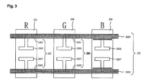
- FIG.3 is a plane view of a first embodiment of a plasma display panel.
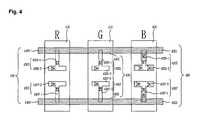
- FIG.4 is a plane view of a second embodiment of a plasma display panel.
- a first plasma display panel comprises a first discharge cell 300, a second discharge cell 310, a first sustaining electrode pair 320 and a second sustaining electrode pair 330.
- the first discharge cell 300 is partitioned by barrier ribs and provided with a first phosphor among a plurality of phosphors.
- the plurality of phosphor comprises a R (red) phosphor, a G (green) phosphor and a B (blue) phosphor.
- the first phosphor is a B phosphor.
- the second discharge cell 310 is partitioned by barrier ribs and provided with a second phosphor among a plurality of phosphors.
- the second phosphor is a R (red) phosphor or a G (green) phosphor.
- the first sustaining electrode pair 320 is formed on a front glass substrate (not shown) on the first discharge cell 300 and has a first area.
- Such first sustaining electrode pair 320 comprise a first scanning bus electrode 3201, a first sustaining bus electrode 3203, a first scanning transparent electrode 3205 and a first sustaining transparent electrode 3207.
- the position of the first scanning bus electrode 3201 and the first scanning transparent electrode 3205, and the position of the first sustaining bus electrode 3203 and the first sustaining transparent electrode 3207 can alternate with each other. That is, the first scanning bus electrode 3201 and the first scanning transparent electrode 3205 can be positioned at a lower part of the first discharge cell 300, and the first sustaining bus electrode 3203 and the first sustaining transparent electrode 3207 can be positioned at an upper part of the first discharge cell 300.
- the second sustaining electrode pair 330 is formed on a front glass substrate (not shown) on the second discharge cell 310 and has a second area smaller than the first area.
- Such second sustaining electrode pair 330 comprises a second scanning bus electrode 3301, a second sustaining bus electrode 3303, a second scanning transparent electrode 3305 and a second sustaining transparent electrode 3307.
- the position of the second scanning bus electrode 3301 and the second scanning transparent electrode 3305, and the position of the second sustaining bus electrode 3303 and of the second sustaining transparent electrode 3307 can alternate with each other.
- the second scanning bus electrode 3301 and the second scanning transparent electrode 3305 can be positioned at a lower part of the second discharge cell 310, and the second sustaining bus electrode 3303 and the second sustaining transparent electrode 3307 can be positioned at an upper part of the second discharge cell 310.
- the first scanning bus electrode 3201 and first sustaining bus electrode 3203 of the first sustaining electrode pair 320 is wider than the second scanning bus electrode 3301 and second sustaining bus electrode 3303 of the second sustaining electrode pair 330.
- the first scanning bus electrode 3201 and the first sustaining bus electrode 3203 are formed on the first discharge cell 300 where the B phosphor is formed
- the second scanning bus electrode 3301 and the second sustaining bus electrode 3303 are formed on the second discharge cell 310 where the R phosphor or G phosphor is formed
- the amount of discharge of the first discharge cell 300 becomes greater than the amount of discharge of the second discharge cell 310.
- the color temperature of an image displayed by the plasma display panel can be set to the appropriate level.
- a second plasma display panel comprises a first discharge cell 400, a second discharge cell 410, a first sustaining electrode pair 420 and a second sustaining electrode pair 430.
- the first discharge cell 400 is partitioned by barrier ribs and provided with a first phosphor among a plurality of phosphors.
- the plurality of phosphor comprises a R(red) phosphor, a G(green) phosphor and a B(blue) phosphor.
- the first phosphor is a B phosphor.
- the second discharge cell 410 is partitioned by barrier ribs and provided with a second phosphor among a plurality of phosphors.
- the second phosphor is a R(red) phosphor or G(green) phosphor.
- the first sustaining electrode pair 420 is formed on a front glass substrate (not shown) on the first discharge cell 400 and has a first area.
- Such first sustaining electrode pair 420 comprise a first scanning bus electrode 4201, a first sustaining bus electrode 4203, a first scanning transparent electrode 4205 and a first sustaining transparent electrode 4207.
- the position of the first scanning bus electrode 4201 and the first scanning transparent electrode 4205, and the position of the first sustaining bus electrode 4203 and of the first sustaining transparent electrode 4207 can alternate with each other.
- the first scanning bus electrode 4201 and the first scanning transparent electrode 4205 can be positioned at a lower part of the first discharge cell 400, and the first sustaining bus electrode 4203 and the first sustaining transparent electrode 4207 can be positioned at an upper part of the first discharge cell 400.
- the first scanning transparent electrode 4205 and the first sustaining transparent electrode 4207 are projected from the first scanning bus electrode 4201 and the first sustaining bus electrode 4203, respectively, toward the center of the first discharge cell 400.
- the first scanning transparent electrode 4205 and the first sustaining transparent electrode 4207 have a first partial area. That is, the first partial area is the sum of the areas of the first scanning transparent electrode 4205 and first sustaining transparent electrode 4207.
- the first scanning transparent electrode 4205 comprises a first scanning vertical connecting portion 4205-1 vertically connecting to the first scanning bus electrode 4201 and a first scanning horizontal connecting portion 4205-2 vertically connecting to the first scanning vertical connecting portion 4205-1.
- the first sustaining transparent electrode 4207 comprises a first sustaining vertical connecting portion 4207-1 vertically connecting to the first sustaining bus electrode 4203 and a first sustaining horizontal connecting portion 4207-2 vertically connecting to the first sustaining vertical connecting portion 4207-1.
- the second sustaining electrode pair 430 is formed on a front glass substrate (not shown) on the second discharge cell 410 and has a second area smaller than the first area.
- Such second sustaining electrode pair 430 comprises a second scanning bus electrode 4301, a second sustaining bus electrode 4303, a second scanning transparent electrode 4305 and a second sustaining transparent electrode 4307.
- the position of the second scanning bus electrode 4301 and the second scanning transparent electrode 4305, and the position of the second sustaining bus electrode 4303 and of the second sustaining transparent electrode 4307 can be alternate with each other.
- the second scanning bus electrode 4301 and the second scanning transparent electrode 4305 can be positioned at a lower part of the second discharge cell 410, and the second sustaining bus electrode 3303 and the second sustaining transparent electrode 4307 can be positioned at an upper part of the second discharge cell 410.
- the second scanning transparent electrode 4305 and the second sustaining transparent electrode 4307 are projected from the second scanning bus electrode 4201 and the second sustaining bus electrode 4303, respectively, toward the center of the second discharge cell 410.
- the second scanning transparent electrode 4305 and the second sustaining transparent electrode 4307 have a second partial area. That is, the second partial area is the sum of the areas of the second scanning transparent electrode 4305 and second sustaining transparent electrode 4307.
- the second scanning transparent electrode 4305 comprises a second scanning vertical connecting portion 4305-1 vertically connecting to the second scanning bus electrode 4301 and a second scanning horizontal connecting portion 4305-2 vertically connecting to the second scanning vertical connecting portion 4205-1.
- the second sustaining transparent electrode 4307 comprises a second sustaining vertical connecting portion 4307-1 vertically connecting to the second sustaining bus electrode 4303 and a second sustaining horizontal connecting portion 4307-2 vertically connecting to the second sustaining vertical connecting portion 4307-1.
- the first partial area of the first scanning transparent electrode 4205 and the first sustaining transparent electrode 4207 is larger than the second area of the second scanning transparent electrode 4305 and second sustaining transparent electrode 4307.
- the first scanning transparent electrode 4205 and the first sustaining transparent electrode 4207 are formed on the first discharge cell 400 where the B phosphor is formed
- the second scanning transparent electrode 4305 and the second sustaining transparent electrode 4307 are formed on the second discharge cell 410 where the R phosphor or G phosphor is formed
- the amount of discharge of the first discharge cell 400 becomes greater than the amount of discharge of the second discharge cell 410.
- the width w1 of the first scanning vertical connecting portion 4205-1 of the first scanning transparent electrode 4205 can be wider than the width w2 of the second scanning vertical connecting portion 4305-1 of the second scanning transparent electrode 4305.
- the width w3 of the first scanning horizontal connecting portion 4305-2 of the second scanning transparent electrode 4305 can be wider than the width w4 of the second scanning horizontal connecting portion 4305-2 of the second scanning transparent electrode 4305.
- the width w6 of the first sustaining vertical connecting portion 4207-1 of the first sustaining transparent electrode 4207 can be wider than the width w5 of the second sustaining vertical connecting portion 4307-1 of the second sustaining transparent electrode 4307.
- the width w7 of the first sustaining horizontal connecting portion 4207-1 of the first sustaining transparent 4207 can be wider than the width w8 of the second sustaining horizontal connecting portion 4307-2 of the second sustaining transparent electrode 4307.
- first scanning horizontal connecting portion 4205-2 and first sustaining horizontal connecting portion 4207-2 increase toward the center of the first discharge cell 400, a discharge gap is reduced and thus a discharge firing voltage increases.
- the first scanning horizontal connecting portion 4205-2 and the first sustaining horizontal connecting portion 4207-2 have a width that increases toward the barrier ribs, respectively.
Landscapes
- Engineering & Computer Science (AREA)
- Physics & Mathematics (AREA)
- Plasma & Fusion (AREA)
- Chemical & Material Sciences (AREA)
- Materials Engineering (AREA)
- Gas-Filled Discharge Tubes (AREA)
Abstract
Description
- The present invention relates to a plasma display panel. Embodiments relate to a plasma display panel comprising scanning bus electrodes and sustaining bus electrodes formed on R, G and B cells.
- In a conventional plasma display panel, a barrier rib formed between front and rear substrates made of soda-lime glass constitutes one unit cells, Each cell is filled with an inert gas such as helium-xenon (He-Xe), helium-neon (He-Ne), etc., If the inert gas is discharged with a high frequency voltage, vacuum ultraviolet rays are generated. Phosphor formed between the barrier ribs emits light corresponding to images.
- Referring to FIG.1, a known plasma display panel has a
front glass substrate 10 and arear glass substrate 20. Thefront glass substrate 10 and therear glass substrate 20 are coupled in parallel to each other with a predetermined distance therebetween. - A
sustaining electrode pair front glass substrate 10. The sustainingelectrode pair scan electrode 11 and sustainelectrode 12. Thescan electrode 11 is supplied with a scan pulse for scanning and a sustain pulse for sustaining discharging. Thesustain electrode 12 is applied with a sustain pulse alternated with a sustain pulse applied to thescan electrode 11. Thescan electrode 11 and thesustain electrode 12 are composed oftransparent electrodes bus electrodes sustaining electrode pair dielectric layer 13a. Aprotective layer 14 made of MgO is formed on the upper surface of thedielectric layer 13a so as to facilitate discharging more easily. - A plurality of
address electrodes 22 are arranged on therear glass substrate 20 alternatively with thesustaining electrode pair dielectric layer 13b is formed on theaddress electrodes 22. Barrier ribs 21 for forming discharge cells are formed on thedielectric layer 13b. Aphosphor 23 for emitting visible light is coated between thebarrier ribs 21. - Turning to FIG.2, the
bus electrodes discharge cell 30 coated with R(red) phosphor, adischarge cell 40 coated with G(green) phosphor and adischarge cell 50 coated with B(blue) phosphor. Thetransparent electrodes bus electrodes discharge cell 30 coated with R(red) phosphor, of thedischarge cell 40 coated with G(green) phosphor, and of thedischarge cell 50 coated with B(blue) phosphor. - The
bus electrodes transparent electrodes - Accordingly, an object of embodiments of the present invention is to address at least some of the problems and disadvantages of the background art.
- Embodiments of the present invention provide a plasma display panel comprising electrodes with an enhanced structure for improvement of color temperature.
- In one aspect there is provided a plasma display panel comprising a first discharge cell provided with a first phosphor among a plurality of phosphors; a second discharge cell provided with a second phosphor among the plurality of phosphors; a first sustaining electrode pair formed on the first discharge cell and having a first area; and a second sustaining electrode pair formed on the second discharge cell and having a second area smaller than the first area.
- In another aspect there is provided a plasma display panel comprising a first discharge cell partitioned by barrier ribs and provided with a first phosphor among a plurality of phosphors; a second discharge cell partitioned by barrier ribs and provided with a second phosphor among the plurality of phosphors; a first transparent electrode portion projected on the first discharge cell toward the center of the first discharge cell and having a first partial area; and a second transparent electrode portion projected on the second discharge cell toward the center of the second discharge cell and having a second partial area smaller than the first partial area.
- Features of embodiments are defined in the appended claims.
- In embodiments, the color temperature of an image displayed by a plasma display panel is set to the appropriate level by enlarging the area of electrodes in the regions of a discharge cell provided with a specific phosphor.
- The invention will be more clearly understood after reading the following description together with the accompanying drawings, in which:
- FIG.1 is a perspective view schematically showing a structure of a conventional plasma display panel;
- FIG.2 shows an electrode structure of the conventional plasma display panel;
- FIG.3 is a plane view of a first embodiment of a plasma display panel; and
- FIG.4 is a plane view of a second embodiment of a plasma display panel.
- <Embodiment 1>
- As shown in FIG.3, a first plasma display panel comprises a
first discharge cell 300, asecond discharge cell 310, a firstsustaining electrode pair 320 and a secondsustaining electrode pair 330. - The
first discharge cell 300 is partitioned by barrier ribs and provided with a first phosphor among a plurality of phosphors. In this embodiment the plurality of phosphor comprises a R (red) phosphor, a G (green) phosphor and a B (blue) phosphor. Again in this embodiment, the first phosphor is a B phosphor. - The
second discharge cell 310 is partitioned by barrier ribs and provided with a second phosphor among a plurality of phosphors. In this embodiment, the second phosphor is a R (red) phosphor or a G (green) phosphor. - The first
sustaining electrode pair 320 is formed on a front glass substrate (not shown) on thefirst discharge cell 300 and has a first area. Such firstsustaining electrode pair 320 comprise a firstscanning bus electrode 3201, a firstsustaining bus electrode 3203, a first scanningtransparent electrode 3205 and a first sustainingtransparent electrode 3207. The position of the firstscanning bus electrode 3201 and the first scanningtransparent electrode 3205, and the position of the firstsustaining bus electrode 3203 and the first sustainingtransparent electrode 3207 can alternate with each other. That is, the firstscanning bus electrode 3201 and the first scanningtransparent electrode 3205 can be positioned at a lower part of thefirst discharge cell 300, and the first sustainingbus electrode 3203 and the first sustainingtransparent electrode 3207 can be positioned at an upper part of thefirst discharge cell 300. - The second
sustaining electrode pair 330 is formed on a front glass substrate (not shown) on thesecond discharge cell 310 and has a second area smaller than the first area. Such secondsustaining electrode pair 330 comprises a secondscanning bus electrode 3301, a secondsustaining bus electrode 3303, a second scanningtransparent electrode 3305 and a second sustainingtransparent electrode 3307. The position of the secondscanning bus electrode 3301 and the second scanningtransparent electrode 3305, and the position of the second sustainingbus electrode 3303 and of the second sustainingtransparent electrode 3307 can alternate with each other. That is, the secondscanning bus electrode 3301 and the second scanningtransparent electrode 3305 can be positioned at a lower part of thesecond discharge cell 310, and the second sustainingbus electrode 3303 and the second sustainingtransparent electrode 3307 can be positioned at an upper part of thesecond discharge cell 310. - As shown in FIG.3, the first
scanning bus electrode 3201 and first sustainingbus electrode 3203 of the first sustainingelectrode pair 320 is wider than the secondscanning bus electrode 3301 and second sustainingbus electrode 3303 of the secondsustaining electrode pair 330. As a result, as the firstscanning bus electrode 3201 and the first sustainingbus electrode 3203 are formed on thefirst discharge cell 300 where the B phosphor is formed, and the secondscanning bus electrode 3301 and the second sustainingbus electrode 3303 are formed on thesecond discharge cell 310 where the R phosphor or G phosphor is formed, the amount of discharge of thefirst discharge cell 300 becomes greater than the amount of discharge of thesecond discharge cell 310. Therefore, because the first discharge cell in which the B phosphor having a smaller light emission efficiency is formed, emits a greater amount of light than an amount of light emitted by the second discharge cell, the color temperature of an image displayed by the plasma display panel can be set to the appropriate level. - <Embodiment 2>
- As shown in FIG.4, a second plasma display panel comprises a
first discharge cell 400, asecond discharge cell 410, a firstsustaining electrode pair 420 and a secondsustaining electrode pair 430. - The
first discharge cell 400 is partitioned by barrier ribs and provided with a first phosphor among a plurality of phosphors. In this embodiment the plurality of phosphor comprises a R(red) phosphor, a G(green) phosphor and a B(blue) phosphor. Again in this embodiment, the first phosphor is a B phosphor. - The
second discharge cell 410 is partitioned by barrier ribs and provided with a second phosphor among a plurality of phosphors. In this embodiment, the second phosphor is a R(red) phosphor or G(green) phosphor. - The first
sustaining electrode pair 420 is formed on a front glass substrate (not shown) on thefirst discharge cell 400 and has a first area. Such firstsustaining electrode pair 420 comprise a firstscanning bus electrode 4201, a firstsustaining bus electrode 4203, a first scanningtransparent electrode 4205 and a first sustainingtransparent electrode 4207. The position of the firstscanning bus electrode 4201 and the first scanningtransparent electrode 4205, and the position of the firstsustaining bus electrode 4203 and of the first sustainingtransparent electrode 4207 can alternate with each other. That is, the firstscanning bus electrode 4201 and the first scanningtransparent electrode 4205 can be positioned at a lower part of thefirst discharge cell 400, and the first sustainingbus electrode 4203 and the first sustainingtransparent electrode 4207 can be positioned at an upper part of thefirst discharge cell 400. The first scanningtransparent electrode 4205 and the first sustainingtransparent electrode 4207 are projected from the firstscanning bus electrode 4201 and the first sustainingbus electrode 4203, respectively, toward the center of thefirst discharge cell 400. The first scanningtransparent electrode 4205 and the first sustainingtransparent electrode 4207 have a first partial area. That is, the first partial area is the sum of the areas of the first scanningtransparent electrode 4205 and first sustainingtransparent electrode 4207. The first scanningtransparent electrode 4205 comprises a first scanning vertical connecting portion 4205-1 vertically connecting to the firstscanning bus electrode 4201 and a first scanning horizontal connecting portion 4205-2 vertically connecting to the first scanning vertical connecting portion 4205-1. The first sustainingtransparent electrode 4207 comprises a first sustaining vertical connecting portion 4207-1 vertically connecting to the first sustainingbus electrode 4203 and a first sustaining horizontal connecting portion 4207-2 vertically connecting to the first sustaining vertical connecting portion 4207-1. - The second sustaining
electrode pair 430 is formed on a front glass substrate (not shown) on thesecond discharge cell 410 and has a second area smaller than the first area. Such second sustainingelectrode pair 430 comprises a secondscanning bus electrode 4301, a second sustainingbus electrode 4303, a second scanningtransparent electrode 4305 and a second sustainingtransparent electrode 4307. The position of the secondscanning bus electrode 4301 and the second scanningtransparent electrode 4305, and the position of the second sustainingbus electrode 4303 and of the second sustainingtransparent electrode 4307 can be alternate with each other. That is, the secondscanning bus electrode 4301 and the second scanningtransparent electrode 4305 can be positioned at a lower part of thesecond discharge cell 410, and the second sustainingbus electrode 3303 and the second sustainingtransparent electrode 4307 can be positioned at an upper part of thesecond discharge cell 410. The second scanningtransparent electrode 4305 and the second sustainingtransparent electrode 4307 are projected from the secondscanning bus electrode 4201 and the second sustainingbus electrode 4303, respectively, toward the center of thesecond discharge cell 410. The second scanningtransparent electrode 4305 and the second sustainingtransparent electrode 4307 have a second partial area. That is, the second partial area is the sum of the areas of the second scanningtransparent electrode 4305 and second sustainingtransparent electrode 4307. The second scanningtransparent electrode 4305 comprises a second scanning vertical connecting portion 4305-1 vertically connecting to the secondscanning bus electrode 4301 and a second scanning horizontal connecting portion 4305-2 vertically connecting to the second scanning vertical connecting portion 4205-1. The second sustainingtransparent electrode 4307 comprises a second sustaining vertical connecting portion 4307-1 vertically connecting to the second sustainingbus electrode 4303 and a second sustaining horizontal connecting portion 4307-2 vertically connecting to the second sustaining vertical connecting portion 4307-1. - As shown in FIG.4, the first partial area of the first scanning
transparent electrode 4205 and the first sustainingtransparent electrode 4207 is larger than the second area of the second scanningtransparent electrode 4305 and second sustainingtransparent electrode 4307. As a result, as the first scanningtransparent electrode 4205 and the first sustainingtransparent electrode 4207 are formed on thefirst discharge cell 400 where the B phosphor is formed, and the second scanningtransparent electrode 4305 and the second sustainingtransparent electrode 4307 are formed on thesecond discharge cell 410 where the R phosphor or G phosphor is formed, the amount of discharge of thefirst discharge cell 400 becomes greater than the amount of discharge of thesecond discharge cell 410. Therefore, because the B phosphor having a lower light emission efficiency emits a greater amount of light, the color temperature of an image displayed by the plasma display panel can be set to the appropriate level. The width w1 of the first scanning vertical connecting portion 4205-1 of the first scanningtransparent electrode 4205 can be wider than the width w2 of the second scanning vertical connecting portion 4305-1 of the second scanningtransparent electrode 4305. The width w3 of the first scanning horizontal connecting portion 4305-2 of the second scanningtransparent electrode 4305 can be wider than the width w4 of the second scanning horizontal connecting portion 4305-2 of the second scanningtransparent electrode 4305. Likewise, the width w6 of the first sustaining vertical connecting portion 4207-1 of the first sustainingtransparent electrode 4207 can be wider than the width w5 of the second sustaining vertical connecting portion 4307-1 of the second sustainingtransparent electrode 4307. The width w7 of the first sustaining horizontal connecting portion 4207-1 of the first sustaining transparent 4207 can be wider than the width w8 of the second sustaining horizontal connecting portion 4307-2 of the second sustainingtransparent electrode 4307. - If the width of the first scanning horizontal connecting portion 4205-2 and first sustaining horizontal connecting portion 4207-2 increases toward the center of the
first discharge cell 400, a discharge gap is reduced and thus a discharge firing voltage increases. As a result, in this embodiment the first scanning horizontal connecting portion 4205-2 and the first sustaining horizontal connecting portion 4207-2 have a width that increases toward the barrier ribs, respectively. - An embodiment of the invention being thus described, it will be obvious that the same may be varied in many ways, Such variations are not to be regarded as a departure from the scope of the invention which is limited only by the extent of the following claims.
Claims (13)
- A plasma display panel, comprising:a first discharge cell comprising first phosphor among a plurality of phosphors is formed;a second discharge cell comprising second phosphor among the plurality of phosphors is formed;a first sustaining electrode pair formed on the first discharge cell and having a first area; anda second sustaining electrode pair formed on the second discharge cell and having a second area smaller than the first area.
- The plasma display panel as claimed in claim 1, wherein the first sustaining electrode pair comprises a first scanning bus electrode, the second sustaining electrode pair comprises a second scanning bus electrode, and the first scanning bus electrode is wider than the second scanning bus electrode.
- The plasma display panel as claimed in claim 1, wherein the first sustaining electrode pair comprises a first sustaining bus electrode, the second sustaining electrode pair comprises a second sustaining bus electrode, and the first sustaining bus electrode is wider than the second scanning bus electrode.
- A plasma display panel, comprising:a first discharge cell partitioned by barrier ribs and comprising first phosphor among a plurality of phosphors is formed;a second discharge cell partitioned by barrier ribs and provided with a second phosphor among the plurality of phosphors is formed;a first transparent electrode portion projected on the first discharge cell toward the center of the first discharge cell and having a first partial area; anda second transparent electrode portion projected on the second discharge cell toward the center of the second discharge cell and having a second partial area smaller than the first partial area.
- The plasma display panel as claimed in claim 1 or 4, wherein the first phosphor is a blue phosphor.
- The plasma display panel as claimed in claim 4, wherein the first transparent electrode portion comprises a first scanning vertical connecting portion formed toward the center of the first discharge cell, the second transparent electrode portion comprises a second scanning vertical connecting portion formed toward the center of the second discharge cell, and the first scan vertical connecting portion is wider than the second scanning vertical connecting portion.
- The plasma display panel as claimed in claim 6, wherein the first scanning vertical connecting portion is wider than the second scanning vertical connecting portion, and the width of the first scanning vertical connecting portion increases in the direction of the barrier ribs partitioning the first discharge cell.
- The plasma display panel as claimed in claim 6, wherein the first transparent electrode portion further comprises a first scanning horizontal connecting portion connecting to the first scanning vertical connecting portion, the second transparent electrode portion further comprises a second scanning horizontal connecting portion connecting to the second scanning vertical connecting portion, and the first scanning horizontal connecting portion is wider than the second scanning horizontal connecting portion.
- The plasma display panel as claimed in claim 8, wherein the first scanning horizontal connecting portion is wider than the second scanning horizontal connecting portion, and the width of the first scanning horizontal connecting portion increases in the direction of the barrier ribs partitioning the first discharge cell.
- The plasma display panel as claimed in claim 4, wherein the first transparent electrode portion comprises a first sustaining vertical connecting portion formed toward the center of the first discharge cell, the second transparent electrode portion comprises a second sustaining vertical connecting portion formed toward the center of the second discharge cell, and the first sustaining vertical connecting portion is wider than the second sustaining vertical connecting portion.
- The plasma display panel as claimed in claim 10, wherein the first sustaining vertical connecting portion is wider than the second sustaining vertical connecting portion, and the width of the first sustaining vertical connecting portion increases in the direction of the barrier ribs partitioning the first discharge cell.
- The plasma display panel as claimed in claim 10, wherein the first transparent electrode portion further comprises a first sustaining horizontal connecting portion connecting to the first sustaining vertical connecting portion, the second transparent electrode portion further comprises a second sustaining horizontal connecting portion connecting to the second sustaining vertical connecting portion, and the first sustaining horizontal connecting portion is wider than the second sustaining horizontal connecting portion.
- The plasma display panel as claimed in claim 12, wherein the first sustaining horizontal connecting portion is wider than the second sustaining horizontal connecting portion, and the width of the first sustaining horizontal connecting portion increases in the direction of the barrier ribs partitioning the first discharge cell.
Applications Claiming Priority (1)
| Application Number | Priority Date | Filing Date | Title |
|---|---|---|---|
| KR1020040080640A KR20060031560A (en) | 2004-10-08 | 2004-10-08 | Plasma display panel including scan electrode and sustain electrode |
Publications (2)
| Publication Number | Publication Date |
|---|---|
| EP1646064A2 true EP1646064A2 (en) | 2006-04-12 |
| EP1646064A3 EP1646064A3 (en) | 2007-12-05 |
Family
ID=36144564
Family Applications (1)
| Application Number | Title | Priority Date | Filing Date |
|---|---|---|---|
| EP05256270A Pending EP1646064A3 (en) | 2004-10-08 | 2005-10-07 | Plasma display panel |
Country Status (5)
| Country | Link |
|---|---|
| US (1) | US20060076875A1 (en) |
| EP (1) | EP1646064A3 (en) |
| JP (1) | JP2006108111A (en) |
| KR (1) | KR20060031560A (en) |
| CN (1) | CN1758408A (en) |
Families Citing this family (1)
| Publication number | Priority date | Publication date | Assignee | Title |
|---|---|---|---|---|
| JP2008027608A (en) * | 2006-07-18 | 2008-02-07 | Advanced Pdp Development Corp | Plasma display panel |
Family Cites Families (15)
| Publication number | Priority date | Publication date | Assignee | Title |
|---|---|---|---|---|
| JPH11306996A (en) * | 1998-02-23 | 1999-11-05 | Mitsubishi Electric Corp | Surface discharge type plasma display device, surface discharge type plasma display panel, and substrate for surface discharge type plasma display panel |
| JP3410024B2 (en) * | 1998-06-18 | 2003-05-26 | 富士通株式会社 | Gas discharge display |
| JP3329285B2 (en) * | 1998-10-16 | 2002-09-30 | 日本電気株式会社 | Color plasma display panel |
| JP3864204B2 (en) * | 1999-02-19 | 2006-12-27 | 株式会社日立プラズマパテントライセンシング | Plasma display panel |
| JP3589892B2 (en) * | 1999-03-18 | 2004-11-17 | 富士通株式会社 | Plasma display panel |
| JP2001160361A (en) * | 1999-09-21 | 2001-06-12 | Mitsubishi Electric Corp | Plasma display panel substrate and plasma display panel |
| JP3790075B2 (en) * | 1999-10-27 | 2006-06-28 | パイオニア株式会社 | Plasma display panel |
| JP3587118B2 (en) * | 2000-02-24 | 2004-11-10 | 日本電気株式会社 | Plasma display panel |
| JP2002056781A (en) * | 2000-05-31 | 2002-02-22 | Mitsubishi Electric Corp | Plasma display panel and plasma display device |
| KR100408213B1 (en) * | 2000-06-26 | 2003-12-01 | 황기웅 | an AC plasma display panel having delta color pixels of closed shape subpixels |
| JP4527862B2 (en) * | 2000-09-04 | 2010-08-18 | 日立プラズマディスプレイ株式会社 | Plasma display panel |
| US6853136B2 (en) * | 2001-08-20 | 2005-02-08 | Samsung Sdi Co., Ltd. | Plasma display panel having delta discharge cell arrangement |
| US6940224B2 (en) * | 2002-01-10 | 2005-09-06 | Lg Electronics Inc. | Plasma display panel having specifically spaced holes formed in the electrodes |
| TW564456B (en) * | 2002-06-27 | 2003-12-01 | Chunghwa Picture Tubes Ltd | Electrode structure with white balance adjusting |
| KR100520831B1 (en) * | 2003-08-08 | 2005-10-12 | 엘지전자 주식회사 | Plasma display panel |
-
2004
- 2004-10-08 KR KR1020040080640A patent/KR20060031560A/en not_active Withdrawn
-
2005
- 2005-10-06 US US11/244,169 patent/US20060076875A1/en not_active Abandoned
- 2005-10-07 EP EP05256270A patent/EP1646064A3/en active Pending
- 2005-10-08 CN CNA2005101134061A patent/CN1758408A/en active Pending
- 2005-10-11 JP JP2005296118A patent/JP2006108111A/en active Pending
Also Published As
| Publication number | Publication date |
|---|---|
| US20060076875A1 (en) | 2006-04-13 |
| JP2006108111A (en) | 2006-04-20 |
| KR20060031560A (en) | 2006-04-12 |
| CN1758408A (en) | 2006-04-12 |
| EP1646064A3 (en) | 2007-12-05 |
Similar Documents
| Publication | Publication Date | Title |
|---|---|---|
| US20070205722A1 (en) | Plasma display panel | |
| US6392344B1 (en) | Plasma display device | |
| US7486022B2 (en) | Plasma display panel (PDP) | |
| US7135819B2 (en) | Plasma display panel | |
| EP1646064A2 (en) | Plasma display panel | |
| US7187126B2 (en) | Plasma display panel including metal electrodes formed on transparent electrodes | |
| EP1646065A2 (en) | Plasma display panel and plasma display apparatus comprising electrodes | |
| KR100613013B1 (en) | Plasma display panel | |
| US7411348B2 (en) | Plasma display panel | |
| US7420329B2 (en) | Plasma display panel (PDP) | |
| US20060197450A1 (en) | Dielectric layer structure and plasma display panel having the same | |
| KR100738213B1 (en) | Plasma display panel | |
| KR100717786B1 (en) | Plasma display panel | |
| KR100719000B1 (en) | Plasma display panel | |
| KR100667590B1 (en) | Plasma display panel | |
| KR100499080B1 (en) | Plasma display panel | |
| KR100496254B1 (en) | Plasma display panel | |
| KR100670316B1 (en) | Plasma display panel | |
| KR20000066410A (en) | Plasma display panel | |
| KR20050117222A (en) | Plasma display panel | |
| KR20050104190A (en) | Plasma display panel | |
| KR20060019151A (en) | Plasma display panel | |
| EP1646066A2 (en) | Plasma display panel and plasma display apparatus comprising electrodes | |
| KR20060010296A (en) | Plasma display panel | |
| KR20060087634A (en) | Plasma display panel |
Legal Events
| Date | Code | Title | Description |
|---|---|---|---|
| PUAI | Public reference made under article 153(3) epc to a published international application that has entered the european phase |
Free format text: ORIGINAL CODE: 0009012 |
|
| 17P | Request for examination filed |
Effective date: 20051019 |
|
| AK | Designated contracting states |
Kind code of ref document: A2 Designated state(s): AT BE BG CH CY CZ DE DK EE ES FI FR GB GR HU IE IS IT LI LT LU LV MC NL PL PT RO SE SI SK TR |
|
| AX | Request for extension of the european patent |
Extension state: AL BA HR MK YU |
|
| PUAL | Search report despatched |
Free format text: ORIGINAL CODE: 0009013 |
|
| AK | Designated contracting states |
Kind code of ref document: A3 Designated state(s): AT BE BG CH CY CZ DE DK EE ES FI FR GB GR HU IE IS IT LI LT LU LV MC NL PL PT RO SE SI SK TR |
|
| AX | Request for extension of the european patent |
Extension state: AL BA HR MK YU |
|
| STAA | Information on the status of an ep patent application or granted ep patent |
Free format text: STATUS: EXAMINATION IS IN PROGRESS |
|
| 17Q | First examination report despatched |
Effective date: 20080703 |
|
| AKX | Designation fees paid |
Designated state(s): DE FR GB NL |