EP1639411B1 - A nano impression lithographic process which involves the use of a die having a region able to generate heat - Google Patents
A nano impression lithographic process which involves the use of a die having a region able to generate heat Download PDFInfo
- Publication number
- EP1639411B1 EP1639411B1 EP04743806A EP04743806A EP1639411B1 EP 1639411 B1 EP1639411 B1 EP 1639411B1 EP 04743806 A EP04743806 A EP 04743806A EP 04743806 A EP04743806 A EP 04743806A EP 1639411 B1 EP1639411 B1 EP 1639411B1
- Authority
- EP
- European Patent Office
- Prior art keywords
- process according
- die
- polymeric material
- mass
- region
- Prior art date
- Legal status (The legal status is an assumption and is not a legal conclusion. Google has not performed a legal analysis and makes no representation as to the accuracy of the status listed.)
- Expired - Lifetime
Links
- 238000000034 method Methods 0.000 title claims abstract description 81
- 230000008569 process Effects 0.000 title claims abstract description 73
- 239000000463 material Substances 0.000 claims abstract description 60
- 238000010438 heat treatment Methods 0.000 claims abstract description 21
- 230000002123 temporal effect Effects 0.000 claims abstract 2
- 239000010410 layer Substances 0.000 claims description 40
- 239000000758 substrate Substances 0.000 claims description 17
- 239000010703 silicon Substances 0.000 claims description 11
- 229910052710 silicon Inorganic materials 0.000 claims description 11
- 239000010408 film Substances 0.000 claims description 9
- 239000002344 surface layer Substances 0.000 claims description 9
- 239000004020 conductor Substances 0.000 claims description 7
- 229910052759 nickel Inorganic materials 0.000 claims description 7
- 239000002184 metal Substances 0.000 claims description 6
- 229910052751 metal Inorganic materials 0.000 claims description 6
- 229920001169 thermoplastic Polymers 0.000 claims description 6
- 239000004416 thermosoftening plastic Substances 0.000 claims description 6
- 239000003795 chemical substances by application Substances 0.000 claims description 5
- 229920001483 poly(ethyl methacrylate) polymer Polymers 0.000 claims description 5
- 229920003229 poly(methyl methacrylate) Polymers 0.000 claims description 5
- 230000009477 glass transition Effects 0.000 claims description 4
- 238000005468 ion implantation Methods 0.000 claims description 4
- 239000004065 semiconductor Substances 0.000 claims description 4
- 238000000926 separation method Methods 0.000 claims description 4
- 239000010409 thin film Substances 0.000 claims description 4
- 239000011521 glass Substances 0.000 claims description 3
- 239000000203 mixture Substances 0.000 claims description 3
- -1 polyethylene terephthalates Polymers 0.000 claims description 3
- 206010068150 Acoustic shock Diseases 0.000 claims description 2
- 229910045601 alloy Inorganic materials 0.000 claims description 2
- 239000000956 alloy Substances 0.000 claims description 2
- 229910052804 chromium Inorganic materials 0.000 claims description 2
- 229910052802 copper Inorganic materials 0.000 claims description 2
- 238000007373 indentation Methods 0.000 claims description 2
- 229910052741 iridium Inorganic materials 0.000 claims description 2
- 229910052750 molybdenum Inorganic materials 0.000 claims description 2
- 229920000515 polycarbonate Polymers 0.000 claims description 2
- 239000004417 polycarbonate Substances 0.000 claims description 2
- 229920000139 polyethylene terephthalate Polymers 0.000 claims description 2
- 229920000098 polyolefin Polymers 0.000 claims description 2
- 229910052709 silver Inorganic materials 0.000 claims description 2
- 229910052719 titanium Inorganic materials 0.000 claims description 2
- 229910052720 vanadium Inorganic materials 0.000 claims description 2
- 239000012212 insulator Substances 0.000 claims 1
- 229920001707 polybutylene terephthalate Polymers 0.000 claims 1
- 230000001360 synchronised effect Effects 0.000 claims 1
- PXHVJJICTQNCMI-UHFFFAOYSA-N nickel Substances [Ni] PXHVJJICTQNCMI-UHFFFAOYSA-N 0.000 description 11
- VYPSYNLAJGMNEJ-UHFFFAOYSA-N Silicium dioxide Chemical compound O=[Si]=O VYPSYNLAJGMNEJ-UHFFFAOYSA-N 0.000 description 10
- 239000012815 thermoplastic material Substances 0.000 description 10
- XUIMIQQOPSSXEZ-UHFFFAOYSA-N Silicon Chemical compound [Si] XUIMIQQOPSSXEZ-UHFFFAOYSA-N 0.000 description 9
- 238000004519 manufacturing process Methods 0.000 description 7
- 230000008901 benefit Effects 0.000 description 5
- 230000000694 effects Effects 0.000 description 4
- 238000005516 engineering process Methods 0.000 description 4
- 229920002120 photoresistant polymer Polymers 0.000 description 4
- 229910052814 silicon oxide Inorganic materials 0.000 description 4
- 238000001816 cooling Methods 0.000 description 3
- 150000002500 ions Chemical class 0.000 description 3
- 238000004377 microelectronic Methods 0.000 description 3
- 238000001020 plasma etching Methods 0.000 description 3
- 239000004926 polymethyl methacrylate Substances 0.000 description 3
- 238000003825 pressing Methods 0.000 description 3
- 238000007639 printing Methods 0.000 description 3
- 230000009467 reduction Effects 0.000 description 3
- 235000012239 silicon dioxide Nutrition 0.000 description 3
- VYZAMTAEIAYCRO-UHFFFAOYSA-N Chromium Chemical compound [Cr] VYZAMTAEIAYCRO-UHFFFAOYSA-N 0.000 description 2
- 239000003990 capacitor Substances 0.000 description 2
- 239000000919 ceramic Substances 0.000 description 2
- 238000000151 deposition Methods 0.000 description 2
- 230000008021 deposition Effects 0.000 description 2
- 230000005670 electromagnetic radiation Effects 0.000 description 2
- 238000009713 electroplating Methods 0.000 description 2
- 239000010931 gold Substances 0.000 description 2
- 239000007788 liquid Substances 0.000 description 2
- 238000001459 lithography Methods 0.000 description 2
- 238000001000 micrograph Methods 0.000 description 2
- 238000000206 photolithography Methods 0.000 description 2
- 229920000642 polymer Polymers 0.000 description 2
- 239000010453 quartz Substances 0.000 description 2
- 229910052594 sapphire Inorganic materials 0.000 description 2
- 239000010980 sapphire Substances 0.000 description 2
- HBMJWWWQQXIZIP-UHFFFAOYSA-N silicon carbide Chemical compound [Si+]#[C-] HBMJWWWQQXIZIP-UHFFFAOYSA-N 0.000 description 2
- 229910010271 silicon carbide Inorganic materials 0.000 description 2
- 239000000377 silicon dioxide Substances 0.000 description 2
- 229910052581 Si3N4 Inorganic materials 0.000 description 1
- 230000009471 action Effects 0.000 description 1
- 230000004888 barrier function Effects 0.000 description 1
- 230000015572 biosynthetic process Effects 0.000 description 1
- 229910052681 coesite Inorganic materials 0.000 description 1
- 230000008602 contraction Effects 0.000 description 1
- 238000007796 conventional method Methods 0.000 description 1
- 229910052906 cristobalite Inorganic materials 0.000 description 1
- 229910021419 crystalline silicon Inorganic materials 0.000 description 1
- 230000007423 decrease Effects 0.000 description 1
- 230000001419 dependent effect Effects 0.000 description 1
- 239000003989 dielectric material Substances 0.000 description 1
- 238000009792 diffusion process Methods 0.000 description 1
- 230000008034 disappearance Effects 0.000 description 1
- 238000007599 discharging Methods 0.000 description 1
- 230000005672 electromagnetic field Effects 0.000 description 1
- 238000000609 electron-beam lithography Methods 0.000 description 1
- 238000004049 embossing Methods 0.000 description 1
- 238000005265 energy consumption Methods 0.000 description 1
- 238000001704 evaporation Methods 0.000 description 1
- 230000008020 evaporation Effects 0.000 description 1
- 239000012530 fluid Substances 0.000 description 1
- PCHJSUWPFVWCPO-UHFFFAOYSA-N gold Chemical compound [Au] PCHJSUWPFVWCPO-UHFFFAOYSA-N 0.000 description 1
- 229910052737 gold Inorganic materials 0.000 description 1
- 238000009413 insulation Methods 0.000 description 1
- 230000010354 integration Effects 0.000 description 1
- 230000015654 memory Effects 0.000 description 1
- 238000001127 nanoimprint lithography Methods 0.000 description 1
- 239000002086 nanomaterial Substances 0.000 description 1
- 230000005693 optoelectronics Effects 0.000 description 1
- 239000002245 particle Substances 0.000 description 1
- 230000003362 replicative effect Effects 0.000 description 1
- 238000007493 shaping process Methods 0.000 description 1
- HQVNEWCFYHHQES-UHFFFAOYSA-N silicon nitride Chemical compound N12[Si]34N5[Si]62N3[Si]51N64 HQVNEWCFYHHQES-UHFFFAOYSA-N 0.000 description 1
- 238000004528 spin coating Methods 0.000 description 1
- 229910052682 stishovite Inorganic materials 0.000 description 1
- 229910052905 tridymite Inorganic materials 0.000 description 1
Images



Classifications
-
- G—PHYSICS
- G03—PHOTOGRAPHY; CINEMATOGRAPHY; ANALOGOUS TECHNIQUES USING WAVES OTHER THAN OPTICAL WAVES; ELECTROGRAPHY; HOLOGRAPHY
- G03F—PHOTOMECHANICAL PRODUCTION OF TEXTURED OR PATTERNED SURFACES, e.g. FOR PRINTING, FOR PROCESSING OF SEMICONDUCTOR DEVICES; MATERIALS THEREFOR; ORIGINALS THEREFOR; APPARATUS SPECIALLY ADAPTED THEREFOR
- G03F7/00—Photomechanical, e.g. photolithographic, production of textured or patterned surfaces, e.g. printing surfaces; Materials therefor, e.g. comprising photoresists; Apparatus specially adapted therefor
- G03F7/0002—Lithographic processes using patterning methods other than those involving the exposure to radiation, e.g. by stamping
-
- B—PERFORMING OPERATIONS; TRANSPORTING
- B29—WORKING OF PLASTICS; WORKING OF SUBSTANCES IN A PLASTIC STATE IN GENERAL
- B29C—SHAPING OR JOINING OF PLASTICS; SHAPING OF MATERIAL IN A PLASTIC STATE, NOT OTHERWISE PROVIDED FOR; AFTER-TREATMENT OF THE SHAPED PRODUCTS, e.g. REPAIRING
- B29C33/00—Moulds or cores; Details thereof or accessories therefor
- B29C33/02—Moulds or cores; Details thereof or accessories therefor with incorporated heating or cooling means
-
- B—PERFORMING OPERATIONS; TRANSPORTING
- B81—MICROSTRUCTURAL TECHNOLOGY
- B81C—PROCESSES OR APPARATUS SPECIALLY ADAPTED FOR THE MANUFACTURE OR TREATMENT OF MICROSTRUCTURAL DEVICES OR SYSTEMS
- B81C99/00—Subject matter not provided for in other groups of this subclass
- B81C99/0075—Manufacture of substrate-free structures
- B81C99/0085—Manufacture of substrate-free structures using moulds and master templates, e.g. for hot-embossing
-
- B—PERFORMING OPERATIONS; TRANSPORTING
- B82—NANOTECHNOLOGY
- B82Y—SPECIFIC USES OR APPLICATIONS OF NANOSTRUCTURES; MEASUREMENT OR ANALYSIS OF NANOSTRUCTURES; MANUFACTURE OR TREATMENT OF NANOSTRUCTURES
- B82Y10/00—Nanotechnology for information processing, storage or transmission, e.g. quantum computing or single electron logic
-
- B—PERFORMING OPERATIONS; TRANSPORTING
- B82—NANOTECHNOLOGY
- B82Y—SPECIFIC USES OR APPLICATIONS OF NANOSTRUCTURES; MEASUREMENT OR ANALYSIS OF NANOSTRUCTURES; MANUFACTURE OR TREATMENT OF NANOSTRUCTURES
- B82Y40/00—Manufacture or treatment of nanostructures
-
- B—PERFORMING OPERATIONS; TRANSPORTING
- B81—MICROSTRUCTURAL TECHNOLOGY
- B81C—PROCESSES OR APPARATUS SPECIALLY ADAPTED FOR THE MANUFACTURE OR TREATMENT OF MICROSTRUCTURAL DEVICES OR SYSTEMS
- B81C2201/00—Manufacture or treatment of microstructural devices or systems
- B81C2201/01—Manufacture or treatment of microstructural devices or systems in or on a substrate
- B81C2201/0101—Shaping material; Structuring the bulk substrate or layers on the substrate; Film patterning
- B81C2201/0147—Film patterning
- B81C2201/015—Imprinting
- B81C2201/0153—Imprinting techniques not provided for in B81C2201/0152
-
- B—PERFORMING OPERATIONS; TRANSPORTING
- B81—MICROSTRUCTURAL TECHNOLOGY
- B81C—PROCESSES OR APPARATUS SPECIALLY ADAPTED FOR THE MANUFACTURE OR TREATMENT OF MICROSTRUCTURAL DEVICES OR SYSTEMS
- B81C2201/00—Manufacture or treatment of microstructural devices or systems
- B81C2201/03—Processes for manufacturing substrate-free structures
- B81C2201/036—Hot embossing
Definitions
- the present invention relates to a lithographic process for the production of structures for use in micro-devices and nano-devices, in particular in the fields of micro-electronics, nano-electronics, micro-fluidics, optics, optoelectronics, magnetic memories, micro-mechanics, nano-mechanics and sensors.
- US- A-5 772 905 discloses a lithographic process having the features indicated in the preamble of claim 1 which follows.
- US-A-6 517 995 discloses the fabrication of finely featured devices by liquid embossing, using elastomeric stamps.
- US-A-2 210 583 , US-A-3 387 333 and US-1 864 666 disclose respective electrically heated molds.
- WO-2004/058 479 - constituting prior art solely under Art.
- 54(3) EPC for the common designated states - discloses a lithographic process having the features indicated in the preamble of claim 1 which follows, as well as the step of heating a die by dissipation of another form of energy into thermal energy.
- Nano Imprint Lithography or “NIL”
- NIL Nano Imprint Lithography
- NIL The general principle on which NIL is based is that of replicating a pattern in relief present on the surface of a die by pressing this latter onto a film of material which can be deformed under pressure deposited on a substrate. Thus, this material tends to fill the cavities of the die and to conform to its profile.
- the die is then removed leaving its profile impressed into the polymeric film which is then further treated in a manner well-known to those skilled in the art by means of attack with reactive ions, ion implantation or "lift-off metal".
- the conventional procedures of NIL have a resolution up to 10nm with low equipment costs as well as the potential to be used in the above-mentioned technical sectors, including micro-electronics.
- the conventional procedures of NIL involve bringing a die having a profile in micro-structured or nano-structured relief on one of its surfaces into contact with a substrate covered in a thin film of a thermoplastic material, introducing the assembly of die and covered substrate between the plates of a press, heating these latter and holding the assembly pressed together for a sufficient time for the pattern formed on the surface of the die to be imprinted onto the thermoplastic film.
- the role of temperature is to soften the thermoplastic material so as to permit it to flow and to reproduce the profile of the die.
- the thermoplastic material becomes fluid above a temperature known as the glass transition temperature. Above this temperature the viscosity of the thermoplastic material decreases with an increase in temperature.
- the thermal excursion of one impression cycle is of the order of 100°C or more so as to guarantee a sufficient variation in the viscosity of the polymeric material.
- the performance of such a prior art cycle involves a series of disadvantages.
- the die and the substrate covered with polymeric film are subject to a large thermal expansion which makes their accurate positioning problematic.
- the large thermal capacity of the masses involved in the heating/cooling cycle essentially determines the duration of the process, which typically is of the order of several minutes. This time is very much longer than that which is effectively required at standard pressures for the impression of patterns in relief onto thermoplastic film, which is of the order of a few seconds or less.
- thermoplastic material in that this latter would melt completely over the area of the substrate each time, causing the disappearance of the previously impressed patterns.
- the subject of the present invention constitutes a lithographic process having the characteristics set out in the main claims which follow. Preferred characteristics of the process of the invention are set out in the dependent claims.
- the process of the invention has the advantage that the heating and cooling times are relatively short because these thermal phenomena involve only one region of the die and the polymeric material in contact with it, so that the overall dimensions of these latter are not subject to significant expansion/contraction and remain substantially unvaried during the entirety of the process.
- heating and subsequent cooling times of the process of the invention may be of the order of less than one second, which represents a reduction of about two orders of magnitude with respect to conventional processes, for the performance of which several minutes are required.
- the process of the invention also has the advantage over conventional processes of a significant energy saving - of the order of three orders of magnitude - which is more significant with an increase in the scale of production.
- process of the invention can be iterated in several successive phases on separate areas of the same covered substrate, which is, on the other hand, impossible in the conventional processes.
- a further advantage of the process of the invention lies in allowing the formation of a pattern in relief on three-dimensional objects, which are heated only superficially in the region in contact with the die.
- the body of the die 12 is of an electrically conductive material 16 preferably having a resistivity of less than 1 ⁇ *m and more preferably less than 0.0001 ⁇ *m.
- electrically conductive material 16 preferably having a resistivity of less than 1 ⁇ *m and more preferably less than 0.0001 ⁇ *m.
- it can be a semi-conductor, preferably Si or SiC, or a metal, preferably chosen from the group consisting of Ti, Ni, Cr, Cu, Ag, Au, W, Ir, Ta, Pd, Mo, V and their alloys.
- the polymeric material 10 can be of thermoplastic type and is for example chosen from the group consisting of polycarbonates, polymethylmethacrylates, polyethyl methacrylates, polyethylene terephthalates, polyolefins and their mixtures.
- the mass of polymeric material 10 is then ( figure 1B ) brought into contact with and pressed against the die 12.
- the contact under pressure can be obtained in a conventional manner by mechanical action, or by electrostatic, magnetic or electro-magnetic force and/or with acoustic shock waves.
- an electric current 16 is caused to pass ( figure 1C ) through the body of the die 12 where, by the Joule effect, it thus generates heat which is transmitted by conduction to the surface region 14.
- the passage of the current 18 may for example be caused by the application of a potential difference or exposure to a variable electro-magnetic or magnetic field.
- the direction of the main flow of electric current 18 is perpendicular to the direction 19 of movement of the mass of polymeric material 10 with respect to the die 12.
- the duration of the heating phase - intended as that in which the polymeric material 10 is brought to a temperature greater than its glass transition temperature at which it behave as a viscous liquid and is subject to softening - is typically less than 25 seconds, preferably less than 50 milliseconds.
- this phase the pattern on the zone 14 of the die is impressed into the polymeric material 10. Then this latter is left to cool by diffusion and it is separated ( figure 1D ) from the die 12, leaving exposed the pattern in relief 20 thus obtained. This separation is encouraged if at least a portion of the surface of the die 12 has been preliminarily coated with a release agent.
- FIGS. 2A to 2D illustrate the various phases of an alternative embodiment of the process of the invention, in which the same reference numerals as those previously utilised again distinguish the same or equivalent parts.
- the mass of polymeric material 10 has a two-dimensional form and constitutes a sheet or thin film (for example of thickness - constant or variable - less than 2 ⁇ m) deposited on a substrate 22.
- the body of the die 12 has a layered structure and comprises a first layer 16 of material having a resistivity less than 10 ⁇ *m and which supports the surface region 14 which produces in negative form the pattern in relief to be impressed onto the polymeric material 10, and a second layer 24 of rigid material.
- the second layer 24 can be of dielectric material, for example silicon dioxide, glass, quartz, sapphire or ceramic or semi-conductor, for example silicon, or metal, for example nickel or chrome. Further examples of material of the second layer 24 are silicon nitride, silicon carbide, semi-conductive and photoconductive mixtures.
- the second layer 24 may also have a layered structure and be constituted by two or more different substrates. In this case at least one of these substrates is of material having low electrical and thermal conductivity.
- FIGS 3A to 3C illustrate the various phases of an alternative embodiment of the process of the invention, in which the same reference numerals as those previously utilised in figures 2A - 2D indicate equal or equivalent parts.
- the body of the die 12 has a layered structure and includes a surface layer 16 of a material having a resistivity less than 1 ⁇ *m, or preferably less than 0.0001 ⁇ *m and which supports the surface region 14 which reproduces in negative form the pattern in relief to be impressed onto the polymeric material 10, and a second underlying layer 24.
- the layered structures of the body of the die 12 can for example be a system of the silicon on insulation type (SOI), which involves the presence of a thin surface layer 16 of crystalline silicon, an intermediate layer of silicon oxide (not visible in drawings) and a base layer 24 of massive silicon.
- SOI silicon on insulation type
- the surface layer 16 is massively doped so as to be made very conductive and to reproduce in negative form on its surface region 14 the pattern in relief to be impressed onto the polymeric material 10.
- This pattern can be formed in a conventional manner by means of lithographic techniques such as e-beam lithography and a process for subtractive attack known as "reactive ion etching" or "RIE".
- the surface layer 16 has electrodes 26 associated therewith so as to allow the introduction of an electric current which remains confined within it.
- the intermediate layer of silicon oxide in fact limits the flow of the current to the thin surface layer 16 and creates a barrier against propagation of heat towards the base layer 24.
- the body of the die 12 may have a surface layer of strongly doped silicon 16 and a base layer 24 of intrinsic silicon.
- a structure can be formed by means of an ion implantation technique which makes it possible accurately to control the doping profile and the electrical conductivity of the silicon.
- the shaping of the surface profile 16 can be performed both before and after the ion implantation process. In this case, too, the presence of electrodes 26 on the surface layer 16 permits the flow of current substantially to this latter because of the very much lower conductivity of the underlying layer 24.
- FIGS 4A to 4C illustrate the various phases of an alternative embodiment of the process of the invention, in which the same reference numerals as those previously used indicate the same or equivalent parts.
- the die 12 has a layered structure and includes a surface layer 16 of material capable of heating upon exposure to electromagnetic radiation, preferably to microwaves 28, and a base layer 24 of material which is substantially transparent to electromagnetic radiation.
- a surface layer 16 of material capable of heating upon exposure to electromagnetic radiation preferably to microwaves 28, and a base layer 24 of material which is substantially transparent to electromagnetic radiation.
- material of the base layer 24 are silicon oxide, glass, quartz, sapphire, ceramics, semiconductor materials, in particular silicon.
- the base layer 24 may, in turn, have a layered structure and may be formed by two or more sublayers.
- the various phases of the lithographic process are substantially similar to those described with reference to figures 2A - 2D with the difference that the generation of heat in the region 16 is caused by its exposure to electromagnetic energy rather than by the passage of an electric current.
- This phenomenon is know as dielectric heating and is based on the principle of the rapid pre-polarisation of the molecules exposed to an electromagnetic field at high frequency.
- a layered structure ( figure 5A ) is prepared having, in succession, a layer 30 of Si of thickness of 500 ⁇ m, a layer 32 of SiO 2 of thickness 5 ⁇ m, a double layer 34 of Cu/Au of thickness 20/10 nm and a layer 36 of photoresist having a thickness of 3 ⁇ m.
- This latter layer is subjected to optical lithography ( figure 5B ) for removal of the residue of the photoresist by means of O 2 plasma.
- an electrolytic deposition electrolytic deposition (electroplating) is effected with nickel 38 ( figure 5C ) and the residual photoresist is stripped ( figure 5D ).
- a contact shoe ( figure 5E ) of the layer 38 is formed with nickel having a thickness of 20 ⁇ m, which is welded with two external electric contacts not illustrated in the drawings. It is to be noted that the continuity of the nickel layer 38 is not interrupted and that it is apparently discontinuous in the drawing described above solely due to the fact that only a single section is illustrated therein.
- the heating element is constituted by the layer 38 the profile of which will be reproduced in negative on a polymeric material, in particular of thermoplastic type.
- the process of the invention allows the polymeric material to be subject to nano-impression to be heated without raising the overall temperature of the sample containing this material, nor that of the die.
- a material with low thermal conductivity such as the silicon oxide of the layer 32, which has been produced by a thermal growth process.
- a double layer 34 of chrome and gold serving as a base for the subsequent electrolytic deposition phase (electroplating of nickel).
- the layer 36 of photoresist is then deposited on the layer 34, for optical lithography.
- the finished die covers a surface of 2x2 cm 2 and this surface is completely heatable by means of the passage of current.
- the die was electrically connected to a pulsed supply system able to provide peaks of power greater than 1 MW.
- This die was utilised to subject to nano-impression a sample formed by a substrate of silicon of dimensions 1x1 cm 2 covered by means of spin coating with a layer of 2 ⁇ m of thickness of polyethylmethacrylate (PEMA) which constitutes the thermoplastic material to be printed.
- PEMA polyethylmethacrylate
- Other polymers were also utilised such as polymethylmethacrylate (PMMA) and the commercial polymer Zeonex.
- PEMA polyethylmethacrylate
- PMMA polymethylmethacrylate
- the use of PEMA instead of PMMA was advantageous to reduce the printing temperatures.
- the nano-impression process was performed by bringing the surface of the die and the thermoplastic material into contact and pressing one against the other by means of a press observing the following process parameters:
- thermographs of the thermoplastic material having, after the above described process, the desired imprinting pattern are shown in figures 6A and 6B .
- the heating region of the die in the form of an extended capacitor comprising a sequence of metal-dielectric-metal layers.
- the dissipation of energy can be produced by resistive effects connected to the charging-discharging of such extended capacitor by the application of an alternating current (particularly in the frequency range 1 MHz - 10 GHz) between the metal layers.
Landscapes
- Engineering & Computer Science (AREA)
- Chemical & Material Sciences (AREA)
- Nanotechnology (AREA)
- Physics & Mathematics (AREA)
- Manufacturing & Machinery (AREA)
- General Physics & Mathematics (AREA)
- Crystallography & Structural Chemistry (AREA)
- Microelectronics & Electronic Packaging (AREA)
- Theoretical Computer Science (AREA)
- Mechanical Engineering (AREA)
- Condensed Matter Physics & Semiconductors (AREA)
- Mathematical Physics (AREA)
- Shaping Of Tube Ends By Bending Or Straightening (AREA)
- Moulds For Moulding Plastics Or The Like (AREA)
- Casting Or Compression Moulding Of Plastics Or The Like (AREA)
- Manufacture Or Reproduction Of Printing Formes (AREA)
- Printing Plates And Materials Therefor (AREA)
- Exposure Of Semiconductors, Excluding Electron Or Ion Beam Exposure (AREA)
Abstract
Description
- The present invention relates to a lithographic process for the production of structures for use in micro-devices and nano-devices, in particular in the fields of micro-electronics, nano-electronics, micro-fluidics, optics, optoelectronics, magnetic memories, micro-mechanics, nano-mechanics and sensors.
- More specifically,
US- A-5 772 905 discloses a lithographic process having the features indicated in the preamble of claim 1 which follows. -
US-A-6 517 995 discloses the fabrication of finely featured devices by liquid embossing, using elastomeric stamps. -
-
WO-2004/058 479 - constituting prior art solely under Art. 54(3) EPC for the common designated states - discloses a lithographic process having the features indicated in the preamble of claim 1 which follows, as well as the step of heating a die by dissipation of another form of energy into thermal energy. - One of the reasons for the rapid and continuous progress which has been possible in the field of micro-electronics during the last three decades is the reduction in the dimensions of devices and their massive integration into single chips. This reduction in scale of the dimension of devices seems also to be influencing other fields such as optics, mechanics and memorisation of data with the same degree of intensity and has given rise to new fields of technology such as micro-fluidics, micro-mechanics and nano-mechanics.
- The fabrication of such a variety of devices has posed challenges in terms of productive capacity, resolution, accuracy, flexibility, reliability and cost, and has given an impulse to research into new lithographic techniques.
- In this context one emerging technology is represented by nano-impression lithography ("Nano Imprint Lithography" or "NIL") the invention of which has opened a new route in the field of lithography which makes it possible to make less use of rays of energetic particles such as photons, electrons or ions, for the purpose of printing a certain pattern in relief on a thin polymeric film.
- The general principle on which NIL is based is that of replicating a pattern in relief present on the surface of a die by pressing this latter onto a film of material which can be deformed under pressure deposited on a substrate. Thus, this material tends to fill the cavities of the die and to conform to its profile. The die is then removed leaving its profile impressed into the polymeric film which is then further treated in a manner well-known to those skilled in the art by means of attack with reactive ions, ion implantation or "lift-off metal". The conventional procedures of NIL have a resolution up to 10nm with low equipment costs as well as the potential to be used in the above-mentioned technical sectors, including micro-electronics.
- The conventional procedures of NIL involve bringing a die having a profile in micro-structured or nano-structured relief on one of its surfaces into contact with a substrate covered in a thin film of a thermoplastic material, introducing the assembly of die and covered substrate between the plates of a press, heating these latter and holding the assembly pressed together for a sufficient time for the pattern formed on the surface of the die to be imprinted onto the thermoplastic film. The role of temperature is to soften the thermoplastic material so as to permit it to flow and to reproduce the profile of the die. In general, the thermoplastic material becomes fluid above a temperature known as the glass transition temperature. Above this temperature the viscosity of the thermoplastic material decreases with an increase in temperature. In conventional NIL procedures, after pressing the die against the substrate covered in polymeric material the temperature of the heated plates of the press must be again reduced below the glass transition temperature of the thermoplastic material before releasing the pressure exerted by the plates, in such a way that the pattern in relief impressed onto the polymeric film maintains its form.
- Typically, the thermal excursion of one impression cycle is of the order of 100°C or more so as to guarantee a sufficient variation in the viscosity of the polymeric material. However, the performance of such a prior art cycle involves a series of disadvantages.
- In the first place, the die and the substrate covered with polymeric film are subject to a large thermal expansion which makes their accurate positioning problematic.
- This makes it difficult to develop processes which necessitate several lithographic stages involving alignment of micro and nano structures with pre-existing structures.
- In the second place, the large thermal capacity of the masses involved in the heating/cooling cycle essentially determines the duration of the process, which typically is of the order of several minutes. This time is very much longer than that which is effectively required at standard pressures for the impression of patterns in relief onto thermoplastic film, which is of the order of a few seconds or less.
- In the third place, at each thermal cycle the thermal energy stored in the entire system is wasted, with an increase in the energy consumption of the procedure, which becomes more serious the greater the production volumes.
- In the fourth place, it is not possible to repeat the printing procedure in different regions of the substrate covered in thermoplastic material in that this latter would melt completely over the area of the substrate each time, causing the disappearance of the previously impressed patterns.
- In the fifth place, it is not possible with the known NIL technology to form a pattern in relief on the surface of three dimensional thermoplastic objects in that this would cause a softening of the material throughout the volume of the object with a loss of its overall shape.
- For the purpose of overcoming the above-indicated disadvantages, the subject of the present invention constitutes a lithographic process having the characteristics set out in the main claims which follow. Preferred characteristics of the process of the invention are set out in the dependent claims.
- The process of the invention has the advantage that the heating and cooling times are relatively short because these thermal phenomena involve only one region of the die and the polymeric material in contact with it, so that the overall dimensions of these latter are not subject to significant expansion/contraction and remain substantially unvaried during the entirety of the process.
- It is to be noted, moreover, that the heating and subsequent cooling times of the process of the invention may be of the order of less than one second, which represents a reduction of about two orders of magnitude with respect to conventional processes, for the performance of which several minutes are required.
- The process of the invention also has the advantage over conventional processes of a significant energy saving - of the order of three orders of magnitude - which is more significant with an increase in the scale of production.
- Further, the process of the invention can be iterated in several successive phases on separate areas of the same covered substrate, which is, on the other hand, impossible in the conventional processes.
- A further advantage of the process of the invention lies in allowing the formation of a pattern in relief on three-dimensional objects, which are heated only superficially in the region in contact with the die.
- Further advantages and characteristics of the present invention will be evident from the following detailed description, provided purely by way of non-limitative example with reference to the attached drawings, in which:
-
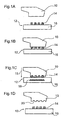
Figures 1A to 1D schematically represent successive phases of a first embodiment of the process of the invention; -
Figures 2A to 2D schematically represent successive phases of a second embodiment of the process of the invention; -
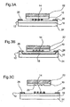
Figures 3A to 3C schematically represent successive phases of a third embodiment of the process of the invention; -
Figures 4A to 4C schematically represent successive phases of a fourth embodiment of the process of the invention; -
Figures 5A to 5E schematically represent successive phases in the production of a die for use in a process of the invention; and -
Figures 6A and 6B are micrographs of thermoplastic material showing the desired imprinting pattern after performance of the process of the invention. - A nano-impression lithographic process to form a pattern in relief on a mass of
polymeric material 10 having any desired three dimensional form (figure 1A ) to prepare adie 12 having asurface region 14 facing towards the body ofpolymeric material 10 and which reproduces in negative the pattern in relief to be impressed into thematerial 10. - The body of the
die 12 is of an electricallyconductive material 16 preferably having a resistivity of less than 1 Ω*m and more preferably less than 0.0001 Ω*m. For example it can be a semi-conductor, preferably Si or SiC, or a metal, preferably chosen from the group consisting of Ti, Ni, Cr, Cu, Ag, Au, W, Ir, Ta, Pd, Mo, V and their alloys. - The
polymeric material 10 can be of thermoplastic type and is for example chosen from the group consisting of polycarbonates, polymethylmethacrylates, polyethyl methacrylates, polyethylene terephthalates, polyolefins and their mixtures. The mass ofpolymeric material 10 is then (figure 1B ) brought into contact with and pressed against thedie 12. The contact under pressure can be obtained in a conventional manner by mechanical action, or by electrostatic, magnetic or electro-magnetic force and/or with acoustic shock waves. Contemporaneously with the contact phase anelectric current 16 is caused to pass (figure 1C ) through the body of thedie 12 where, by the Joule effect, it thus generates heat which is transmitted by conduction to thesurface region 14. The passage of the current 18 may for example be caused by the application of a potential difference or exposure to a variable electro-magnetic or magnetic field. Preferably, the direction of the main flow ofelectric current 18 is perpendicular to thedirection 19 of movement of the mass ofpolymeric material 10 with respect to the die 12. - The duration of the heating phase - intended as that in which the
polymeric material 10 is brought to a temperature greater than its glass transition temperature at which it behave as a viscous liquid and is subject to softening - is typically less than 25 seconds, preferably less than 50 milliseconds. In this phase the pattern on thezone 14 of the die is impressed into thepolymeric material 10. Then this latter is left to cool by diffusion and it is separated (figure 1D ) from thedie 12, leaving exposed the pattern inrelief 20 thus obtained. This separation is encouraged if at least a portion of the surface of the die 12 has been preliminarily coated with a release agent. - Figures from 2A to 2D illustrate the various phases of an alternative embodiment of the process of the invention, in which the same reference numerals as those previously utilised again distinguish the same or equivalent parts.
- In this case, the mass of
polymeric material 10 has a two-dimensional form and constitutes a sheet or thin film (for example of thickness - constant or variable - less than 2µm) deposited on asubstrate 22. - The body of the
die 12 has a layered structure and comprises afirst layer 16 of material having a resistivity less than 10 Ω*m and which supports thesurface region 14 which produces in negative form the pattern in relief to be impressed onto thepolymeric material 10, and asecond layer 24 of rigid material. Thesecond layer 24 can be of dielectric material, for example silicon dioxide, glass, quartz, sapphire or ceramic or semi-conductor, for example silicon, or metal, for example nickel or chrome. Further examples of material of thesecond layer 24 are silicon nitride, silicon carbide, semi-conductive and photoconductive mixtures. - In alternative embodiments of the invention, not illustrated, the
second layer 24 may also have a layered structure and be constituted by two or more different substrates. In this case at least one of these substrates is of material having low electrical and thermal conductivity. - The various phases of the lithographic process are substantially similar to those described with reference to
figures 1A - 1D , with the difference that in this case the pattern in relief is impressed onto a sheet or film rather than onto the surface of a three dimensional object. This latter can then be treated with an attack agent (for example by means of "reactive ion etching" or other technology based on the use of a plasma of reactive ions), so as to remove the polymeric material where it has been compressed and leave exposed theunderlying substrate 22. - Figures from 3A to 3C illustrate the various phases of an alternative embodiment of the process of the invention, in which the same reference numerals as those previously utilised in
figures 2A - 2D indicate equal or equivalent parts. - In this case, too, the body of the die 12 has a layered structure and includes a
surface layer 16 of a material having a resistivity less than 1 Ω*m, or preferably less than 0.0001 Ω*m and which supports thesurface region 14 which reproduces in negative form the pattern in relief to be impressed onto thepolymeric material 10, and a secondunderlying layer 24. - The layered structures of the body of the die 12 can for example be a system of the silicon on insulation type (SOI), which involves the presence of a
thin surface layer 16 of crystalline silicon, an intermediate layer of silicon oxide (not visible in drawings) and abase layer 24 of massive silicon. Thesurface layer 16 is massively doped so as to be made very conductive and to reproduce in negative form on itssurface region 14 the pattern in relief to be impressed onto thepolymeric material 10. This pattern can be formed in a conventional manner by means of lithographic techniques such as e-beam lithography and a process for subtractive attack known as "reactive ion etching" or "RIE". Thesurface layer 16 haselectrodes 26 associated therewith so as to allow the introduction of an electric current which remains confined within it. The intermediate layer of silicon oxide in fact limits the flow of the current to thethin surface layer 16 and creates a barrier against propagation of heat towards thebase layer 24. - Alternatively, the body of the die 12 may have a surface layer of strongly doped
silicon 16 and abase layer 24 of intrinsic silicon. Such a structure can be formed by means of an ion implantation technique which makes it possible accurately to control the doping profile and the electrical conductivity of the silicon. The shaping of thesurface profile 16 can be performed both before and after the ion implantation process. In this case, too, the presence ofelectrodes 26 on thesurface layer 16 permits the flow of current substantially to this latter because of the very much lower conductivity of theunderlying layer 24. - The various phases of the lithographic process are substantially similar to those described with reference to
figures 2A - 2D . However, the use of a base layer of silicon as theregion 16 of the die 12 in which dissipation of heat takes place offers the further advantage of being able to utilise the conventional methods of fabrication of the dies for NIL to shape itssurface 14 intended to impress thepolymeric material 10. Thissurface 14 can moreover be covered with release agents which promote its separation from the die 12 once the impression has been made. -
Figures 4A to 4C illustrate the various phases of an alternative embodiment of the process of the invention, in which the same reference numerals as those previously used indicate the same or equivalent parts. - In this case, too, the
die 12 has a layered structure and includes asurface layer 16 of material capable of heating upon exposure to electromagnetic radiation, preferably tomicrowaves 28, and abase layer 24 of material which is substantially transparent to electromagnetic radiation. Examples of material of thebase layer 24 are silicon oxide, glass, quartz, sapphire, ceramics, semiconductor materials, in particular silicon. Thebase layer 24 may, in turn, have a layered structure and may be formed by two or more sublayers. - The various phases of the lithographic process are substantially similar to those described with reference to
figures 2A - 2D with the difference that the generation of heat in theregion 16 is caused by its exposure to electromagnetic energy rather than by the passage of an electric current. This phenomenon is know as dielectric heating and is based on the principle of the rapid pre-polarisation of the molecules exposed to an electromagnetic field at high frequency. - There will now be described an exemplary embodiment of the process of the invention which, in the first place, envisages the use of a die provided with a heating element.
- For this purpose a layered structure (
figure 5A ) is prepared having, in succession, alayer 30 of Si of thickness of 500 µm, alayer 32 of SiO2 of thickness 5 µm, adouble layer 34 of Cu/Au ofthickness 20/10 nm and alayer 36 of photoresist having a thickness of 3 µm. This latter layer is subjected to optical lithography (figure 5B ) for removal of the residue of the photoresist by means of O2 plasma. Then an electrolytic deposition (electroplating) is effected with nickel 38 (figure 5C ) and the residual photoresist is stripped (figure 5D ). Finally, a contact shoe (figure 5E ) of thelayer 38 is formed with nickel having a thickness of 20 µm, which is welded with two external electric contacts not illustrated in the drawings. It is to be noted that the continuity of thenickel layer 38 is not interrupted and that it is apparently discontinuous in the drawing described above solely due to the fact that only a single section is illustrated therein. - In the die as formed the heating element is constituted by the
layer 38 the profile of which will be reproduced in negative on a polymeric material, in particular of thermoplastic type. - As already previously described, the process of the invention allows the polymeric material to be subject to nano-impression to be heated without raising the overall temperature of the sample containing this material, nor that of the die. To slow down the propagation of heat to the layers underlying the
layer 38 it is important that this latter be disposed above a material with low thermal conductivity, such as the silicon oxide of thelayer 32, which has been produced by a thermal growth process. On thelayer 32 there is then deposited by evaporation adouble layer 34 of chrome and gold, serving as a base for the subsequent electrolytic deposition phase (electroplating of nickel). Thelayer 36 of photoresist is then deposited on thelayer 34, for optical lithography. - The finished die covers a surface of 2x2 cm2 and this surface is completely heatable by means of the passage of current.
- The die was electrically connected to a pulsed supply system able to provide peaks of power greater than 1 MW.
- This die was utilised to subject to nano-impression a sample formed by a substrate of silicon of dimensions 1x1 cm2 covered by means of spin coating with a layer of 2 µm of thickness of polyethylmethacrylate (PEMA) which constitutes the thermoplastic material to be printed. Other polymers were also utilised such as polymethylmethacrylate (PMMA) and the commercial polymer Zeonex. The use of PEMA instead of PMMA was advantageous to reduce the printing temperatures.
- The nano-impression process was performed by bringing the surface of the die and the thermoplastic material into contact and pressing one against the other by means of a press observing the following process parameters:
- pressure: 8 MPa
- duration of current pulses provided by the generator: 500 µs
- voltage peak: 40 V
- current peak: 170 A
- repetition frequency: 50 Hz
- duration of the process: 20 sec (∼1000 pulses)
- Micrographs of the thermoplastic material having, after the above described process, the desired imprinting pattern are shown in
figures 6A and 6B . - Naturally, the principle of the invention remaining the same, the details of performance and the embodiments can be widely varied with respect to what has been described purely by way of non-limitative example, without by this departing from the ambit of the invention. In particular, it is possible to effect a pre-heating of the die and/or to bring it into contact with the mass of polymeric material with a pressure of pulsed type. It is, moreover, possible to arrange that the heating phase includes a plurality of short successive cycles in such a way that the impression of the pattern is the result of a series of successive indentations of the die. If necessary, it is further possible to effect a plurality of successive cycles of heating, contacting and separation, so as to print from time to time a certain pattern in relief on different portions of the mass of polymeric material. It is moreover possible locally to vary, in the limit even point by point, the quantity of thermal energy generated within the die, so as to adapt the characteristics of the process to specific requirements of use.
- It is also possible to form the heating region of the die in the form of an extended capacitor comprising a sequence of metal-dielectric-metal layers. The dissipation of energy can be produced by resistive effects connected to the charging-discharging of such extended capacitor by the application of an alternating current (particularly in the frequency range 1 MHz - 10 GHz) between the metal layers.
Claims (31)
- A lithographic process for forming a pattern (20) in relief on a mass (10) of polymeric material comprising the steps of:preparing the said mass (10) of polymeric material and a die (12) having a surface region (14) facing towards the said mass (10) of polymeric material and which reproduces in negative the said pattern in relief (20),heating the said die (12) and putting the said mass (10) of polymeric material into contact with the die (12) in any temporal sequence in such a way that the parts of the said mass (10) of the polymeric material in contact with the said surface zone (14) are subject to softening, andseparating the said die (12) from the mass (10) of polymeric material on the surface of which the said pattern in relief (20) has been formed,the said process being characterised by the fact that the heating of at least part of the die (12) is obtained by the generation of thermal energy upon dissipation of another form of energy in one region (16) of the said die (12), which is in the form of a layer which remains for less than 25 seconds at a temperature greater than or equal to the glass treatment temperature of the polymeric material (10).
- A process according to Claim 1, characterised in that the said mass (10) of polymeric material has a three-dimensional form.
- A process according to Claim 1, characterised in that the region (16) in which energy is dissipated with consequent generation of heat is at a smaller distance than 100 µm from the surface carrying the pattern in relief of the said die (12).
- A process according to Claim 1, characterised in that the said mass (10) of polymeric material has a two-dimensional form and is in the form of a sheet or thin film deposited on a substrate (22).
- A process according to any preceding claim, characterised in that the region (16) of the said die (12) in which thermal energy is generated remains for less than 50 milliseconds at a temperature greater than or equal to the glass transition temperature of the polymeric material (10).
- A process according to any preceding claim, characterised in that it includes a plurality of successive cycles of heating, contacting and separation.
- A process according to any preceding claim, characterised in that the heating phase includes a plurality of short successive cycles in such a way that the impression of the pattern is the result of a series of successive indentations of the die (12).
- A process according to any preceding claim, characterised in that the steps of heating the region (16) of the die (12) and contacting it with the mass (10) of polymeric material are synchronised.
- A process according to any preceding claim, characterised in that the said die (12) is put into contact under pressure with the mass (10) of polymeric material.
- A process according to Claim 9, characterised in that the said pressure is exerted in a pulsed manner.
- A process according to claim 9 or Claim 10, characterised that the said pressure is obtained mechanically, or with electrostatic, magnetic, electromagnetic forces and/or with acoustic shock waves.
- A process according to any preceding claim, characterised in that the said die (12) is pre-heated to a desired temperature.
- A process according to any preceding claim, characterised in that the quantity of thermal energy generated varies locally within the said region (16) of the die (12) .
- A process according to any preceding claim, characterised in that the said polymeric material (10) is of thermoplastic type.
- A process according to Claim 14, characterised in that the said polymeric material (10) is chosen from the group consisting of polycarbonates, polymethylmethacrylates, polyethylene terephthalates, polyethylmethacrylates, polybutylene terephthalates, polyolefins and their mixtures.
- A process according to any preceding claim, characterised in that at least one portion of the surface of the die (12) is clad with a release agent.
- A process according to any preceding claim, characterised in that , after the pattern (20) in relief has been formed on the surface of the mass (10) of polymeric material, a treatment is performed with an attack agent so as to remove the polymeric material (10) where it has been compressed.
- A process according to any preceding claim, characterised in that the surface region (14) of the die (12) which reproduces the pattern in relief in negative is aligned with pre-existing reference signs on the mass (10) of polymeric material or, if the said material (10) is a thin film, on the substrate (22) on which the said film is deposited.
- A process according to any preceding claim, characterised in that the said region (16) of the die (12) in which thermal energy is generated is of electrically conductive material.
- A process according to Claim 19, characterised in that the energy dissipated in heat is provided by an electric current (18) which flows in the said electrically conductive material.
- process according to Claim 20, characterised in that the direction of flow of the said electric current (18) is substantially perpendicular to the direction of relative movement of the mass (10) of polymeric material and the die (12).
- A process according to any preceding claim, characterised in that the said region (16) of the die (12) in which thermal energy is generated coincides with the said surface region (14) which reproduces the said pattern in relief in negative.
- A process according to Claim 1, characterised in that the said layer has a thickness less than 2 µm.
- A process according to Claim 1, characterised in that the said layer has a non-uniform thickness in such a way that it is possible locally to vary the quantity of thermal energy generated.
- A process according to any preceding claim from 19 to 24, characterised in that the said electrically conductive material is a metal, preferably chosen from the group consisting of Ti, Ni, Cr, Cu, Ag, Au, W, Ir, Ta, Pd, Mo, V and their alloys.
- A process according to any preceding claim from 19 to 24, characterised in that the said electrically conductive material is a semi-conductor, preferably silicon.
- A process according to any preceding claim from 1 to 24, characterised in that the said layer of electrically conductive material is obtained by doping a surface layer (16) of an intrinsically semiconductive or initially lightly-doped substrate, in such a way as to increase its conductivity with respect to the underlying portion (24) of the substrate.
- A process according to Claim 27, characterised in that the said layer (16) to be doped is the outermost layer of silicon of a silicon-on-insulator (SOI) structure.
- A process according to Claim 27, characterised in that the doping operation is performed by ion implantation.
- A process according to any preceding claim from 20 to 29, characterised in that the said electric current (18) is induced by applying a potential difference between at least two electrodes (26) connected to the said electrically conductive material.
- A process according to any preceding claim from 20 to 29, characterised in that the said electric current (18) is induced by a variable magnetic field.
Applications Claiming Priority (2)
| Application Number | Priority Date | Filing Date | Title |
|---|---|---|---|
| IT000473A ITTO20030473A1 (en) | 2003-06-23 | 2003-06-23 | LITOGRAPHIC NANOIMPRESSION PROCEDURE WHICH PROVIDES THE USE OF A MOLD PRESENTING A REGION SUITABLE FOR |
| PCT/IB2004/002120 WO2004114017A1 (en) | 2003-06-23 | 2004-06-22 | A nano impression lithographic process which involves the use of a die having a region able to generate heat |
Publications (2)
| Publication Number | Publication Date |
|---|---|
| EP1639411A1 EP1639411A1 (en) | 2006-03-29 |
| EP1639411B1 true EP1639411B1 (en) | 2010-08-04 |
Family
ID=33524062
Family Applications (1)
| Application Number | Title | Priority Date | Filing Date |
|---|---|---|---|
| EP04743806A Expired - Lifetime EP1639411B1 (en) | 2003-06-23 | 2004-06-22 | A nano impression lithographic process which involves the use of a die having a region able to generate heat |
Country Status (7)
| Country | Link |
|---|---|
| US (1) | US8409488B2 (en) |
| EP (1) | EP1639411B1 (en) |
| AT (1) | ATE476685T1 (en) |
| DE (1) | DE602004028475D1 (en) |
| DK (1) | DK1639411T3 (en) |
| IT (1) | ITTO20030473A1 (en) |
| WO (1) | WO2004114017A1 (en) |
Cited By (1)
| Publication number | Priority date | Publication date | Assignee | Title |
|---|---|---|---|---|
| EP3125042A2 (en) | 2015-07-31 | 2017-02-01 | Giesecke & Devrient GmbH | Nanoimprint mold |
Families Citing this family (10)
| Publication number | Priority date | Publication date | Assignee | Title |
|---|---|---|---|---|
| TWI243796B (en) * | 2004-06-08 | 2005-11-21 | Ind Tech Res Inst | Device of nano-structure imprint for pattern transfer and method of the same |
| FR2876193B1 (en) * | 2004-10-04 | 2007-01-26 | Commissariat Energie Atomique | NANOIMPRIME DEVICE COMPRISING METALLIC PATTERNS AND METHOD FOR NANOIMPRESSING METAL PATTERNS |
| JP4554330B2 (en) * | 2004-10-21 | 2010-09-29 | 株式会社リコー | High durability heat insulating stamper structure |
| FR2950043B1 (en) | 2009-09-17 | 2011-10-14 | Commissariat Energie Atomique | MOLD FOR THERMAL NANOIMPRESSION LITHOGRAPHY, PROCESS FOR PREPARING THE SAME, AND THERMAL NANOIMPRESSION METHOD FOR CARRYING OUT THE SAME. |
| CN101829772B (en) * | 2010-05-26 | 2011-11-02 | 浙江大学 | Thermoplasticity shaping and processing method of metal glass micro construction member |
| FR2964338B1 (en) * | 2010-09-07 | 2012-10-05 | Commissariat Energie Atomique | MOLD FOR THERMAL NANO-PRINTING LITHOGRAPHY, PROCESS FOR PREPARING THE SAME, AND THERMAL NANO-PRINTING METHOD USING THE SAME |
| US9498918B2 (en) | 2012-09-18 | 2016-11-22 | Ev Group E. Thallner Gmbh | Method and device for embossing |
| US20160193824A1 (en) * | 2013-08-12 | 2016-07-07 | Tufts University | Micro forming devices and systems and uses thereof |
| TWI628062B (en) * | 2016-03-17 | 2018-07-01 | 欣興電子股份有限公司 | Method for manufacturing circuit board and piezochromic stamp |
| CN116722368A (en) * | 2023-06-25 | 2023-09-08 | 北京信息科技大学 | A kind of metasurface structure and preparation method thereof |
Family Cites Families (11)
| Publication number | Priority date | Publication date | Assignee | Title |
|---|---|---|---|---|
| US1864666A (en) | 1930-04-04 | 1932-06-28 | John F Osborne | Electric mold |
| US2210583A (en) | 1939-03-04 | 1940-08-06 | Owens Illinois Glass Co | Mold |
| US3387333A (en) | 1965-01-27 | 1968-06-11 | Lockheed Aircraft Corp | Electrically heated mold |
| DE3677005D1 (en) * | 1986-05-06 | 1991-02-21 | Ibm Deutschland | MASK FOR ION, ELECTRON OR X-RAY RAY LITHOGRAPHY AND METHOD FOR THE PRODUCTION THEREOF. |
| US5064597A (en) * | 1988-03-30 | 1991-11-12 | General Electric Company | Method of compression molding on hot surfaces |
| JPH0580530A (en) * | 1991-09-24 | 1993-04-02 | Hitachi Ltd | Production of thin film pattern |
| US5261806A (en) * | 1992-02-26 | 1993-11-16 | Pleasant Ronald E | Electrically heated mold insert |
| US5772905A (en) | 1995-11-15 | 1998-06-30 | Regents Of The University Of Minnesota | Nanoimprint lithography |
| US6517995B1 (en) | 1999-09-14 | 2003-02-11 | Massachusetts Institute Of Technology | Fabrication of finely featured devices by liquid embossing |
| US6755984B2 (en) * | 2002-10-24 | 2004-06-29 | Hewlett-Packard Development Company, L.P. | Micro-casted silicon carbide nano-imprinting stamp |
| US7291004B2 (en) | 2002-12-31 | 2007-11-06 | Industry-Academic Cooperation Foundation, Yonsei University | Molding system having a micro heating element for molding a micro pattern structure |
-
2003
- 2003-06-23 IT IT000473A patent/ITTO20030473A1/en unknown
-
2004
- 2004-06-22 DK DK04743806.4T patent/DK1639411T3/en active
- 2004-06-22 US US10/562,014 patent/US8409488B2/en not_active Expired - Fee Related
- 2004-06-22 AT AT04743806T patent/ATE476685T1/en active
- 2004-06-22 DE DE602004028475T patent/DE602004028475D1/en not_active Expired - Lifetime
- 2004-06-22 WO PCT/IB2004/002120 patent/WO2004114017A1/en not_active Ceased
- 2004-06-22 EP EP04743806A patent/EP1639411B1/en not_active Expired - Lifetime
Cited By (2)
| Publication number | Priority date | Publication date | Assignee | Title |
|---|---|---|---|---|
| EP3125042A2 (en) | 2015-07-31 | 2017-02-01 | Giesecke & Devrient GmbH | Nanoimprint mold |
| DE102015009982A1 (en) | 2015-07-31 | 2017-02-02 | Giesecke & Devrient Gmbh | Embossing stamp for the nanoimprint lithography |
Also Published As
| Publication number | Publication date |
|---|---|
| WO2004114017A1 (en) | 2004-12-29 |
| DK1639411T3 (en) | 2010-11-22 |
| US20070063390A1 (en) | 2007-03-22 |
| DE602004028475D1 (en) | 2010-09-16 |
| EP1639411A1 (en) | 2006-03-29 |
| ATE476685T1 (en) | 2010-08-15 |
| US8409488B2 (en) | 2013-04-02 |
| ITTO20030473A1 (en) | 2004-12-24 |
Similar Documents
| Publication | Publication Date | Title |
|---|---|---|
| EP1509379B1 (en) | Methods and apparatus of field-induced pressure imprint lithography | |
| TW512129B (en) | Method for forming microelectronic spring structures on a substrate | |
| US6964793B2 (en) | Method for fabricating nanoscale patterns in light curable compositions using an electric field | |
| US8409488B2 (en) | Nano impression lithographic process which involves the use of a die having a region able to generate heat | |
| TWI358608B (en) | Method to reduce adhesion between a conformable re | |
| DE19956654B4 (en) | Process for structuring surfaces of micromechanical and / or microoptical components and / or functional elements made of vitreous materials | |
| US20080106003A1 (en) | Methods and apparatus of pressure imprint lithography | |
| EP1290497B1 (en) | Method for the production of a template and the template thus produced | |
| US5772905A (en) | Nanoimprint lithography | |
| Youn et al. | Fabrication of micro-mold for glass embossing using focused ion beam, femto-second laser, eximer laser and dicing techniques | |
| CN101837950A (en) | Device and method for assembling nanostructure directly by using two-block copolymer | |
| CN110891895B (en) | Methods for micro- and nanofabrication by selective template removal | |
| WO2009078881A1 (en) | Imprint lithography apparatus and method | |
| KR100601263B1 (en) | Micro pattern formation method using rapid heating nano molding | |
| Mekaru | Formation of metal nanostructures by high-temperature imprinting | |
| JP4083725B2 (en) | Thin film transistor manufacturing method and manufacturing apparatus thereof | |
| US7052926B2 (en) | Fabrication of movable micromechanical components employing low-cost, high-resolution replication technology method | |
| TWI253434B (en) | Applying imprinting material to substrates employing electromagnetic fields | |
| KR100975785B1 (en) | Laser Assisted Direct Imprint Lithography | |
| JP2024509943A (en) | Method for facilitating mold release during pattern transfer | |
| KR100927481B1 (en) | Method of manufacturing micro-nano metal structures | |
| KR100492851B1 (en) | Method for fabricating micro pattern on surface by using buckling phenomenon | |
| JP2600097B2 (en) | Parts manufacturing method | |
| JPH09175835A (en) | Surface processing method | |
| Lee et al. | Contact printing of metallic pattern and its applications on fabricating high-frequency surface acoustic wave (SAW) devices |
Legal Events
| Date | Code | Title | Description |
|---|---|---|---|
| PUAI | Public reference made under article 153(3) epc to a published international application that has entered the european phase |
Free format text: ORIGINAL CODE: 0009012 |
|
| 17P | Request for examination filed |
Effective date: 20060119 |
|
| AK | Designated contracting states |
Kind code of ref document: A1 Designated state(s): AT BE BG CH CY CZ DE DK EE ES FI FR GB GR HU IE IT LI LU MC NL PL PT RO SE SI SK TR |
|
| DAX | Request for extension of the european patent (deleted) | ||
| 17Q | First examination report despatched |
Effective date: 20080123 |
|
| GRAP | Despatch of communication of intention to grant a patent |
Free format text: ORIGINAL CODE: EPIDOSNIGR1 |
|
| GRAS | Grant fee paid |
Free format text: ORIGINAL CODE: EPIDOSNIGR3 |
|
| GRAA | (expected) grant |
Free format text: ORIGINAL CODE: 0009210 |
|
| RAP1 | Party data changed (applicant data changed or rights of an application transferred) |
Owner name: CONSIGLIO NAZIONALE DELLE RICERCHE |
|
| AK | Designated contracting states |
Kind code of ref document: B1 Designated state(s): AT BE BG CH CY CZ DE DK EE ES FI FR GB GR HU IE IT LI LU MC NL PL PT RO SE SI SK TR |
|
| REG | Reference to a national code |
Ref country code: GB Ref legal event code: FG4D |
|
| REG | Reference to a national code |
Ref country code: CH Ref legal event code: EP |
|
| REG | Reference to a national code |
Ref country code: IE Ref legal event code: FG4D |
|
| REF | Corresponds to: |
Ref document number: 602004028475 Country of ref document: DE Date of ref document: 20100916 Kind code of ref document: P |
|
| REG | Reference to a national code |
Ref country code: SE Ref legal event code: TRGR |
|
| REG | Reference to a national code |
Ref country code: CH Ref legal event code: NV Representative=s name: JACOBACCI & PARTNERS S.P.A. |
|
| REG | Reference to a national code |
Ref country code: NL Ref legal event code: T3 |
|
| REG | Reference to a national code |
Ref country code: DK Ref legal event code: T3 |
|
| PG25 | Lapsed in a contracting state [announced via postgrant information from national office to epo] |
Ref country code: BG Free format text: LAPSE BECAUSE OF FAILURE TO SUBMIT A TRANSLATION OF THE DESCRIPTION OR TO PAY THE FEE WITHIN THE PRESCRIBED TIME-LIMIT Effective date: 20101104 Ref country code: CY Free format text: LAPSE BECAUSE OF FAILURE TO SUBMIT A TRANSLATION OF THE DESCRIPTION OR TO PAY THE FEE WITHIN THE PRESCRIBED TIME-LIMIT Effective date: 20100804 Ref country code: PT Free format text: LAPSE BECAUSE OF FAILURE TO SUBMIT A TRANSLATION OF THE DESCRIPTION OR TO PAY THE FEE WITHIN THE PRESCRIBED TIME-LIMIT Effective date: 20101206 Ref country code: SI Free format text: LAPSE BECAUSE OF FAILURE TO SUBMIT A TRANSLATION OF THE DESCRIPTION OR TO PAY THE FEE WITHIN THE PRESCRIBED TIME-LIMIT Effective date: 20100804 Ref country code: PL Free format text: LAPSE BECAUSE OF FAILURE TO SUBMIT A TRANSLATION OF THE DESCRIPTION OR TO PAY THE FEE WITHIN THE PRESCRIBED TIME-LIMIT Effective date: 20100804 |
|
| PG25 | Lapsed in a contracting state [announced via postgrant information from national office to epo] |
Ref country code: BE Free format text: LAPSE BECAUSE OF FAILURE TO SUBMIT A TRANSLATION OF THE DESCRIPTION OR TO PAY THE FEE WITHIN THE PRESCRIBED TIME-LIMIT Effective date: 20100804 Ref country code: GR Free format text: LAPSE BECAUSE OF FAILURE TO SUBMIT A TRANSLATION OF THE DESCRIPTION OR TO PAY THE FEE WITHIN THE PRESCRIBED TIME-LIMIT Effective date: 20101105 |
|
| PG25 | Lapsed in a contracting state [announced via postgrant information from national office to epo] |
Ref country code: SK Free format text: LAPSE BECAUSE OF FAILURE TO SUBMIT A TRANSLATION OF THE DESCRIPTION OR TO PAY THE FEE WITHIN THE PRESCRIBED TIME-LIMIT Effective date: 20100804 Ref country code: RO Free format text: LAPSE BECAUSE OF FAILURE TO SUBMIT A TRANSLATION OF THE DESCRIPTION OR TO PAY THE FEE WITHIN THE PRESCRIBED TIME-LIMIT Effective date: 20100804 Ref country code: EE Free format text: LAPSE BECAUSE OF FAILURE TO SUBMIT A TRANSLATION OF THE DESCRIPTION OR TO PAY THE FEE WITHIN THE PRESCRIBED TIME-LIMIT Effective date: 20100804 Ref country code: CZ Free format text: LAPSE BECAUSE OF FAILURE TO SUBMIT A TRANSLATION OF THE DESCRIPTION OR TO PAY THE FEE WITHIN THE PRESCRIBED TIME-LIMIT Effective date: 20100804 |
|
| PLBE | No opposition filed within time limit |
Free format text: ORIGINAL CODE: 0009261 |
|
| STAA | Information on the status of an ep patent application or granted ep patent |
Free format text: STATUS: NO OPPOSITION FILED WITHIN TIME LIMIT |
|
| PG25 | Lapsed in a contracting state [announced via postgrant information from national office to epo] |
Ref country code: ES Free format text: LAPSE BECAUSE OF FAILURE TO SUBMIT A TRANSLATION OF THE DESCRIPTION OR TO PAY THE FEE WITHIN THE PRESCRIBED TIME-LIMIT Effective date: 20101115 |
|
| 26N | No opposition filed |
Effective date: 20110506 |
|
| REG | Reference to a national code |
Ref country code: DE Ref legal event code: R097 Ref document number: 602004028475 Country of ref document: DE Effective date: 20110506 |
|
| PG25 | Lapsed in a contracting state [announced via postgrant information from national office to epo] |
Ref country code: MC Free format text: LAPSE BECAUSE OF NON-PAYMENT OF DUE FEES Effective date: 20110630 |
|
| PG25 | Lapsed in a contracting state [announced via postgrant information from national office to epo] |
Ref country code: LU Free format text: LAPSE BECAUSE OF NON-PAYMENT OF DUE FEES Effective date: 20110622 |
|
| PG25 | Lapsed in a contracting state [announced via postgrant information from national office to epo] |
Ref country code: TR Free format text: LAPSE BECAUSE OF FAILURE TO SUBMIT A TRANSLATION OF THE DESCRIPTION OR TO PAY THE FEE WITHIN THE PRESCRIBED TIME-LIMIT Effective date: 20100804 |
|
| PG25 | Lapsed in a contracting state [announced via postgrant information from national office to epo] |
Ref country code: HU Free format text: LAPSE BECAUSE OF FAILURE TO SUBMIT A TRANSLATION OF THE DESCRIPTION OR TO PAY THE FEE WITHIN THE PRESCRIBED TIME-LIMIT Effective date: 20100804 |
|
| PGFP | Annual fee paid to national office [announced via postgrant information from national office to epo] |
Ref country code: IE Payment date: 20140625 Year of fee payment: 11 |
|
| REG | Reference to a national code |
Ref country code: CH Ref legal event code: PCAR Free format text: NEW ADDRESS: VIA LUGANETTO 3, 6962 LUGANO (CH) |
|
| REG | Reference to a national code |
Ref country code: IE Ref legal event code: MM4A |
|
| PG25 | Lapsed in a contracting state [announced via postgrant information from national office to epo] |
Ref country code: IE Free format text: LAPSE BECAUSE OF NON-PAYMENT OF DUE FEES Effective date: 20150622 |
|
| REG | Reference to a national code |
Ref country code: FR Ref legal event code: PLFP Year of fee payment: 13 |
|
| PGFP | Annual fee paid to national office [announced via postgrant information from national office to epo] |
Ref country code: FI Payment date: 20160616 Year of fee payment: 13 |
|
| REG | Reference to a national code |
Ref country code: FR Ref legal event code: PLFP Year of fee payment: 14 |
|
| PG25 | Lapsed in a contracting state [announced via postgrant information from national office to epo] |
Ref country code: FI Free format text: LAPSE BECAUSE OF NON-PAYMENT OF DUE FEES Effective date: 20170622 |
|
| REG | Reference to a national code |
Ref country code: FR Ref legal event code: PLFP Year of fee payment: 15 |
|
| PGFP | Annual fee paid to national office [announced via postgrant information from national office to epo] |
Ref country code: SE Payment date: 20220623 Year of fee payment: 19 Ref country code: NL Payment date: 20220620 Year of fee payment: 19 Ref country code: GB Payment date: 20220622 Year of fee payment: 19 Ref country code: DK Payment date: 20220622 Year of fee payment: 19 |
|
| PGFP | Annual fee paid to national office [announced via postgrant information from national office to epo] |
Ref country code: AT Payment date: 20220621 Year of fee payment: 19 |
|
| PGFP | Annual fee paid to national office [announced via postgrant information from national office to epo] |
Ref country code: FR Payment date: 20220627 Year of fee payment: 19 |
|
| PGFP | Annual fee paid to national office [announced via postgrant information from national office to epo] |
Ref country code: DE Payment date: 20220620 Year of fee payment: 19 |
|
| PGFP | Annual fee paid to national office [announced via postgrant information from national office to epo] |
Ref country code: CH Payment date: 20220701 Year of fee payment: 19 |
|
| PGFP | Annual fee paid to national office [announced via postgrant information from national office to epo] |
Ref country code: IT Payment date: 20230525 Year of fee payment: 20 |
|
| REG | Reference to a national code |
Ref country code: DE Ref legal event code: R119 Ref document number: 602004028475 Country of ref document: DE |
|
| REG | Reference to a national code |
Ref country code: DK Ref legal event code: EBP Effective date: 20230630 |
|
| REG | Reference to a national code |
Ref country code: SE Ref legal event code: EUG |
|
| REG | Reference to a national code |
Ref country code: CH Ref legal event code: PL |
|
| REG | Reference to a national code |
Ref country code: NL Ref legal event code: MM Effective date: 20230701 |
|
| REG | Reference to a national code |
Ref country code: AT Ref legal event code: MM01 Ref document number: 476685 Country of ref document: AT Kind code of ref document: T Effective date: 20230622 |
|
| GBPC | Gb: european patent ceased through non-payment of renewal fee |
Effective date: 20230622 |
|
| PG25 | Lapsed in a contracting state [announced via postgrant information from national office to epo] |
Ref country code: NL Free format text: LAPSE BECAUSE OF NON-PAYMENT OF DUE FEES Effective date: 20230701 |
|
| PG25 | Lapsed in a contracting state [announced via postgrant information from national office to epo] |
Ref country code: AT Free format text: LAPSE BECAUSE OF NON-PAYMENT OF DUE FEES Effective date: 20230622 |
|
| PG25 | Lapsed in a contracting state [announced via postgrant information from national office to epo] |
Ref country code: DE Free format text: LAPSE BECAUSE OF NON-PAYMENT OF DUE FEES Effective date: 20240103 Ref country code: AT Free format text: LAPSE BECAUSE OF NON-PAYMENT OF DUE FEES Effective date: 20230622 Ref country code: CH Free format text: LAPSE BECAUSE OF NON-PAYMENT OF DUE FEES Effective date: 20230630 Ref country code: GB Free format text: LAPSE BECAUSE OF NON-PAYMENT OF DUE FEES Effective date: 20230622 |
|
| PG25 | Lapsed in a contracting state [announced via postgrant information from national office to epo] |
Ref country code: SE Free format text: LAPSE BECAUSE OF NON-PAYMENT OF DUE FEES Effective date: 20230623 Ref country code: FR Free format text: LAPSE BECAUSE OF NON-PAYMENT OF DUE FEES Effective date: 20230630 |
|
| PG25 | Lapsed in a contracting state [announced via postgrant information from national office to epo] |
Ref country code: DK Free format text: LAPSE BECAUSE OF NON-PAYMENT OF DUE FEES Effective date: 20230630 |
|
| PG25 | Lapsed in a contracting state [announced via postgrant information from national office to epo] |
Ref country code: DK Free format text: LAPSE BECAUSE OF NON-PAYMENT OF DUE FEES Effective date: 20230630 |