EP1638372A1 - Charge-transporting varnish - Google Patents
Charge-transporting varnish Download PDFInfo
- Publication number
- EP1638372A1 EP1638372A1 EP04733958A EP04733958A EP1638372A1 EP 1638372 A1 EP1638372 A1 EP 1638372A1 EP 04733958 A EP04733958 A EP 04733958A EP 04733958 A EP04733958 A EP 04733958A EP 1638372 A1 EP1638372 A1 EP 1638372A1
- Authority
- EP
- European Patent Office
- Prior art keywords
- group
- charge
- transporting
- varnish
- transporting varnish
- Prior art date
- Legal status (The legal status is an assumption and is not a legal conclusion. Google has not performed a legal analysis and makes no representation as to the accuracy of the status listed.)
- Granted
Links
Classifications
-
- C—CHEMISTRY; METALLURGY
- C08—ORGANIC MACROMOLECULAR COMPOUNDS; THEIR PREPARATION OR CHEMICAL WORKING-UP; COMPOSITIONS BASED THEREON
- C08G—MACROMOLECULAR COMPOUNDS OBTAINED OTHERWISE THAN BY REACTIONS ONLY INVOLVING UNSATURATED CARBON-TO-CARBON BONDS
- C08G73/00—Macromolecular compounds obtained by reactions forming a linkage containing nitrogen with or without oxygen or carbon in the main chain of the macromolecule, not provided for in groups C08G12/00 - C08G71/00
- C08G73/02—Polyamines
- C08G73/026—Wholly aromatic polyamines
- C08G73/0266—Polyanilines or derivatives thereof
-
- C—CHEMISTRY; METALLURGY
- C09—DYES; PAINTS; POLISHES; NATURAL RESINS; ADHESIVES; COMPOSITIONS NOT OTHERWISE PROVIDED FOR; APPLICATIONS OF MATERIALS NOT OTHERWISE PROVIDED FOR
- C09K—MATERIALS FOR MISCELLANEOUS APPLICATIONS, NOT PROVIDED FOR ELSEWHERE
- C09K11/00—Luminescent materials, e.g. electroluminescent or chemiluminescent
- C09K11/06—Luminescent materials, e.g. electroluminescent or chemiluminescent containing organic luminescent materials
-
- H—ELECTRICITY
- H01—ELECTRIC ELEMENTS
- H01B—CABLES; CONDUCTORS; INSULATORS; SELECTION OF MATERIALS FOR THEIR CONDUCTIVE, INSULATING OR DIELECTRIC PROPERTIES
- H01B1/00—Conductors or conductive bodies characterised by the conductive materials; Selection of materials as conductors
- H01B1/06—Conductors or conductive bodies characterised by the conductive materials; Selection of materials as conductors mainly consisting of other non-metallic substances
- H01B1/12—Conductors or conductive bodies characterised by the conductive materials; Selection of materials as conductors mainly consisting of other non-metallic substances organic substances
- H01B1/124—Intrinsically conductive polymers
- H01B1/128—Intrinsically conductive polymers comprising six-membered aromatic rings in the main chain, e.g. polyanilines, polyphenylenes
-
- H—ELECTRICITY
- H05—ELECTRIC TECHNIQUES NOT OTHERWISE PROVIDED FOR
- H05B—ELECTRIC HEATING; ELECTRIC LIGHT SOURCES NOT OTHERWISE PROVIDED FOR; CIRCUIT ARRANGEMENTS FOR ELECTRIC LIGHT SOURCES, IN GENERAL
- H05B33/00—Electroluminescent light sources
- H05B33/12—Light sources with substantially two-dimensional [2D] radiating surfaces
- H05B33/22—Light sources with substantially two-dimensional [2D] radiating surfaces characterised by the chemical or physical composition or the arrangement of auxiliary dielectric or reflective layers
-
- H—ELECTRICITY
- H10—SEMICONDUCTOR DEVICES; ELECTRIC SOLID-STATE DEVICES NOT OTHERWISE PROVIDED FOR
- H10K—ORGANIC ELECTRIC SOLID-STATE DEVICES
- H10K50/00—Organic light-emitting devices
- H10K50/10—OLEDs or polymer light-emitting diodes [PLED]
- H10K50/14—Carrier transporting layers
-
- H—ELECTRICITY
- H10—SEMICONDUCTOR DEVICES; ELECTRIC SOLID-STATE DEVICES NOT OTHERWISE PROVIDED FOR
- H10K—ORGANIC ELECTRIC SOLID-STATE DEVICES
- H10K50/00—Organic light-emitting devices
- H10K50/10—OLEDs or polymer light-emitting diodes [PLED]
- H10K50/17—Carrier injection layers
-
- H—ELECTRICITY
- H10—SEMICONDUCTOR DEVICES; ELECTRIC SOLID-STATE DEVICES NOT OTHERWISE PROVIDED FOR
- H10K—ORGANIC ELECTRIC SOLID-STATE DEVICES
- H10K85/00—Organic materials used in the body or electrodes of devices covered by this subclass
- H10K85/10—Organic polymers or oligomers
- H10K85/111—Organic polymers or oligomers comprising aromatic, heteroaromatic, or aryl chains, e.g. polyaniline, polyphenylene or polyphenylene vinylene
Definitions
- This invention relates to a charge-transporting varnish and, more particularly, to a charge-transporting varnish capable of forming, for example, a charge transporting thin film which is able to improve electric characteristics and life characteristic while preventing concentration phenomena of electric current and charge.
- This charge-transporting varnish is applicable as an organic electroluminescent (hereinafter referred to as EL) element, a capacitor element, an antistatic film and the like.
- Organic EL elements particularly, low molecular weight organic EL (hereinafter referred to as OLED), have been isolated function thereof by Eastman Kodak based on ultrathinning and multilayering of organic layers and are thus remarkably improved in characteristics such as drastic lowering of drive voltage (Applied Physics Letters, U.S.A., 1987, Vol. 51, pp. 913-915).
- OLED organic EL
- Cambridge University found an EL element using a polymeric fluorescent material (hereinafter referred to as PLED) (Nature, England, 1990, Vol. 347, pp. 539-541), which has now been improved in characteristics to such a level as to compare with conventional OLED elements.
- CuPC that has been ordinarily used as a hole injection material in OLED element has the drawback that it has drastic irregularities and thus, brings about a great characteristic lowering upon mixing in other organic layers in small amount.
- Polyaniline-type materials and polythiophene-type materials currently employed for PLED element involve problems in that they contain, as a solvent, water having capability of promoting element deterioration, limitation is placed on the choice of solvent, limitation is also placed on the manner of coating ensuring uniform film formation because of coagulation of material and low solubility, and a difficulty is involved in control of viscosity.
- An object of the invention is to provide a charge transporting varnish capable of achieving excellent conduction characteristics and obtained through firing within a short time in a system using an oligoaniline compound and a charge accepting dopant material.
- the present invention provides the following inventions [1] to [8].
- the charge transporting varnish of the invention differs from a conventionally employed charge transporting varnish in the form of an aqueous solution, and can be used only by use of an organic solvent.
- a charge transporting thin film of the invention on an electrode surface can prevent electric short-circuiting.
- the use of the charge transporting thin film as a charge injection layer of an organic EL element permits injection barrier to lower owing to the relaxation of ionization potentials of an electrode and an organic layer.
- application of conjugated oligomer groups to an organic EL element is enabled. From the foregoing, lowering of luminescence initiating voltage of an organic EL element, improvement of a current efficiency and prolonged life can be achieved.
- the charge transporting varnish of the invention is good with respect to thin film formation process and is useful for application to a capacitor electrode protection film and also to an antistatic film.
- the charge transporting varnish of the invention is one which contains a charge transporting material serving as a principal component for charge transporting mechanism and a solvent, or which contains a charge transporting material, a charge accepting dopant material for improving charge transportability and a solvent.
- the charge transporting material (and the charge accepting dopant material) are completely dissolved or homogeneously dispersed in the solvent.
- the transportability used herein has the same meaning as conductivity and means any one of hole transportability, electron transportability, and transportability of both hole and electron.
- the charge transporting varnish of the invention may exhibit charge transportability in itself, or may exhibit charge transportability after conversion to a solid film obtained by use of the varnish.
- the charge transporting material used in the present invention is an oligoaniline compound represented by the formula (1).
- R 1 represents a hydrogen atom, an unsubstituted or substituted monovalent hydrocarbon group, an organooxy group, or an acyl group
- R 2 and R 3 independently represent a hydrogen atom, an unsubstituted or substituted monovalent hydrocarbon group, or an acyl group
- R 4 to R 7 independently represent a hydrogen atom, a hydroxyl group, an unsubstituted or substituted monovalent hydrocarbon group, an organooxy group, an acyl group, or a sulfonic acid group
- m and n are independently an integer of 1 or over provided that m+2n ⁇ 20, and a quinoid moiety tautomerically exists at an arbitrary position of the structural formula.
- the substituent R 1 of the oligoaniline compound used in the invention is hydrogen, an unsubstituted or substituted monovalent hydrocarbon group, an organooxy group, or an acyl group, and R 2 and R 3 independently represent a hydrogen atom, an unsubstituted or substituted monovalent hydrocarbon group, or an acyl group.
- the monovalent hydrocarbon group and the organooxy group should preferably have 1 to 20 carbon atoms, and the acyl group should preferably have 2 to 20 carbon atoms.
- the monovalent hydrocarbon group includes, for example, an alkyl group such as a methyl group, an ethyl group, a propyl group, a butyl group, a t-butyl group, a hexyl group, an octyl group, an decyl group or the like, a cycloalkyl group such as a cyclopentyl group, a cyclohexyl group or the like, a bicycloalkyl group such as a bicyclohexyl group or the like, an alkenyl group such as a vinyl group, a 1-propenyl group, a 2-propenyl group, an isopropenyl group, a 1-methyl-2-propenyl group, a 1, 2 or 3-butenyl group, a
- an organooxy group includes an alkoxy group, an alkenyloxy group, an aryloxy group or the like.
- alkyl group, alkenyl group and aryl group mention is made of such groups as exemplified above.
- the acyl group includes one having 2 to 10 carbon atoms such as, for example, an acetyl group, a propionyl group, a butyryl group, an isobutyryl group, a valeryl group, an isovaleryl group, a benzyl group or the like.
- R 1 and R 2 include a hydrogen atom, an alkyl group having 1 to 20 carbon atoms, preferably 1 to 4 carbon atoms, a phenyl group, a cyclohexyl group, a cyclopentyl group, a biphenyl group, a bicyclohexyl group or a phenylcyclohexyl group (provided these phenyl, cyclohexyl, cyclopentyl, biphenyl, bicyclohexyl and phenylcyclohexyl groups may have a substituent such as an alkyl group or an alkoxy group having 1 to 4 carbon atoms.), or an acyl group having 2 to 4 carbon atoms.
- R 3 a hydrogen atom, an alkyl group having 1 to 4 carbon atoms, or a phenyl group which may have an alkoxy group as a substituent is preferred.
- R 1 is a hydrogen atom and R 3 is a phenyl group, i.e., the oligoaniline compound of the formula (1) is blocked with a phenyl group at both ends thereof, is preferred.
- the substituents R 4 to R 7 independently represent a hydrogen atom, a hydroxyl group, an unsubstituted or substituted monovalent hydrocarbon group, an organooxy group, an acyl group, and a sulfonic acid group.
- the unsubstituted or substituted monovalent hydrocarbon group and organooxy group should preferably have 2 to 20 carbon atoms, respectively, and the acyl group should preferably have 2 to 20 carbon atoms, and mention may be made of those groups as indicated with respect to R 1 .
- the substituents R 4 to R 7 preferably include a hydrogen atom, an alkyl group, an alkoxy group, an alkoxyalkyl group, an alkenyl group, an acyl group, a sulfonic acid group, and a hydroxyl group, or a phenyl group, a cyclohexyl group, a cyclopentyl group, a biphenyl group, a bicyclohexyl group or a phenylcyclohexyl group that may have a substituent of an alkyl group or alkoxy group each having 1 to 4 carbon atoms.
- R 4 to R 7 represents a hydrogen atom, an alkyl group having 1 to 20 carbon atoms, an alkoxy group having 1 to 20 carbon atoms, an alkoxyalkyl group wherein the alkoxy group has 1 to 20 carbon atoms and the alkyl group has 1 to 20 carbon atoms, an alkenyl group having 2 to 4 carbon atoms, an acyl group having 2 to 4 carbon atoms, a benzoyl group, a sulfonic acid group, a hydroxyl group, or a phenyl group, a cyclohexyl group, a cyclopentyl group, a biphenyl group, a bicyclohexyl group or a phenylcyclohexyl group that may have a substituent (wherein the substituent includes an alkyl group having 1 to 4 carbon atoms or an alkoxy group having 1 to 4 carbon atoms), respectively.
- a hydrogen atom an alkyl group having 1 to 4 carbon atoms, an alkoxy group having 1 to 4 carbon atoms, an alkoxyalkyl group wherein the alkoxy group has 1 to 4 carbon atoms and the alkyl group has 1 to 4 carbon atom, a vinyl group, a 2-propenyl group, an acetyl group, a benzoyl group, a sulfonic acid group, a hydroxyl group, or a phenyl group, a cyclohexyl group, a biphenyl group, a bicyclohexyl group or a phenylcyclohexyl group that may have a substituent (wherein the substituent includes an alkyl group having 1 to 4 carbon atoms or an alkoxy group having 1 to 4 carbon atoms), respectively.
- the substituents indicated by the same symbol may be the same or different
- the numbers of m and n at the oligoaniline moiety are independently an integer of 1 or over. It is preferred that a ratio of m to n is 2 or over. Where solubility in a solvent for charge transporting material is taken into account, m+2n should preferably be 20 or below. Where a solution having a high concentration of 20 wt% or over is prepared, a value of 10 or below, preferably 5 or below is preferred.
- the charge transporting material of the formula (1) can be obtained by oxidizing an oligoaniline compound of the formula (2). (wherein R 1 to R 7 , m and n are, respectively, the same as defined hereinbefore.)
- the oligoaniline compound represented by the formula (2) should preferably one which has no distribution of molecular weight, i.e., a degree of dispersion is at 1.
- oligoaniline compound examples include those oligoaniline compounds soluble in organic solvents, such as phenyltetraaniline, phenylpentaaniline and the like.
- organic solvents such as phenyltetraaniline, phenylpentaaniline and the like.
- synthetic processes set forth, for example, in Bulletin of Chemical Society of Japan, 1994, Vol. 67, pp. 1749-1752) and Synthetic Metals, U.S.A., 1997, Vol. 84, pp. 119-120) although not limited to these ones.
- the oxidation treatment carried out for the oligoaniline compound of the formula (2) is performed by a procedure wherein after dissolving the oligoaniline compound in an appropriate solvent, for example, chemical oxidation is carried out by use of an appropriate oxidizing agent, or wherein while heating a powder or solution of the oligoaniline compound, oxidation is carried out in air or in the presence of oxygen under stirring, although not limited to these procedures.
- an oxidizing agent used for carrying out the oxidation treatment include a halogen such as chlorine, bromine, iodine or the like, an inorganic acid such as nitric acid, sulfuric acid or the like, an inorganic oxidizing agent such as ozone, hydrogen peroxide, potassium permanganate, potassium dichromate, sulfur dioxide and the like, and organic oxidizing agent such as 7,7,8,8-tetacyaoquinodimethane (TCNQ) and derivatives thereof, 1,1,2,2-tetracyanoethylene (TCNE), 2,3-dichloro-5,6-dicyano-1,4-enzoquinone (DDQ), chloranil and bromanil although not limited to these compounds.
- a halogen such as chlorine, bromine, iodine or the like
- an inorganic acid such as nitric acid, sulfuric acid or the like
- an inorganic oxidizing agent such as ozone, hydrogen peroxide, potassium permanganate, potassium
- an electron accepting dopant material is used for a hole transporting material and a hole accepting dopant material is used for an electron transporting material, and both should favorably have high charge receptivity.
- solubility no limitation is placed so far as those materials capable of being dissolved in at least one solvent are used.
- the electron accepting dopant include inorganic strong acids such as hydrogen chloride, sulfuric acid, nitric acid and phosphoric acid, Lewis acids such as aluminium (III) chloride (AlCl 3 ), titanium (IV) tetrachloride (TiCL), boron tribromide (BBr 3 ), borontrifluoride complex (BF 3 OEt 2 ), iron (III) chloride (FeCl 3 ), copper (II) chloride (CuCl 2 ), antimony pentachloride (SbCl 5 ), arsenic (V) pentafluoride (AsF 5 ), phosphorus pentafluoride (PF 5 ), tri(4-bromophenyl)aluminium hexachloroantmonate ((TBPAH) and the like, organic strong acids such as benzenesulfonic acid, tosyl acid, camphorsulfonic acid, hydroxybenzensulfonic acid, 5-sulf, 5-
- the hole accepting dopants include alkali metals (Li, Na, K, Cs) and metal complexes such as lithium quinolinoate (Liq) and lithium acetylacetonate (Li(acac)), and the like although not limited to these dopants.
- Both of the charge transporting material and charge accepting dopant material should preferably be in the form of an amorphous solid. If either or both are not in the form of an amorphous solid, it has found as a result of combination of both the charge transporting material and charge accepting dopant substance and a solvent indicated hereinafter that materials capable of exhibiting an amorphous solid property after film formation are preferred.
- the charge transporting material and charge accepting dopant material are in the form of a crystalline solid
- at least one of the materials should preferably have random intermolecular interaction.
- those materials having, for example, three or more different polar functional groups in the same molecule are favorable.
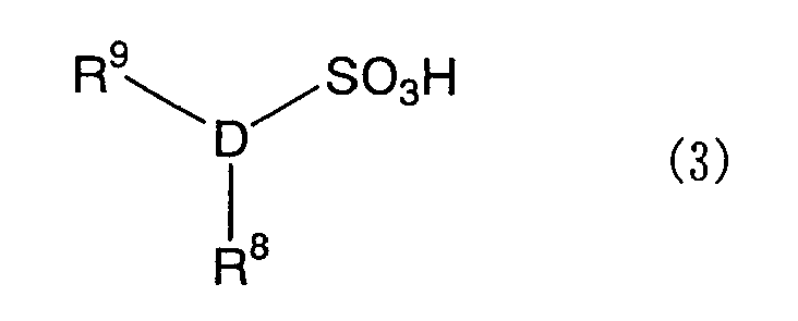
- such compounds include, for example, Tiron, dihydroxybenzenesulfonic acid and sulfonic acid derivatives represented by the formula (3) and the like.
- the sulfonic acid derivatives represented by the formula (3) are preferred.
- Specific examples of the sulfonic acid derivative include sulfosalicyclic acid derivatives, e.g., 5-sulfosalicyclic acid and the like.
- R 8 and R 9 independently represent a carboxyl group or a hydroxyl group.
- the solvent used for obtaining the charge transporting varnish of the invention is not critical provided that it is able to dissolve a charge transporting material having been subjected to oxidation treatment, and it is preferred that the varnish is in a state where completely dissolved or homogeneously dispersed.
- the solvents include water, methanol, N,N-dimethylformamide, N,N-dimethylacetamide, N-methylpyrrolidone, N,N'-dimethylimidazolidinone, dimethylsulfoxide, chloroform, toluene, methanol and the like solvent. These may be used singly or in admixture.
- a highly viscous solvent may be mixed for the purpose of obtaining a varnish having high viscosity within a range of not impeding solubility.
- Specific examples include cyclohexanol, ethylene glycol, ethylene glycol diglycidyl ether, 1,3-octylene glycol, diethylene glycol, dipropylene glycol, triethylene glycol, tripropylene glycol, 1,3-butandiol, 1,4-butandiol, propylene glycol, hexylene glycol and the like although not limited to these solvents.
- solvents for imparting flatness to a film upon firing for the purposes of improving wettability against a substrate, control in surface tension of a solvent, control of polarity, control of a boiling point and the like may be used for the varnish within a range of not impeding solubility.
- Specific examples include butyl cellosolve, diethylene glycol diethyl ether, dipropylene glycol monomethyl ether, ethyl carbitol, diacetone alcohol, ⁇ -butyrolactone, ethyl lactate and the like although not limited to these.
- a concentration of a charge transporting material in a solution can be controlled within the range of 1 to 80 wt%, particularly 1 to 20 wt%.
- a charge transporting film can be formed on a substrate by coating the charge transporting varnish onto the substrate and evaporating the solvent.
- the manner of coating is not limitative, there are mentioned, for example, a dipping method, a spin coating method, a transferring printing method, a roll coating method, an ink jet method, a spraying method, a brushing method and the like.
- the manner of evaporation of solvent is not critical, it is possible to carry out evaporation by use of a hot plate or an oven in an appropriate atmosphere, i.e., in air or an inert gas such as nitrogen or the like, or in vacuum.
- the firing temperature is not critical so far as a solvent can be evaporated and is preferably within 40 to 250°C. To ensure more uniform film formation or to cause the reaction on the substrate to proceed, a temperature may be changed in two or more stages.
- the film thickness is not critical, and preferably ranges 5 to 200 nm where used as a charge injection layer of an organic EL element.
- a method of changing the film thickness mention is made of a method wherein a solid content in a varnish is changed, a method of changing an amount of solution on application to a substrate, and the like.
- the electrode substrate used has been cleaned beforehand through washing with a liquid such as a detergent, an alcohol, pure water or the like, and with an anode substrate, a surface treatment such as an ozone treatment, an oxygen-plasma treatment or the like is carried out immediately before use. It is to be noted that where an anodic material is made principally of an organic matter, the surface treatment may not be performed.
- the hole transporting varnish is applied onto an anode substrate according to such a method as set out above to form a hole transporting thin film on the electrode.
- the substrate is placed into a vacuum evaporation apparatus, followed by successive vacuum deposition of a hole transporting layer, a luminescent layer, an electron transporting layer, an electron injection layer and a cathodic metal to provide an OLED element.
- a carrier block layer may be provided between arbitrary layers.
- ITO indium tin oxide
- IZO indium zinc oxide
- polythiophene derivatives and polyanilines having high charge transportability may also be used.
- triarylamines such as (triphenylamine) dimer derivative (TPD), ( ⁇ -naphthyldiphenylamine) dimer ( ⁇ -NPD), [(triphenylamine)dimer] spirodimer (spiro-TAD) and the like, starburst amines such as 4,4',4"-tris[3-methylphenyl(phenyl)-amino]triphenylamine (m-MTDATA), 4,4',4"-tris[1-naphthyl-(phenyl)amino]triphenylamine (1-TNATA) and the like, and oligothiophenes such as 5,5"-bis-(4-[bis(4-methylphenyl)-amino]phenyl ⁇ -2,2':5',2"terthiophene (BMA-3T) and the like.
- TPD triphenylamine dimer derivative
- ⁇ -NPD ⁇ -naphthyldip
- the luminescent layer may be formed by co-deposition of an electron transporting material or a hole transporting material and a luminescent dopant.
- Alq 3 For an electron transporting material, mention is made of Alq 3 , BAlq, DPVBi, (2-(4-biphenyl)-5-(4-t-butylphenyl)-1,3,4-oxadiazole) (PBD), triazole derivatives (TAZ), baxoproin (BCP), syrol derivatives and the like.
- lithium oxide Li 2 O
- magnesium oxide MgO
- alumina Al 2 O 3
- lithium fluoride LiF
- magnesium fluoride MgF 2
- strontium fluoride SrF 2
- Liq Li(acac)
- lithium acetate lithium benzoate and the like.
- the electron transporting varnish is used to form an electron transporting thin film on an anode substrate and is placed into a vacuum deposition apparatus, and an electron transporting layer, a luminescent layer, a hole transporting layer and a hole injection layer are formed, followed by film formation of an anodic material a method such as sputtering to provide an OLED element.
- the vacuum deposition operations of the hole transporting layer, luminescent layer, electron transporting layer and electron injection layer are not carried out, but a luminescent charge transporting polymer layer is formed thereby making a PLED element including the charge transporting thin film formed of the charge transporting varnish of the present invention.
- the hole transporting varnish is applied onto an anode substrate to form a charge transporting thin film on the electrode according to such a procedure as set out above, on which a luminescent charge transporting polymer layer is formed, followed by vacuum deposition of a cathode electrode to provide a PLED element.
- the electron transporting varnish is applied onto a cathode substrate to form an electron transporting thin film on the electrode according to such a procedure as set out above, followed by forming a luminescent charge transporting polymer layer thereon and forming an anode electrode by a procedure such as sputtering, vacuum deposition, spin coating or the like, thereby providing a PLED element.
- the cathode and anode materials used are those substances as used for fabrication of the above OLED element.
- a washing treatment and a surface treatment in the fabrication of the OLED element can be applied to the fabrication of the PLED element.
- the luminescent charge transporting polymer layer For the formation of the luminescent charge transporting polymer layer, there is mentioned a method wherein a solvent is added to a luminescent charge transporting polymer material or its mixture with a luminescent dopant for dissolution or homogeneous dispersion, followed by coating onto an electrode substrate on which the hole injection layer has been formed, and evaporating the solvent to form a film.
- luminescent charge transporting polymer materials mention is made of polyfluorene derivatives such as poly(9,9-dialkylfluorene)(PDAF) and the like, polyphenylenevinylene derivatives such as poly(2-methoxy-5-(2'-ethylhexoxy)-1,4-phenylenevinylene) (MEH-PPV) and the like, polythiophene derivatives such as poly(3-alkylthiophene) (PAT) and the like, and polyvinylcarbazole (PVCz) and the like.
- polyfluorene derivatives such as poly(9,9-dialkylfluorene)(PDAF) and the like
- polyphenylenevinylene derivatives such as poly(2-methoxy-5-(2'-ethylhexoxy)-1,4-phenylenevinylene) (MEH-PPV) and the like
- polythiophene derivatives such as poly(3-alkylthiophene) (
- the solvents include toluene, xylene, chloroform and the like, and for dissolution or homogeneous dispersion, there are mentioned dissolution or homogeneous dispersion methods including stirring, stirring under heat, ultrasonic dispersion and the like.
- the manner of coating is not critical and includes, for example, a dipping method, a spin coating method, a transferring printing method, a roll coating method, an ink jet method, a spraying method, a brushing method and the like. These coating methods is favorably carried out in an inert gas such as nitrogen, argon or the like.
- phenylpentaaniline (PPA) represented by the formula (4) was obtained through the reaction between p-diaminodiphenylamine and p-hydroxydiphenylamine.
- the synthesis of PPA was carried out according to the following procedure. That is, 1.00 g of p-diaminodiphenylamine was dissolved in 21 ml of toluene, to which 10.21 g of tetra-n-butoxy titanium serving as a dehydration condensing agent was added and dissolved. While the resulting reaction solution was maintained at 110°C under a nitrogen atmosphere, 2.22 g of p-hydroxydiphenylamine dissolved in 42 ml of toluene was added to, followed by reaction at 110°C under a nitrogen atmosphere for 48 hours. After completion of the reaction, the reaction solution cooled down to room temperature was filtered and the resulting filtrate was washed with toluene and then with diethyl ether and dried to obtain a light purple powder.
- the thus obtained powder was dissolved by adding 40 parts of dioxane and 0.2 equivalents of hydrazine hydrate thereto, purging the reaction system with nitrogen and heating under reflux. 16 parts of toluene was added to the resulting solution to suspend the solution, followed by heating under reflux and filtering the resulting solution in a hot condition.
- the solid precipitated from the filtrate was recrystallized, washed successively with toluene-dioxane (1:2.5) and ether under a nitrogen atmosphere, followed by collection through filtration and drying the resulting crystals under reduced pressure at 60°C for 10 hours. Similar recrystallization operations were repeated once more to obtain 2.07 g (with a yield of 64%) of bluish purple crystals.
- the infrared absorption spectrum of the thus obtained PPA is shown in Fig. 1.
- the absorption attributed to the N-H stretch vibration was observed in the vicinity of 3400 cm -1 .
- a mass peak of m/z 533.18 corresponding to the molecular weight of PPA was observed.
- the synthesized PPA was oxidized in the following way. That is, 1.00 g of PPA was dissolved in a mixed solvent of 300 ml of toluene and 50 ml of dioxane, followed by stirring at 110°C in air for 48 hours to oxidize PPA. The resulting black liquid was filtered, and the solvent was distilled off from the filtrate to obtain 0.93 g (yield: 93%) of black powder.
- the infrared absorption spectrum of the resulting oxidized PPA is shown in Fig. 2.
- the N-H stretch vibration at 3400 cm -1 observed in Fig. 1 is reduced in intensity in Fig. 2.
- the substrate was placed into a vacuum deposition apparatus, followed by vacuum deposition of ⁇ -NPD, Alq 3 , LiF and Al successively.
- the film thicknesses were, respectively, set at 40 nm, 60 nm, 0.5 nm and 100 nm, and the vacuum deposition operations were, respectively, carried out after a pressure was at 8 ⁇ 10 -4 Pa or below.
- the deposition rate was 0.3 to 0.4 nm/s except for LiF, and was 0.02 to 0.04 nm/s for LiF.
- the movement operations between the vacuum deposition operation cycles were performed in vacuum.
- 5-Sulfosalicyclic acid (5-SSA), and N,N-dimethylacetamide (DMAc) and cyclohexanol were added to the PPA obtained after synthesis and purification carried by use of the method described in Example 1 to prepare a varnish.
- Example 1 An ITO glass substrate was subjected to ozone cleaning for 40 minutes immediately before spin coating of the varnish.
- the varnish was coated onto the ITO glass substrate according to the method set out in Example 1, followed by firing in air at 160°C and 180°C to provide a 30 nm thick thin film.
- the firing temperature and firing time in the course of film formation, and electric conductivity at room temperature are shown in Table 3. It will be seen that Example 1 ensures the formation of a thin film of higher electric conductivity by firing within a shorter time or at a lower temperature than Comparative Example 1. Table 3 Run No.
- Firing temperature (°C) Firing time (minutes) Electric conductivity [S/cm] (under current application of 100 mA/cm 2 ) 10 180 1 4.66 ⁇ 10 -8 11 180 3 7.79 ⁇ 10 -8 12 180 5 8.79 ⁇ 10 -8 13 180 10 1.02 ⁇ 10 -7 14 180 20 2.93 ⁇ 10 -7 15 180 30 3.99 ⁇ 10 -7 16 180 60 5.36 ⁇ 10 -7 17 180 120 6.98 ⁇ 10 -7 18 160 60 5.93 ⁇ 10 -8
- Example 2 ensures the fabrication of an organic EL element with a higher luminescence initiating voltage and higher efficiency by firing within a shorter time or at a lower temperature than Comparative Example 2.
Landscapes
- Chemical & Material Sciences (AREA)
- Physics & Mathematics (AREA)
- Engineering & Computer Science (AREA)
- Materials Engineering (AREA)
- Organic Chemistry (AREA)
- Health & Medical Sciences (AREA)
- Chemical Kinetics & Catalysis (AREA)
- Medicinal Chemistry (AREA)
- Polymers & Plastics (AREA)
- Spectroscopy & Molecular Physics (AREA)
- Optics & Photonics (AREA)
- Electroluminescent Light Sources (AREA)
Abstract
Description
- This invention relates to a charge-transporting varnish and, more particularly, to a charge-transporting varnish capable of forming, for example, a charge transporting thin film which is able to improve electric characteristics and life characteristic while preventing concentration phenomena of electric current and charge. This charge-transporting varnish is applicable as an organic electroluminescent (hereinafter referred to as EL) element, a capacitor element, an antistatic film and the like.
- Organic EL elements, particularly, low molecular weight organic EL (hereinafter referred to as OLED), have been isolated function thereof by Eastman Kodak based on ultrathinning and multilayering of organic layers and are thus remarkably improved in characteristics such as drastic lowering of drive voltage (Applied Physics Letters, U.S.A., 1987, Vol. 51, pp. 913-915). Cambridge University found an EL element using a polymeric fluorescent material (hereinafter referred to as PLED) (Nature, England, 1990, Vol. 347, pp. 539-541), which has now been improved in characteristics to such a level as to compare with conventional OLED elements.
- On the other hand, it was found that with OLED elements, provision of a copper phthalocyanine (CuPC) layer as a hole injection layer leads to an improvement in initial characteristics such as low drive voltage and high luminous efficiency and an effect of prolonging the life of the elements (Applied Physic Letters, U.S.A., 1996, Vol. 69, pp. 2160-2162). With PLED elements, it has been shown that similar effects are obtained using, as a hole transporting layer (buffer layer), polyaniline materials (Nature, England, 1992, Vol. 357, pp. 477-479, Applied Physics Letters, U.S.A., 1994, Vol. 64, pp. 1245-1247), and polythiophene materials (Applied Physics Letters, U.S.A., 1998, Vol. 72, pp. 2660-2662). At a cathode side, it has been found that initial characteristics could be improved using, as an electron injection layer, metal oxides (IEEE Transactions on Electron Devices, U.S.A., 1997, Vol. 44, pp. 1245-1248), metal halides (Applied Physics Letters, U.S.A., 1997, Vol. 70, pp. 152-154), and metal complexes (Japanese Journal of Applied Physics, 1999, Vol. 38, pp. L1348-1350). These electron layer and buffer layer have been now in general use.
- However, CuPC that has been ordinarily used as a hole injection material in OLED element has the drawback that it has drastic irregularities and thus, brings about a great characteristic lowering upon mixing in other organic layers in small amount. Polyaniline-type materials and polythiophene-type materials currently employed for PLED element involve problems in that they contain, as a solvent, water having capability of promoting element deterioration, limitation is placed on the choice of solvent, limitation is also placed on the manner of coating ensuring uniform film formation because of coagulation of material and low solubility, and a difficulty is involved in control of viscosity.
- Based on the facts set out hereinabove, organic solvent-based charge transporting varnishes using low molecular weight oligoaniline materials have been recently found. It has been found that insertion of a hole injection layer obtained by use of this type of material enables excellent EL element characteristics to be shown (see JP-A 2002-151272).
- In forming a charge transporting thin film from an oligoaniline compound, however, long-time firing at high temperature in the presence of oxygen is usually necessary. Thus, where low molecular weight oligoaniline materials are used as a hole injection layer in OLED element or PLED element, a prolonged time is required for the fabrication of the element, so that a problem has been indicated in the lowering of productivity. Hence, there is a demand for shortage of a firing time after the film formation.
- An object of the invention is to provide a charge transporting varnish capable of achieving excellent conduction characteristics and obtained through firing within a short time in a system using an oligoaniline compound and a charge accepting dopant material.
- As a result of intensive studies for achieving the above object, we have found that when using a charge transporting varnish obtained by dissolving or homogeneously dispersing, in a solvent, a charge transporting material being an oligoaniline compound of the following formula (1), a thin film having conduction characteristics that are as good as a conventional counterpart can be formed only by firing within a short time after film formation.
- More particularly, the present invention provides the following inventions [1] to [8].
- [1] A charge-transporting varnish, characterized by comprising a charge transporting substance being an oligoaniline compound represented by the formula (1) and at least one solvent, the charge transporting substance is dissolved or homogeneously dispersed in said solvent.

- [2] The charge-transporting varnish of [1], characterized in that the charge transporting substance is a product obtained by oxidizing an oligoaniline compound represented by the formula (2).

- [3] The charge-transporting varnish of [1] or [2], characterized by further comprising a charge accepting dopant substance, the oxidized product and the charge accepting dopant being dissolved or homogeneously dispersed in said solvent.
- [4] The charge-transporting varnish of [3], characterized in that the charge accepting dopant substance is a sulfonic acid derivative represented by the formula (3).

- [5] An organic electroluminescent element obtained from the charge-transporting varnish of any one of [1] to [4].
- [6] An organic electroluminescent element comprising a hole injection layer formed from the charge-transporting varnish of any one of [1] to [4].
- [7] An organic electroluminescent element comprising a hole-transporting layer formed from the charge-transporting varnish of any one of [1] to [4].
- [8] A charge transporting thin film formed from the charge-transporting varnish of any one of [1] to [4].
- When using a charge transporting varnish of the invention, a charge transporting thin film can be obtained within a short time without lowering productivity according to a simple, inexpensive wet process. In this connection, the charge transporting varnish of the invention differs from a conventionally employed charge transporting varnish in the form of an aqueous solution, and can be used only by use of an organic solvent.
- The formation of a charge transporting thin film of the invention on an electrode surface can prevent electric short-circuiting. The use of the charge transporting thin film as a charge injection layer of an organic EL element permits injection barrier to lower owing to the relaxation of ionization potentials of an electrode and an organic layer. In addition, application of conjugated oligomer groups to an organic EL element is enabled. From the foregoing, lowering of luminescence initiating voltage of an organic EL element, improvement of a current efficiency and prolonged life can be achieved.
- Further, the charge transporting varnish of the invention is good with respect to thin film formation process and is useful for application to a capacitor electrode protection film and also to an antistatic film.
-
- Fig. 1 is an infrared absorption spectral chart of phenylpentaaniline synthesized in Example 1.
- Fig. 2 is an infrared absorption spectral chart of oxidized phenylpentaaniline synthesized in Example 1.
- The invention is described in more detail below.
- The charge transporting varnish of the invention is one which contains a charge transporting material serving as a principal component for charge transporting mechanism and a solvent, or which contains a charge transporting material, a charge accepting dopant material for improving charge transportability and a solvent. In this case, the charge transporting material (and the charge accepting dopant material) are completely dissolved or homogeneously dispersed in the solvent.
- The transportability used herein has the same meaning as conductivity and means any one of hole transportability, electron transportability, and transportability of both hole and electron. The charge transporting varnish of the invention may exhibit charge transportability in itself, or may exhibit charge transportability after conversion to a solid film obtained by use of the varnish.
- The charge transporting material used in the present invention is an oligoaniline compound represented by the formula (1).

- The substituent R1 of the oligoaniline compound used in the invention is hydrogen, an unsubstituted or substituted monovalent hydrocarbon group, an organooxy group, or an acyl group, and R2 and R3 independently represent a hydrogen atom, an unsubstituted or substituted monovalent hydrocarbon group, or an acyl group.
- The monovalent hydrocarbon group and the organooxy group should preferably have 1 to 20 carbon atoms, and the acyl group should preferably have 2 to 20 carbon atoms. The monovalent hydrocarbon group includes, for example, an alkyl group such as a methyl group, an ethyl group, a propyl group, a butyl group, a t-butyl group, a hexyl group, an octyl group, an decyl group or the like, a cycloalkyl group such as a cyclopentyl group, a cyclohexyl group or the like, a bicycloalkyl group such as a bicyclohexyl group or the like, an alkenyl group such as a vinyl group, a 1-propenyl group, a 2-propenyl group, an isopropenyl group, a 1-methyl-2-propenyl group, a 1, 2 or 3-butenyl group, a hexenyl group or the like, an aryl group such as a phenyl group, a xylyl group, a tolyl group, a biphenyl group, a naphthyl group or the like, an aralkyl group such as a benzyl group, a phenylethyl group, a phenylcyclohexyl group or the like, or a group wherein part or all of the hydrogen atoms of these monovalent hydrocarbon groups are substituted with a halogen atom, a hydroxyl group, an alkoxy group or the like.
- As an organooxy group includes an alkoxy group, an alkenyloxy group, an aryloxy group or the like. For these alkyl group, alkenyl group and aryl group, mention is made of such groups as exemplified above.
- The acyl group includes one having 2 to 10 carbon atoms such as, for example, an acetyl group, a propionyl group, a butyryl group, an isobutyryl group, a valeryl group, an isovaleryl group, a benzyl group or the like.
- Preferred examples of R1 and R2 include a hydrogen atom, an alkyl group having 1 to 20 carbon atoms, preferably 1 to 4 carbon atoms, a phenyl group, a cyclohexyl group, a cyclopentyl group, a biphenyl group, a bicyclohexyl group or a phenylcyclohexyl group (provided these phenyl, cyclohexyl, cyclopentyl, biphenyl, bicyclohexyl and phenylcyclohexyl groups may have a substituent such as an alkyl group or an alkoxy group having 1 to 4 carbon atoms.), or an acyl group having 2 to 4 carbon atoms. For R3, a hydrogen atom, an alkyl group having 1 to 4 carbon atoms, or a phenyl group which may have an alkoxy group as a substituent is preferred.
- Especially, the case where R1 is a hydrogen atom and R3 is a phenyl group, i.e., the oligoaniline compound of the formula (1) is blocked with a phenyl group at both ends thereof, is preferred.
- The substituents R4 to R7 independently represent a hydrogen atom, a hydroxyl group, an unsubstituted or substituted monovalent hydrocarbon group, an organooxy group, an acyl group, and a sulfonic acid group. The unsubstituted or substituted monovalent hydrocarbon group and organooxy group should preferably have 2 to 20 carbon atoms, respectively, and the acyl group should preferably have 2 to 20 carbon atoms, and mention may be made of those groups as indicated with respect to R1.
- The substituents R4 to R7 preferably include a hydrogen atom, an alkyl group, an alkoxy group, an alkoxyalkyl group, an alkenyl group, an acyl group, a sulfonic acid group, and a hydroxyl group, or a phenyl group, a cyclohexyl group, a cyclopentyl group, a biphenyl group, a bicyclohexyl group or a phenylcyclohexyl group that may have a substituent of an alkyl group or alkoxy group each having 1 to 4 carbon atoms.
- More preferably, R4 to R7 represents a hydrogen atom, an alkyl group having 1 to 20 carbon atoms, an alkoxy group having 1 to 20 carbon atoms, an alkoxyalkyl group wherein the alkoxy group has 1 to 20 carbon atoms and the alkyl group has 1 to 20 carbon atoms, an alkenyl group having 2 to 4 carbon atoms, an acyl group having 2 to 4 carbon atoms, a benzoyl group, a sulfonic acid group, a hydroxyl group, or a phenyl group, a cyclohexyl group, a cyclopentyl group, a biphenyl group, a bicyclohexyl group or a phenylcyclohexyl group that may have a substituent (wherein the substituent includes an alkyl group having 1 to 4 carbon atoms or an alkoxy group having 1 to 4 carbon atoms), respectively. Most preferably, mention is made of a hydrogen atom, an alkyl group having 1 to 4 carbon atoms, an alkoxy group having 1 to 4 carbon atoms, an alkoxyalkyl group wherein the alkoxy group has 1 to 4 carbon atoms and the alkyl group has 1 to 4 carbon atom, a vinyl group, a 2-propenyl group, an acetyl group, a benzoyl group, a sulfonic acid group, a hydroxyl group, or a phenyl group, a cyclohexyl group, a biphenyl group, a bicyclohexyl group or a phenylcyclohexyl group that may have a substituent (wherein the substituent includes an alkyl group having 1 to 4 carbon atoms or an alkoxy group having 1 to 4 carbon atoms), respectively. It will be noted that in the two benzene rings of the formula (1), the substituents indicated by the same symbol may be the same or different.
- The numbers of m and n at the oligoaniline moiety are independently an integer of 1 or over. It is preferred that a ratio of m to n is 2 or over. Where solubility in a solvent for charge transporting material is taken into account, m+2n should preferably be 20 or below. Where a solution having a high concentration of 20 wt% or over is prepared, a value of 10 or below, preferably 5 or below is preferred.
- The charge transporting material of the formula (1) can be obtained by oxidizing an oligoaniline compound of the formula (2).

- When taking enhanced solubility and uniform charge transportability into account, the oligoaniline compound represented by the formula (2) should preferably one which has no distribution of molecular weight, i.e., a degree of dispersion is at 1.
- Specific examples of such an oligoaniline compound are those oligoaniline compounds soluble in organic solvents, such as phenyltetraaniline, phenylpentaaniline and the like. With respect to the synthesis of this type of oligoaniline compound, mention is made of synthetic processes set forth, for example, in Bulletin of Chemical Society of Japan, 1994, Vol. 67, pp. 1749-1752) and Synthetic Metals, U.S.A., 1997, Vol. 84, pp. 119-120) although not limited to these ones.
- The oxidation treatment carried out for the oligoaniline compound of the formula (2) is performed by a procedure wherein after dissolving the oligoaniline compound in an appropriate solvent, for example, chemical oxidation is carried out by use of an appropriate oxidizing agent, or wherein while heating a powder or solution of the oligoaniline compound, oxidation is carried out in air or in the presence of oxygen under stirring, although not limited to these procedures.
- For the solvent used for carrying out the oxidation treatment, although mention is made specifically of N,N-dimethylformamide, N,N-dimethylacetamide, N-methylpyrrolidone, N,N'-dimethylimidazolidinone, dimethylsulfoxide, chloroform, tetrahydrofuran, 1,4-dioxane, toluene, xylene and the like, no limitation is placed so far as those capable of dissolving the oligoaniline are used. These may be used singly or in admixture.
- Specific examples of an oxidizing agent used for carrying out the oxidation treatment include a halogen such as chlorine, bromine, iodine or the like, an inorganic acid such as nitric acid, sulfuric acid or the like, an inorganic oxidizing agent such as ozone, hydrogen peroxide, potassium permanganate, potassium dichromate, sulfur dioxide and the like, and organic oxidizing agent such as 7,7,8,8-tetacyaoquinodimethane (TCNQ) and derivatives thereof, 1,1,2,2-tetracyanoethylene (TCNE), 2,3-dichloro-5,6-dicyano-1,4-enzoquinone (DDQ), chloranil and bromanil although not limited to these compounds.
- As the charge accepting dopant material used in the invention, an electron accepting dopant material is used for a hole transporting material and a hole accepting dopant material is used for an electron transporting material, and both should favorably have high charge receptivity. As to solubility, no limitation is placed so far as those materials capable of being dissolved in at least one solvent are used.
- Specific examples of the electron accepting dopant include inorganic strong acids such as hydrogen chloride, sulfuric acid, nitric acid and phosphoric acid, Lewis acids such as aluminium (III) chloride (AlCl3), titanium (IV) tetrachloride (TiCL), boron tribromide (BBr3), borontrifluoride complex (BF3OEt2), iron (III) chloride (FeCl3), copper (II) chloride (CuCl2), antimony pentachloride (SbCl5), arsenic (V) pentafluoride (AsF5), phosphorus pentafluoride (PF5), tri(4-bromophenyl)aluminium hexachloroantmonate ((TBPAH) and the like, organic strong acids such as benzenesulfonic acid, tosyl acid, camphorsulfonic acid, hydroxybenzensulfonic acid, 5-sulfosalicylic acid, dodecylbenzenesulfonic acid, polystyrenesulfonic acid and the like, and organic or inorganic oxidizing agents such as TCNQ and derivatives thereof, DDQ and iodine although not limited to these compounds.
- Specific examples of the hole accepting dopants include alkali metals (Li, Na, K, Cs) and metal complexes such as lithium quinolinoate (Liq) and lithium acetylacetonate (Li(acac)), and the like although not limited to these dopants. Both of the charge transporting material and charge accepting dopant material should preferably be in the form of an amorphous solid. If either or both are not in the form of an amorphous solid, it has found as a result of combination of both the charge transporting material and charge accepting dopant substance and a solvent indicated hereinafter that materials capable of exhibiting an amorphous solid property after film formation are preferred. Where either or both of the charge transporting material and charge accepting dopant material are in the form of a crystalline solid, at least one of the materials should preferably have random intermolecular interaction. With a low molecular weight compound, those materials having, for example, three or more different polar functional groups in the same molecule are favorable. Although not limitative, such compounds include, for example, Tiron, dihydroxybenzenesulfonic acid and sulfonic acid derivatives represented by the formula (3) and the like. Of these, the sulfonic acid derivatives represented by the formula (3) are preferred. Specific examples of the sulfonic acid derivative include sulfosalicyclic acid derivatives, e.g., 5-sulfosalicyclic acid and the like.

- The solvent used for obtaining the charge transporting varnish of the invention is not critical provided that it is able to dissolve a charge transporting material having been subjected to oxidation treatment, and it is preferred that the varnish is in a state where completely dissolved or homogeneously dispersed. Specific examples of the solvents include water, methanol, N,N-dimethylformamide, N,N-dimethylacetamide, N-methylpyrrolidone, N,N'-dimethylimidazolidinone, dimethylsulfoxide, chloroform, toluene, methanol and the like solvent. These may be used singly or in admixture.
- A highly viscous solvent may be mixed for the purpose of obtaining a varnish having high viscosity within a range of not impeding solubility. Specific examples include cyclohexanol, ethylene glycol, ethylene glycol diglycidyl ether, 1,3-octylene glycol, diethylene glycol, dipropylene glycol, triethylene glycol, tripropylene glycol, 1,3-butandiol, 1,4-butandiol, propylene glycol, hexylene glycol and the like although not limited to these solvents.
- Further, solvents for imparting flatness to a film upon firing for the purposes of improving wettability against a substrate, control in surface tension of a solvent, control of polarity, control of a boiling point and the like may be used for the varnish within a range of not impeding solubility. Specific examples include butyl cellosolve, diethylene glycol diethyl ether, dipropylene glycol monomethyl ether, ethyl carbitol, diacetone alcohol, γ-butyrolactone, ethyl lactate and the like although not limited to these.
- A concentration of a charge transporting material in a solution can be controlled within the range of 1 to 80 wt%, particularly 1 to 20 wt%.
- A charge transporting film can be formed on a substrate by coating the charge transporting varnish onto the substrate and evaporating the solvent. Although the manner of coating is not limitative, there are mentioned, for example, a dipping method, a spin coating method, a transferring printing method, a roll coating method, an ink jet method, a spraying method, a brushing method and the like. Although the manner of evaporation of solvent is not critical, it is possible to carry out evaporation by use of a hot plate or an oven in an appropriate atmosphere, i.e., in air or an inert gas such as nitrogen or the like, or in vacuum. The firing temperature is not critical so far as a solvent can be evaporated and is preferably within 40 to 250°C. To ensure more uniform film formation or to cause the reaction on the substrate to proceed, a temperature may be changed in two or more stages.
- With respect to the charge transporting thin film obtained by the coating and evaporation procedures, the film thickness is not critical, and preferably ranges 5 to 200 nm where used as a charge injection layer of an organic EL element. For a method of changing the film thickness, mention is made of a method wherein a solid content in a varnish is changed, a method of changing an amount of solution on application to a substrate, and the like.
- The procedure of making an OLED element using the charge transporting varnish of the invention and the types of materials used may be those described hereinbelow although not limited thereto.
- It is preferred that the electrode substrate used has been cleaned beforehand through washing with a liquid such as a detergent, an alcohol, pure water or the like, and with an anode substrate, a surface treatment such as an ozone treatment, an oxygen-plasma treatment or the like is carried out immediately before use. It is to be noted that where an anodic material is made principally of an organic matter, the surface treatment may not be performed.
- Where a hole transporting varnish is used for an OLED element, the following procedure is used.
- The hole transporting varnish is applied onto an anode substrate according to such a method as set out above to form a hole transporting thin film on the electrode. The substrate is placed into a vacuum evaporation apparatus, followed by successive vacuum deposition of a hole transporting layer, a luminescent layer, an electron transporting layer, an electron injection layer and a cathodic metal to provide an OLED element. For controlling a luminescent region, a carrier block layer may be provided between arbitrary layers.
- Mention is made, as an anodic material, transparent electrodes typical of which are indium tin oxide (ITO) and indium zinc oxide (IZO), and it is preferred to use those subjected to planarization. Alternatively, polythiophene derivatives and polyanilines having high charge transportability may also be used. For materials forming a hole transporting layer, there are mentioned triarylamines such as (triphenylamine) dimer derivative (TPD), (α-naphthyldiphenylamine) dimer (α-NPD), [(triphenylamine)dimer] spirodimer (spiro-TAD) and the like, starburst amines such as 4,4',4"-tris[3-methylphenyl(phenyl)-amino]triphenylamine (m-MTDATA), 4,4',4"-tris[1-naphthyl-(phenyl)amino]triphenylamine (1-TNATA) and the like, and oligothiophenes such as 5,5"-bis-(4-[bis(4-methylphenyl)-amino]phenyl}-2,2':5',2"terthiophene (BMA-3T) and the like.
- For the material forming a luminescent layer, mention is made of tris(8-quinolinolate) aluminium (III) (Alq3), bis(8-quinolinolate) zinc (II) (Znq2), bis(2-methyl-8-quinolinolate)(p-phenylphenolate) aluminium (III) (BAlq), 4,4'-bis(2,2-diphenylvinyl)biphenyl (DPVBi) and the like. The luminescent layer may be formed by co-deposition of an electron transporting material or a hole transporting material and a luminescent dopant.
- For an electron transporting material, mention is made of Alq3, BAlq, DPVBi, (2-(4-biphenyl)-5-(4-t-butylphenyl)-1,3,4-oxadiazole) (PBD), triazole derivatives (TAZ), baxoproin (BCP), syrol derivatives and the like.
- For a luminescent dopant, mention is made of quinacridone, rubrene, coumarin 540, 4-(dicyanomethylene)-2-methyl-6-(p-dimethylaminostyryl)-4H-pyran (DCM), tris(2-phenylpyridine) iridium (III) (Ir(ppy)3), (1,10-phenanthoroline)-tris(4,4,4-trifluoro-1-(2-thienyl)-butan-1,3-dionate)europium (III) (Eu(TTA)3phen) and the like.
- For a material forming a carrier block layer, PBD, TAZ and BCP are mentioned.
- For an electron injection layer, mention is made of lithium oxide (Li2O), magnesium oxide (MgO), alumina (Al2O3), lithium fluoride (LiF), magnesium fluoride (MgF2), strontium fluoride (SrF2), Liq, Li(acac), lithium acetate, lithium benzoate and the like.
- Aluminium, magnesium-silver alloys, aluminium-lithium alloys, lithium, sodium, potassium, cesium and the like are mentioned as a cathodic material.
- With the case where the charge transporting varnish of the invention is used as an OLED element, the following procedure is employed.
- The electron transporting varnish is used to form an electron transporting thin film on an anode substrate and is placed into a vacuum deposition apparatus, and an electron transporting layer, a luminescent layer, a hole transporting layer and a hole injection layer are formed, followed by film formation of an anodic material a method such as sputtering to provide an OLED element.
- Although the manner of making a PLED element using the charge transporting varnish of the invention is not critical, mention is made of the following procedure.
- In the fabrication of the above OLED element, the vacuum deposition operations of the hole transporting layer, luminescent layer, electron transporting layer and electron injection layer are not carried out, but a luminescent charge transporting polymer layer is formed thereby making a PLED element including the charge transporting thin film formed of the charge transporting varnish of the present invention. More particularly, the hole transporting varnish is applied onto an anode substrate to form a charge transporting thin film on the electrode according to such a procedure as set out above, on which a luminescent charge transporting polymer layer is formed, followed by vacuum deposition of a cathode electrode to provide a PLED element. Alternatively, the electron transporting varnish is applied onto a cathode substrate to form an electron transporting thin film on the electrode according to such a procedure as set out above, followed by forming a luminescent charge transporting polymer layer thereon and forming an anode electrode by a procedure such as sputtering, vacuum deposition, spin coating or the like, thereby providing a PLED element.
- The cathode and anode materials used are those substances as used for fabrication of the above OLED element. A washing treatment and a surface treatment in the fabrication of the OLED element can be applied to the fabrication of the PLED element.
- For the formation of the luminescent charge transporting polymer layer, there is mentioned a method wherein a solvent is added to a luminescent charge transporting polymer material or its mixture with a luminescent dopant for dissolution or homogeneous dispersion, followed by coating onto an electrode substrate on which the hole injection layer has been formed, and evaporating the solvent to form a film.
- For the luminescent charge transporting polymer materials, mention is made of polyfluorene derivatives such as poly(9,9-dialkylfluorene)(PDAF) and the like, polyphenylenevinylene derivatives such as poly(2-methoxy-5-(2'-ethylhexoxy)-1,4-phenylenevinylene) (MEH-PPV) and the like, polythiophene derivatives such as poly(3-alkylthiophene) (PAT) and the like, and polyvinylcarbazole (PVCz) and the like.
- The solvents include toluene, xylene, chloroform and the like, and for dissolution or homogeneous dispersion, there are mentioned dissolution or homogeneous dispersion methods including stirring, stirring under heat, ultrasonic dispersion and the like.
- The manner of coating is not critical and includes, for example, a dipping method, a spin coating method, a transferring printing method, a roll coating method, an ink jet method, a spraying method, a brushing method and the like. These coating methods is favorably carried out in an inert gas such as nitrogen, argon or the like.
- For the evaporation of solvent, there is mentioned a method of heating in an inert gas or in vacuum with an oven or on a hot plate.
- The invention is more particularly described by Examples and Comparative Examples, and the invention should not be construed as limited to the following Examples. It will be noted that "parts" in the following illustration means "parts by weight".
- Referring to the method described in Bulletin of Chemical Society of Japan, 1994, Vol. 67, pp. 1749-1752, phenylpentaaniline (PPA) represented by the formula (4) was obtained through the reaction between p-diaminodiphenylamine and p-hydroxydiphenylamine.

- The synthesis of PPA was carried out according to the following procedure. That is, 1.00 g of p-diaminodiphenylamine was dissolved in 21 ml of toluene, to which 10.21 g of tetra-n-butoxy titanium serving as a dehydration condensing agent was added and dissolved. While the resulting reaction solution was maintained at 110°C under a nitrogen atmosphere, 2.22 g of p-hydroxydiphenylamine dissolved in 42 ml of toluene was added to, followed by reaction at 110°C under a nitrogen atmosphere for 48 hours. After completion of the reaction, the reaction solution cooled down to room temperature was filtered and the resulting filtrate was washed with toluene and then with diethyl ether and dried to obtain a light purple powder.
- The thus obtained powder was dissolved by adding 40 parts of dioxane and 0.2 equivalents of hydrazine hydrate thereto, purging the reaction system with nitrogen and heating under reflux. 16 parts of toluene was added to the resulting solution to suspend the solution, followed by heating under reflux and filtering the resulting solution in a hot condition. The solid precipitated from the filtrate was recrystallized, washed successively with toluene-dioxane (1:2.5) and ether under a nitrogen atmosphere, followed by collection through filtration and drying the resulting crystals under reduced pressure at 60°C for 10 hours. Similar recrystallization operations were repeated once more to obtain 2.07 g (with a yield of 64%) of bluish purple crystals. The infrared absorption spectrum of the thus obtained PPA is shown in Fig. 1. The absorption attributed to the N-H stretch vibration was observed in the vicinity of 3400 cm-1. In the mass spectrum (MALDI-TOF) of the PPA, a mass peak of m/z = 533.18 corresponding to the molecular weight of PPA was observed.
- The synthesized PPA was oxidized in the following way. That is, 1.00 g of PPA was dissolved in a mixed solvent of 300 ml of toluene and 50 ml of dioxane, followed by stirring at 110°C in air for 48 hours to oxidize PPA. The resulting black liquid was filtered, and the solvent was distilled off from the filtrate to obtain 0.93 g (yield: 93%) of black powder.
- The infrared absorption spectrum of the resulting oxidized PPA is shown in Fig. 2. The N-H stretch vibration at 3400 cm-1 observed in Fig. 1 is reduced in intensity in Fig. 2. In the mass spectrum (MALD1-TOF) of the oxidized PPA, mass peaks of m/z = 529.57 and m/z = 531.59, which was smaller than the molecular weight of PPA, were observed. In view of this, it is considered that PPA is reliably oxidized by the above oxidation treatment.
- 0.43 g of 5-sulfosalicyclic acid and 2.8 g of N,N-dimethylacetamide (DMAc) were added to 0.18 g of the thus obtained, oxidized PPA under a nitrogen atmosphere and dissolved. 7.9 g of cyclohexanol was added to the resulting solution and stirred to provide a varnish (solid content: 4.2%). The thin film formation of the resulting varnish on an ITO glass substrate was carried out in the following way. An ozone treatment is carried out for 40 minutes on the ITO glass substrate immediately before a spin coating on the varnish. More particularly, the varnish was coated on the substrate according to a spin coating method and fired in air at 160°C and 180°C to form a 30 nm thick thin film. The firing temperature and firing time in the course of film formation, and electric conductivity at room temperature are shown in Table 1.
Table 1 Run No. Firing temperature (°C) Firing time (minutes) Electric conductivity [S/cm] (under current application of 100 mA/cm2) 1 180 1 3.82 × 10⁻⁷ 2 180 3 5.20 × 10⁻⁷ 3 180 5 6.19 × 10⁻⁷ 4 180 10 6.16 × 10⁻⁷ 5 180 20 6.29 × 10⁻⁷ 6 180 30 6.62 × 10⁻⁷ 7 180 60 6.72 × 10⁻⁷ 8 180 120 7.03 × 10⁻⁷ 9 160 60 1.67 × 10⁻⁷ - After formation of a hole transporting thin film on an ITO glass substrate according to the method set out in Example 1, the substrate was placed into a vacuum deposition apparatus, followed by vacuum deposition of α-NPD, Alq3, LiF and Al successively. The film thicknesses were, respectively, set at 40 nm, 60 nm, 0.5 nm and 100 nm, and the vacuum deposition operations were, respectively, carried out after a pressure was at 8×10⁻⁴ Pa or below. The deposition rate was 0.3 to 0.4 nm/s except for LiF, and was 0.02 to 0.04 nm/s for LiF. The movement operations between the vacuum deposition operation cycles were performed in vacuum. The characteristics of the resulting OLED element are shown in Table 2.
Table 2 Run No. Firing temperature (°C) Firing time (minutes) Luminescence initiating initiating Voltage [V] At the time of luminescence of 500 cd/m2 Voltage [V] Current efficiency [CD/A] 1 180 1 3.5 10.8 2.5 3 180 5 3.5 10.6 3.0 4 180 10 3.3 8.3 3.4 6 180 30 3.0 8.1 3.4 7 180 60 3.0 8.1 3.5 8 180 120 2.8 7.1 4.0 9 160 60 3.0 8.2 3.3 - 5-Sulfosalicyclic acid (5-SSA), and N,N-dimethylacetamide (DMAc) and cyclohexanol were added to the PPA obtained after synthesis and purification carried by use of the method described in Example 1 to prepare a varnish.
- An ITO glass substrate was subjected to ozone cleaning for 40 minutes immediately before spin coating of the varnish. The varnish was coated onto the ITO glass substrate according to the method set out in Example 1, followed by firing in air at 160°C and 180°C to provide a 30 nm thick thin film. The firing temperature and firing time in the course of film formation, and electric conductivity at room temperature are shown in Table 3. It will be seen that Example 1 ensures the formation of a thin film of higher electric conductivity by firing within a shorter time or at a lower temperature than Comparative Example 1.
Table 3 Run No. Firing temperature (°C) Firing time (minutes) Electric conductivity [S/cm] (under current application of 100 mA/cm2) 10 180 1 4.66 × 10⁻⁸ 11 180 3 7.79 × 10⁻⁸ 12 180 5 8.79 × 10⁻⁸ 13 180 10 1.02 × 10⁻⁷ 14 180 20 2.93 × 10⁻⁷ 15 180 30 3.99 × 10⁻⁷ 16 180 60 5.36 × 10⁻⁷ 17 180 120 6.98 × 10⁻⁷ 18 160 60 5.93 × 10⁻⁸ - After formation on an ITO glass substrate as a hole transporting thin film by the method set out in Comparative Example 1, the substrate was placed into a vacuum deposition apparatus, followed by successive vacuum deposition of α-NPD, Alq3, LiF and Al under the same conditions as in the method set out in Example 1. The characteristics of the resulting OLED element are shown in Table 4. Example 2 ensures the fabrication of an organic EL element with a higher luminescence initiating voltage and higher efficiency by firing within a shorter time or at a lower temperature than Comparative Example 2.
Table 4 Run No. Firing temperature (°C) Firing time (minutes) Luminescence initiating voltage [V] At the time of luminescence of 500 cd/m2 Voltage [V] Current efficiency [CD/A] 10 180 1 5.0 14.3 2.1 12 180 5 4.5 13.2 2.3 13 180 10 4.5 10.6 2.4 15 180 30 3.5 8.6 3.1 16 180 60 3.0 8.4 3.5 17 180 120 3.0 8.4 4.0 18 160 60 4.0 8.7 3.1
Claims (8)
- A charge-transporting varnish, characterized by comprising a charge transporting substance being an oligoaniline compound represented by the formula (1) and at least one solvent, the charge transporting substance is dissolved or homogeneously dispersed in said solvent.

- The charge-transporting varnish as set forth in claim 1, characterized in that the charge transporting substance is a product obtained by oxidizing an oligoaniline compound represented by the formula (2).

- The charge-transporting varnish as set forth in claim 1 or 2, characterized by further comprising a charge accepting dopant substance, the oxidized product and the charge accepting dopant being dissolved or homogeneously dispersed in said solvent.
- The charge-transporting varnish as set forth in claim 3, characterized in that the charge accepting dopant substance is a sulfonic acid derivative represented by the formula (3).
- An organic electroluminescent element obtained from the charge-transporting varnish as set forth in any one of claims 1 to 4.
- The organic electroluminescent element comprising a hole injection layer formed from the charge-transporting varnish as set forth in any one of claims 1 to 4.
- The organic electroluminescent element comprising a hole-transporting layer formed from the charge-transporting varnish as set forth in any one of claims 1 to 4.
- A charge transporting thin film formed from the charge-transporting varnish as set forth in any one of claims 1 to 4.
Applications Claiming Priority (2)
| Application Number | Priority Date | Filing Date | Title |
|---|---|---|---|
| JP2003141975 | 2003-05-20 | ||
| PCT/JP2004/007118 WO2004105446A1 (en) | 2003-05-20 | 2004-05-19 | Charge-transporting varnish |
Publications (3)
| Publication Number | Publication Date |
|---|---|
| EP1638372A1 true EP1638372A1 (en) | 2006-03-22 |
| EP1638372A4 EP1638372A4 (en) | 2010-01-20 |
| EP1638372B1 EP1638372B1 (en) | 2014-02-12 |
Family
ID=33475041
Family Applications (1)
| Application Number | Title | Priority Date | Filing Date |
|---|---|---|---|
| EP04733958.5A Expired - Lifetime EP1638372B1 (en) | 2003-05-20 | 2004-05-19 | Charge-transporting varnish |
Country Status (7)
| Country | Link |
|---|---|
| US (1) | US7341678B2 (en) |
| EP (1) | EP1638372B1 (en) |
| JP (1) | JP4561997B2 (en) |
| KR (1) | KR101099020B1 (en) |
| CN (1) | CN100479630C (en) |
| TW (1) | TW200502277A (en) |
| WO (1) | WO2004105446A1 (en) |
Cited By (6)
| Publication number | Priority date | Publication date | Assignee | Title |
|---|---|---|---|---|
| EP1773102A4 (en) * | 2004-04-30 | 2009-11-11 | Nissan Chemical Ind Ltd | Varnish containing good solvent and poor solvent |
| EP1950816A4 (en) * | 2005-10-28 | 2012-02-22 | Nissan Chemical Ind Ltd | CHARGE TRANSPORT VARNISH FOR A SPRAYING OR INKJET PROCESS |
| US8575392B2 (en) | 2006-07-18 | 2013-11-05 | Nissan Chemical Industries, Ltd. | Charge-transporting varnish |
| EP2759574A4 (en) * | 2011-09-21 | 2015-08-12 | Nissan Chemical Ind Ltd | CARGO TRANSPORT PAINT |
| US9172048B2 (en) | 2002-11-07 | 2015-10-27 | Nissan Chemical Industries, Ltd. | Charge-transporting varnish |
| EP3373354A4 (en) * | 2015-11-06 | 2018-12-05 | Nissan Chemical Corporation | Composition for hole trapping layer of organic photoelectric conversion element |
Families Citing this family (11)
| Publication number | Priority date | Publication date | Assignee | Title |
|---|---|---|---|---|
| DE60336710D1 (en) * | 2002-02-20 | 2011-05-26 | Nissan Chemical Ind Ltd | ORGANIC CONDUCTIVE MATERIAL AND CONDUCTIVE PAINT |
| WO2010058777A1 (en) * | 2008-11-19 | 2010-05-27 | 日産化学工業株式会社 | Charge transporting material and charge transporting varnish |
| CN102585218B (en) * | 2012-01-17 | 2013-10-16 | 黑龙江大学 | Polyaniline derivative, preparation method of reductive poly Schiff base of polyaniline derivative and application of polyaniline derivative |
| WO2015050253A1 (en) | 2013-10-04 | 2015-04-09 | 日産化学工業株式会社 | Aniline derivatives and uses thereof |
| EP3056484A4 (en) | 2013-10-09 | 2017-07-05 | Nissan Chemical Industries, Ltd. | Arylsulfonic acid compound, use thereof, and method for producing arylsulfonic acid compound |
| WO2017150412A1 (en) | 2016-03-03 | 2017-09-08 | 日産化学工業株式会社 | Charge-transporting varnish |
| WO2017164158A1 (en) | 2016-03-24 | 2017-09-28 | 日産化学工業株式会社 | Arylamine derivative and use thereof |
| KR102494413B1 (en) * | 2016-12-16 | 2023-02-02 | 닛산 가가쿠 가부시키가이샤 | Composition for hole trapping layer of organic photoelectric conversion device |
| EP3582279A4 (en) | 2017-02-07 | 2020-12-30 | Nissan Chemical Corporation | CARGO TRANSPORTING PAINT |
| WO2018186340A1 (en) | 2017-04-05 | 2018-10-11 | 日産化学株式会社 | Charge-transporting varnish |
| KR102714396B1 (en) | 2017-12-20 | 2024-10-10 | 닛산 가가쿠 가부시키가이샤 | Sulphonic acid ester compounds and their uses |
Family Cites Families (6)
| Publication number | Priority date | Publication date | Assignee | Title |
|---|---|---|---|---|
| US5723873A (en) | 1994-03-03 | 1998-03-03 | Yang; Yang | Bilayer composite electrodes for diodes |
| US6497969B2 (en) | 1997-09-05 | 2002-12-24 | Nessdisplay Co., Ltd. | Electroluminescent device having an organic layer including polyimide |
| JP2000044683A (en) | 1998-07-29 | 2000-02-15 | Nissan Chem Ind Ltd | Diamine having oligo-aniline unit and polyimide |
| AU2001268187A1 (en) * | 2000-06-20 | 2002-01-02 | Dupont Displays, Inc. | High resistance conductive polymers for use in high efficiency pixellated organic electronic devices |
| JP4868099B2 (en) | 2000-11-09 | 2012-02-01 | 日産化学工業株式会社 | Electroluminescent device |
| GB0028317D0 (en) * | 2000-11-21 | 2001-01-03 | South Bank Univ Entpr Ltd | Electroluminescent device incorporating polyaniline |
-
2004
- 2004-05-18 TW TW093113981A patent/TW200502277A/en not_active IP Right Cessation
- 2004-05-19 WO PCT/JP2004/007118 patent/WO2004105446A1/en not_active Ceased
- 2004-05-19 JP JP2005506380A patent/JP4561997B2/en not_active Expired - Fee Related
- 2004-05-19 EP EP04733958.5A patent/EP1638372B1/en not_active Expired - Lifetime
- 2004-05-19 KR KR1020057021736A patent/KR101099020B1/en not_active Expired - Fee Related
- 2004-05-19 CN CNB2004800173289A patent/CN100479630C/en not_active Expired - Lifetime
- 2004-05-19 US US10/557,177 patent/US7341678B2/en not_active Expired - Lifetime
Cited By (8)
| Publication number | Priority date | Publication date | Assignee | Title |
|---|---|---|---|---|
| US9172048B2 (en) | 2002-11-07 | 2015-10-27 | Nissan Chemical Industries, Ltd. | Charge-transporting varnish |
| EP1773102A4 (en) * | 2004-04-30 | 2009-11-11 | Nissan Chemical Ind Ltd | Varnish containing good solvent and poor solvent |
| US9251923B2 (en) | 2004-04-30 | 2016-02-02 | Nissan Chemical Industries, Ltd. | Varnish containing good solvent and poor solvent |
| EP1950816A4 (en) * | 2005-10-28 | 2012-02-22 | Nissan Chemical Ind Ltd | CHARGE TRANSPORT VARNISH FOR A SPRAYING OR INKJET PROCESS |
| US8575392B2 (en) | 2006-07-18 | 2013-11-05 | Nissan Chemical Industries, Ltd. | Charge-transporting varnish |
| EP2759574A4 (en) * | 2011-09-21 | 2015-08-12 | Nissan Chemical Ind Ltd | CARGO TRANSPORT PAINT |
| EP3373354A4 (en) * | 2015-11-06 | 2018-12-05 | Nissan Chemical Corporation | Composition for hole trapping layer of organic photoelectric conversion element |
| US10770659B2 (en) | 2015-11-06 | 2020-09-08 | Nissan Chemical Industries, Ltd. | Composition for hole trapping layer of organic photoelectric conversion element |
Also Published As
| Publication number | Publication date |
|---|---|
| WO2004105446A1 (en) | 2004-12-02 |
| US20060225611A1 (en) | 2006-10-12 |
| US7341678B2 (en) | 2008-03-11 |
| CN1810064A (en) | 2006-07-26 |
| EP1638372B1 (en) | 2014-02-12 |
| TWI324620B (en) | 2010-05-11 |
| EP1638372A4 (en) | 2010-01-20 |
| TW200502277A (en) | 2005-01-16 |
| CN100479630C (en) | 2009-04-15 |
| KR101099020B1 (en) | 2011-12-28 |
| JP4561997B2 (en) | 2010-10-13 |
| KR20060003101A (en) | 2006-01-09 |
| JPWO2004105446A1 (en) | 2006-07-20 |
Similar Documents
| Publication | Publication Date | Title |
|---|---|---|
| JP4591681B2 (en) | Charge transport varnish | |
| JP5590168B2 (en) | Oligoaniline compounds | |
| EP2062871B1 (en) | Oligoaniline compound and use thereof | |
| EP2042484B1 (en) | Charge-transporting varnish | |
| JP4811573B2 (en) | Charge-transporting organic material containing a compound having a 1,4-dithiine ring | |
| JP5024498B2 (en) | Charge transporting varnish, charge transporting thin film, and organic electroluminescence device | |
| EP1638372B1 (en) | Charge-transporting varnish | |
| KR101016267B1 (en) | Organic conductive materials and conductive varnishes | |
| EP1905804B1 (en) | Charge-transporting varnishes containing charge-transporting polymers and organic electroluminescent devices made by using the same | |
| EP3498740A1 (en) | Coating composition, method for producing organic electroluminescent device using same, and organic electroluminescent device produced thereby | |
| JP4375502B2 (en) | Light emitting element |
Legal Events
| Date | Code | Title | Description |
|---|---|---|---|
| PUAI | Public reference made under article 153(3) epc to a published international application that has entered the european phase |
Free format text: ORIGINAL CODE: 0009012 |
|
| 17P | Request for examination filed |
Effective date: 20051206 |
|
| AK | Designated contracting states |
Kind code of ref document: A1 Designated state(s): AT BE BG CH CY CZ DE DK EE ES FI FR GB GR HU IE IT LI LU MC NL PL PT RO SE SI SK TR |
|
| DAX | Request for extension of the european patent (deleted) | ||
| A4 | Supplementary search report drawn up and despatched |
Effective date: 20091223 |
|
| RIC1 | Information provided on ipc code assigned before grant |
Ipc: H01L 51/00 20060101ALI20091217BHEP Ipc: H01L 51/50 20060101ALI20091217BHEP Ipc: H05B 33/22 20060101AFI20041208BHEP |
|
| 17Q | First examination report despatched |
Effective date: 20100429 |
|
| GRAP | Despatch of communication of intention to grant a patent |
Free format text: ORIGINAL CODE: EPIDOSNIGR1 |
|
| INTG | Intention to grant announced |
Effective date: 20131004 |
|
| GRAP | Despatch of communication of intention to grant a patent |
Free format text: ORIGINAL CODE: EPIDOSNIGR1 |
|
| GRAS | Grant fee paid |
Free format text: ORIGINAL CODE: EPIDOSNIGR3 |
|
| INTG | Intention to grant announced |
Effective date: 20131209 |
|
| GRAA | (expected) grant |
Free format text: ORIGINAL CODE: 0009210 |
|
| RBV | Designated contracting states (corrected) |
Designated state(s): DE FR GB |
|
| AK | Designated contracting states |
Kind code of ref document: B1 Designated state(s): DE FR GB |
|
| REG | Reference to a national code |
Ref country code: GB Ref legal event code: FG4D |
|
| REG | Reference to a national code |
Ref country code: DE Ref legal event code: R096 Ref document number: 602004044380 Country of ref document: DE Effective date: 20140320 |
|
| REG | Reference to a national code |
Ref country code: DE Ref legal event code: R097 Ref document number: 602004044380 Country of ref document: DE |
|
| PLBE | No opposition filed within time limit |
Free format text: ORIGINAL CODE: 0009261 |
|
| STAA | Information on the status of an ep patent application or granted ep patent |
Free format text: STATUS: NO OPPOSITION FILED WITHIN TIME LIMIT |
|
| 26N | No opposition filed |
Effective date: 20141113 |
|
| REG | Reference to a national code |
Ref country code: DE Ref legal event code: R097 Ref document number: 602004044380 Country of ref document: DE Effective date: 20141113 |
|
| REG | Reference to a national code |
Ref country code: FR Ref legal event code: PLFP Year of fee payment: 13 |
|
| REG | Reference to a national code |
Ref country code: FR Ref legal event code: PLFP Year of fee payment: 14 |
|
| REG | Reference to a national code |
Ref country code: FR Ref legal event code: PLFP Year of fee payment: 15 |
|
| PGFP | Annual fee paid to national office [announced via postgrant information from national office to epo] |
Ref country code: FR Payment date: 20230425 Year of fee payment: 20 Ref country code: DE Payment date: 20230425 Year of fee payment: 20 |
|
| PGFP | Annual fee paid to national office [announced via postgrant information from national office to epo] |
Ref country code: GB Payment date: 20230419 Year of fee payment: 20 |
|
| REG | Reference to a national code |
Ref country code: DE Ref legal event code: R071 Ref document number: 602004044380 Country of ref document: DE |
|
| REG | Reference to a national code |
Ref country code: GB Ref legal event code: PE20 Expiry date: 20240518 |
|
| PG25 | Lapsed in a contracting state [announced via postgrant information from national office to epo] |
Ref country code: GB Free format text: LAPSE BECAUSE OF EXPIRATION OF PROTECTION Effective date: 20240518 |
|
| PG25 | Lapsed in a contracting state [announced via postgrant information from national office to epo] |
Ref country code: GB Free format text: LAPSE BECAUSE OF EXPIRATION OF PROTECTION Effective date: 20240518 |